A Miniaturized Electromagnetic Bandgap Structure Using an Inductance-Enhanced Patch for Suppression of Parallel Plate Modes in Packages and PCBs

Department of Electrical, Electronic, and Control Engineering, and the Institute for Information Technology Convergence, Hankyong National University, Anseong 17579, Korea
Electronics 2018, 7(5), 76; https://doi.org/10.3390/electronics7050076
Submission received: 23 April 2018
/
Revised: 18 May 2018
/
Accepted: 18 May 2018
/
Published: 19 May 2018
Abstract
:In the packages and printed circuit boards (PCBs) of high-speed and mixed-signal electronics, parallel plate waveguides (PPWs) are frequently used as the power/ground plane pair, resulting in a significant problem of electrical switching noise such as simultaneous switching noise and ground bounce noise. This noise inevitably deteriorates system performance. In this paper, we propose an electromagnetic bandgap (EBG) structure using an inductance-enhanced patch (IEP) to suppress PPW modes in high-speed and compact packages and PCBs. The noise suppression characteristics of the proposed IEP-EBG structure were thoroughly analyzed using a dispersion diagram based on a full-wave simulation as well as an equivalent circuit model of a unit cell structure with a Floquet boundary condition. The proposed IEP-EBG structure has the advantages of substantial reductions in the low cut-off frequency of the first stopband as well as unit cell size when compared to a conventional mushroom-type EBG structure without the inductance-enhanced technique. The suppression of the PPW modes of the proposed IEP-EBG structure was verified using measurements of scattering parameters. In the measurements, the low and high cut-off frequencies of the first stopband of the IEP-EBG structure were found to be 1.55 GHz and 2.48 GHz, respectively, while those of the conventional mushroom type EBG structure were 3.52 GHz and 5.3 GHz. For the low cut-off frequency, a 56% reduction was achieved, resulting in substantial miniaturization suitable for compact packages and PCBs.
1. Introduction
In current high-speed and mixed-signal electronics, the processor speed and communication data rate have been extremely increased to achieve massive computing platforms with high bandwidth data transfers. For instance, consumer electronics such as mobile phones and tablet PCs possess a CPU with several giga-hertz (GHz) clock speeds and a serial communication device with multi-giga byte per second (GBps) data rates. The significant increases in switching speeds and data rates also induce a wideband switching noise called simultaneous switching noise (SSN) or ground bounce noise (GBN). Commonly, SSN bandwidth is more than several GHz frequencies, thus causing a serious electromagnetic interference (EMI) problem including the logic failure of digital devices and voltage margin reduction in analog devices. Moreover, the SSN characteristics of wideband bandwidth and high frequency harmonics allow it to be easily coupled to signal lines, which results in signal waveform distortion, low bit error rate (BER), and low reliability.
Numerous studies have focused on suppressing the parallel plate waveguide (PPW) modes in packages and PCBs because SSN is mainly generated when a switching device excites a PPW, which is commonly employed as a power/ground plane pair for the DC power supply in high-speed packages and PCBs. To mitigate PPW modes, various techniques such as decoupling capacitors, slotted planes, and electromagnetic bandgap (EBG) structures have been presented [1,2,3,4,5,6,7,8,9]. Among these, EBG structures are prominent approaches for suppressing PPW modes over wideband frequency ranges. EBG structures have the advantages of wideband suppression, a high level of suppression, small effect on high-frequency parasitics, ease of fabrication, and cost effectiveness. Since the first design, the mushroom-type EBG (MT-EBG), EBG structures have continuously evolved to improve their bandgap characteristics. Early development studies [6,7,8,9,10,11] mainly focused on extending the stopband bandwidth.
In [10], heterogeneous EBG cells were combined to superimpose different stopbands for an effectively wideband stopband. However, this resulted in an inevitable substantial increase in board size. In [11], multiple vias equally distributed on the patch were used. This improved the stopband bandwidth, however, the low cut-off frequency was increased, which increased the EBG unit cell (UC) size. Even though the EBG is desirable for widening the stopband bandwidth, reducing the UC size is particularly important for the practical application of EBG structures. To address this, the DGS technique was introduced in [12,13]. These techniques achieved both a wideband stopband and reduction in UC size. However, the size reduction was not enough to permit the use of EBG structures in high-speed packages and PCBs of certain applications. Moreover, the DGS may cause a signal integrity problem.
In [14] and [15], high dielectric-constant materials and inter-level branches, respectively, were employed to improve the stopband bandwidth by only decreasing the low cut-off frequency. However, these methods increased manufacturing cost and led to complex design issues. Consequently, a new EBG structure is needed which includes a small sized UC, low cost, good signal integrity, and simple analysis.
In this paper, we propose a miniaturized EBG structure using an inductance-enhanced patch (IEP) for the suppression of PPW modes in high-speed packages and PCBs. The proposed IEP technique substantially reduces the EBG-UC size without increasing manufacturing cost, degrading signal integrity characteristics, or increasing design complexity. A dispersion analysis based on Floquet’s theorem was conducted to examine the IEP effects on a stopband. The performance of the proposed IEP-EBG structure was verified through measurements.
2. Design of IEP-EBG Structure
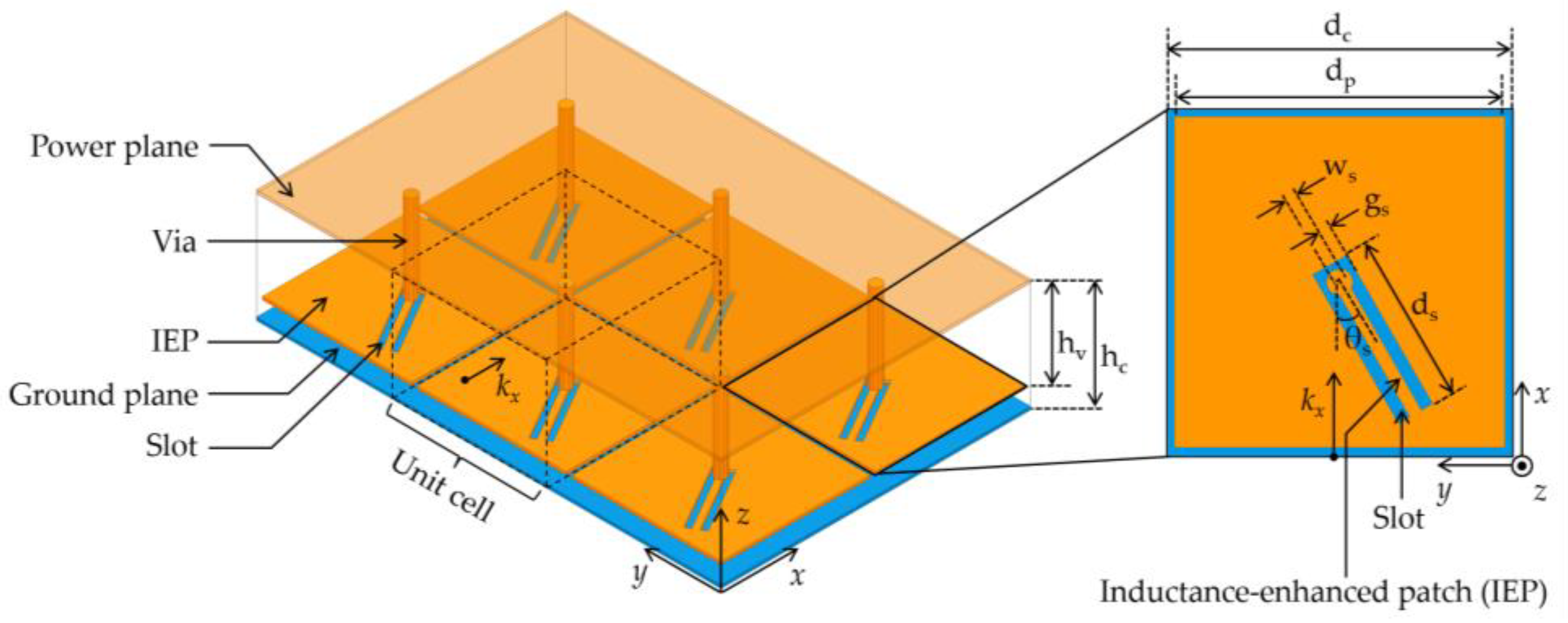
The proposed EBG structure with an inductance-enhanced patch (IEP-EBG) consists of three conducting layers, namely the layers for a power plane, an IEP, and a ground plane, as shown in Figure 1. The power plane is connected to the IEP through a via. In previous EBG structures such as the mushroom-type EBG structure, the via mainly provided inductive characteristics [16]. However, the IEP in the proposed EBG structure further enhances the inductive characteristics.
The IEP is an EBG patch including a U-shape slot. The U-shape slot surrounds the via and generates a narrow bridge connecting the via and a position on the edge of the patch. In practice, an inductive path on the patch is formed. The increase in patch inductance not only results in downsizing of the EBG UC, but also reduces the low cut-off frequency (fL) of the stopband. This feature will be thoroughly analyzed in Section 3.
The proposed IEP technique can be simply realized by etching the patch in a manufacturing process, thus it does not require complicated or additional processes. Moreover, it has the advantages of simple design, cost-effectiveness, and convenience for the analysis of the PPW mode suppression.
The proposed IEP-EBG structure periodically arranges UCs in packages and PCBs. Although Figure 1 shows an IEP-EBG array with 3-by-2 (3 × 2) UCs, the array size is not limited and depends on the board size. The geometric design of the IEP-EBG structure can be explained by determining the physical parameters of the UC. The design parameters associated with the IEP are the ws, ds, gs, and θs of the bridge width, the slot length, the slot width, and the slot rotation angle, respectively. The UC and patch size are depicted as dc and dp, respectively. The distance between the power plane and an IEP is hv, which is equivalent to the via length. hc is the distance between the power plane and the ground plane. Conducting layers (e.g., the power plane) are separated by a dielectric material with relative dielectric permittivity εr.
3. Floquet Analysis
In this section, we performed a dispersion analysis using Floquet’s theory. The dispersion result efficiently showed the stopband characteristics of the IEP-EBG structure. Dispersion diagrams were used to examine the inductance effects of the IEP on a stopband. In addition, using the dispersion results, we demonstrated that the miniaturization of the IEP-EBG structure was superior to that of the mushroom-type EBG structure (i.e., the previous EBG structure without an IEP).
3.1. Analysis of the IEP Effect on Stopband
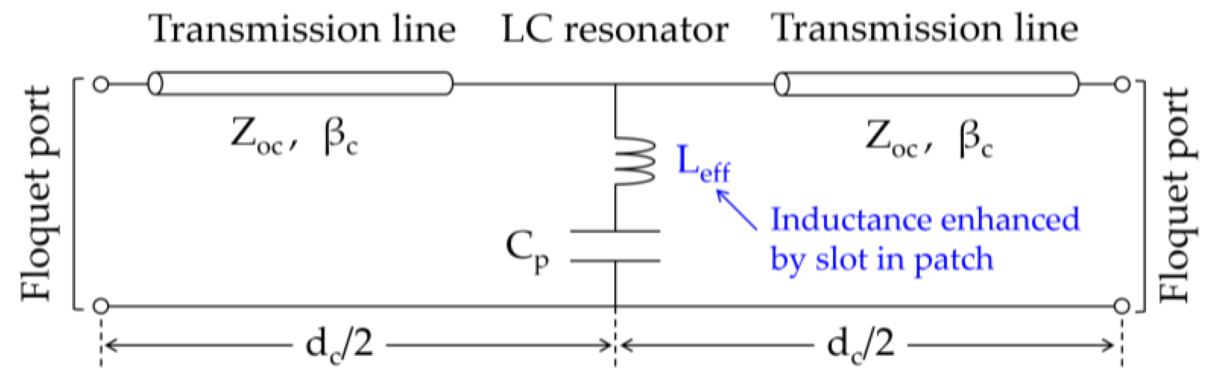
To obtain a dispersion diagram and examine the IEP effects, an equivalent circuit model of the UC of the proposed IEP-EBG structure was derived using transmission lines and a LC resonator, as shown in Figure 2. In the equivalent circuit model, only one-dimensional (1-D) propagation of the SSN is considered to simplify the dispersion analysis. However, it can be extended for a 2-D propagation analysis. The difference in the cut-off frequencies of 1-D and 2-D propagation analysis can be further investigated [17].
As described previously, the IEP technique significantly increases the inductance value of the EBG structure. The inductor enhanced by the IEP technique is represented as Leff in the equivalent circuit model. The transmission line depicts the power and ground planes in the UC, which are vertically separated by the distance hc. Its characteristic impedance Zoc is mainly determined by the UC width dc, dielectric thickness hc, and relative dielectric permittivity εr. The Zoc value can be calculated by the closed-form equation in [12], or numerical field solvers such as HFSS, MWS, and Momentum when physical dimensions are given. The patch and corresponding ground plane forms a capacitor with a capacitance value of Cp. The via and IEP induces an inductance Leff, which is the sum of the via inductance and the patch inductance, which is significantly increased by the IEP. The LC resonator formed by the capacitor and inductor are connected in shunt with transmission lines. The Cp is simply extracted from a rectangular-shape parallel plate capacitor. The via inductance and patch inductance enhanced by the IEP are difficult to extract separately using an analytical equation or numerical solvers. In this paper, the sum of the via and IEP inductances were used as the Leff for the simplicity of analysis.
To obtain the dispersion characteristics, we applied Floquet’s theory to the IEP-EBG structure. Floquet’s theory for periodical structures is based on a UC analysis. It assumes that UCs are arranged periodically and infinitely. Floquet’s theory shows that the voltages and currents at all ports of a UC can be defined, and their relationships are expressed as network parameters. In particular, the use of ABCD parameters results in the simplification of the dispersion analysis for a two-port UC.
For the IEP-EBG structure, the ABCD parameter of the UC is expressed as a product of the ABCD parameters of the transmission lines and the LC resonator circuit as follows:
where
Evaluating the Aeq from the equations above, the dispersion equation is derived in terms of the characteristics of the transmission lines and the resonator circuit. The effective propagation constant βeff is given by
where
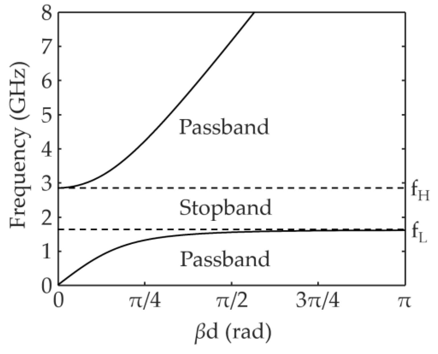
Using Equation (5), we obtained the example of the dispersion diagram of the IEP-EBG structure in Figure 3. The design parameters and corresponding values of the example of the IEP-EBG structure are shown in Table 1. The values were reasonably determined considering the conventional manufacturing processes used for high-speed packages and PCBs.
In the dispersion diagram shown in Figure 3, the passbands and stopbands are shown alternately. In the first stopband, the slow-wave effect is observed and the stopband starts from the low cut-off frequency fL. It is anticipated that the PPW modes are efficiently suppressed in the stopband. As a consequence, the SSN is significantly mitigated over the frequency range from fL to a high cut-off frequency (fH). In this example of the dispersion results, the stopband is obtained in the frequency range from 1.6 GHz to 2.86 GHz.
To thoroughly examine the IEP effects, a closed-form solution of fL was derived by realizing that a real part of βeff·dc was equal to π (i.e., Re{βeff·dc} = π). In addition, we assumed that the value of βeff·dc was too small for the small angle approximation of trigonometric functions in Equation (5) because it was far from the Brillouin zone boundary at the low cut-off frequency. Then, a closed-form expression for fL can be extracted as
where
vp is the phase velocity. c is the speed of light and εeff is the effective relative permittivity of the dielectric material.
Using Equation (7), the IEP effects on fL were characterized by sweeping the Leff values from 0.6 nH to 1.4 nH as shown in Figure 4. The Leff values used herein were chosen considering a conventional design of high-speed packages and PCBs. The fL analysis with Equation (7) was not limited to these values. As can be seen in Figure 4, it was found that the fL value decreased as the Leff value increased. Applying the IEP technique to the EBG structure increased the effective inductance of the EBG UC. As a result, the fL was shifted down in the low frequency range.
The advantage of fL reduction with the IEP technique is the efficient miniaturization of the UC.
When we have a design objective for the fL in high-speed packages and PCBs, the value of the fL can be controlled by changing the dc, Leff, Zoc, and Cp values. To shift the fL down into the low frequency range and satisfy the design target, first, dc can be increased, thus enlarging the UC size. Alternatively, increasing Zoc enables a low fL value. For a large Zoc, the thickness of the packages and PCBs needs to be significantly increased, which is prohibited in most applications of high-speed packages and PCBs. Additionally, increasing Cp reduces the fL value. However, increasing Cp can be accomplished by using a high dielectric constant material, which is a costly and unreliable method.
Instead of these former methods, we increased Leff using the IEP techniques without increasing the UC size, PCB thickness, or cost.
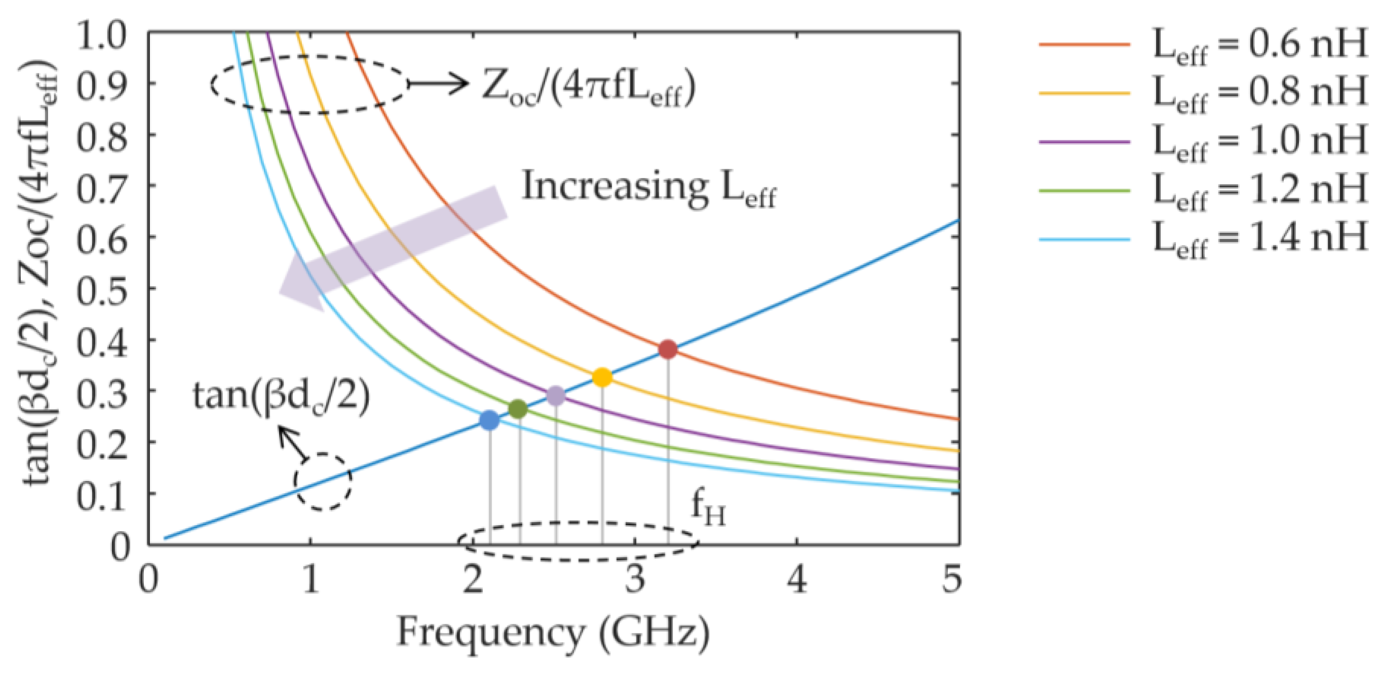
To further examine the IEP effects on the stopband, the high cut-off frequency fH was obtained by applying the condition of βeff = 0 to Equation (5) as follows:
In Equation (9), it was approximated by assuming that the resonance frequency defined by the product Leff·CP was widely separated from the fH. To analyze the IEP effect on the fH, a graphical analysis was adopted by plotting the left- and right-hand sides of Equation (9) as shown in Figure 5. The tangent function of the left-hand side is shown as a blue curve. Five fractional functions of the right-hand side with respect to the various Leff values are represented. The Leff values of 0.6 nH, 0.8 nH, 1.0 nH, 1.2 nH, and 1.4 nH were used. The point where the tangent function curve and the fractional function curve intersect indicates the approximate value of the fH.
As shown in Figure 5, the fH decreased as the Leff increased. Consequently, it is shown that the IEP technique reduced the fL and fH, thus shifting down the stopband in the low frequency range, which resulted in downsizing the UC in the IEP-EBG structure.
3.2. Demonstration of fL Reduction and Miniaturization
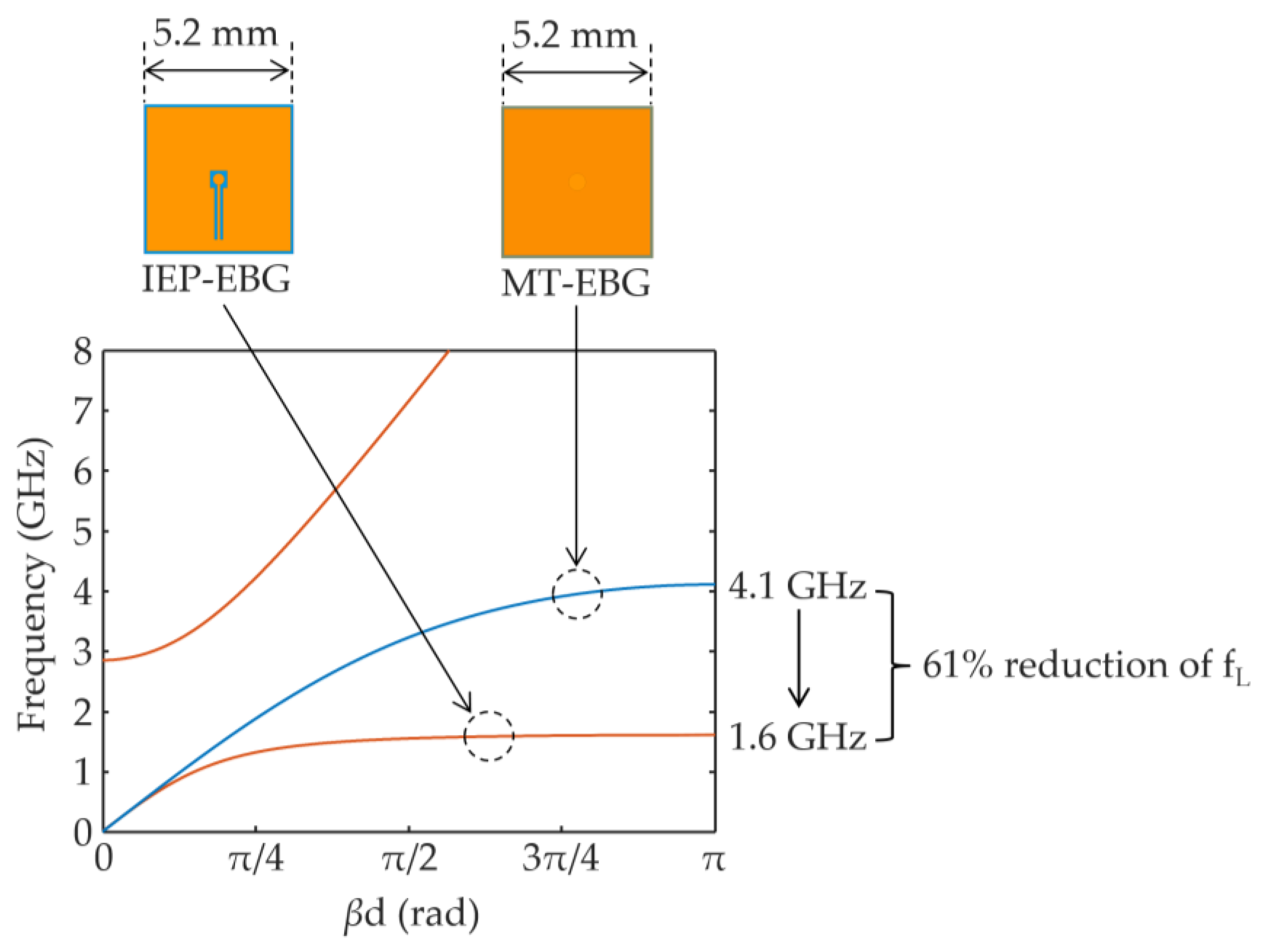
In this section, the fL reduction and miniaturization of the IEP-EBG structure were demonstrated by applying Floquet theory to the example designs. The stopband characteristics of the example designs of the proposed IEP-EBG structures were compared to those of the conventional mushroom-type EBG (MT-EBG) structure. Their dispersion diagrams were derived using Floquet theory based on a full-wave simulation. The ABCD parameters of the proposed IEP-EBG and conventional MT-EBG structures were extracted using finite element method (FEM) simulations performed by HFSS. In this analysis, the FEM simulation technique was employed for a practical design approach based on the geometric design.
The fL reduction was examined for the proposed IEP-EBG and previous MT-EBG structures having the same UC size. The design parameters and corresponding dimensions are summarized in Table 2. The dimensions were selected considering a conventional design guide for high-speed packages and PCBs. The copper and FR-4 were adopted as the metal in the conduction layers and the dielectric material for the example design. The copper thickness and relative permittivity of the dielectric material were assumed to be 18 μm and 4.4, respectively. The dispersion characteristics were extracted as shown in Figure 6. The fL value of the previous MT-EBG structure was 4.1 GHz, while that of the proposed IEP-EBG structure was 1.6 GHz. With the same UC size, the proposed IEP-EBG structure significantly reduced the fL value, up to 61%, when compared to the conventional MT-EBG structure.
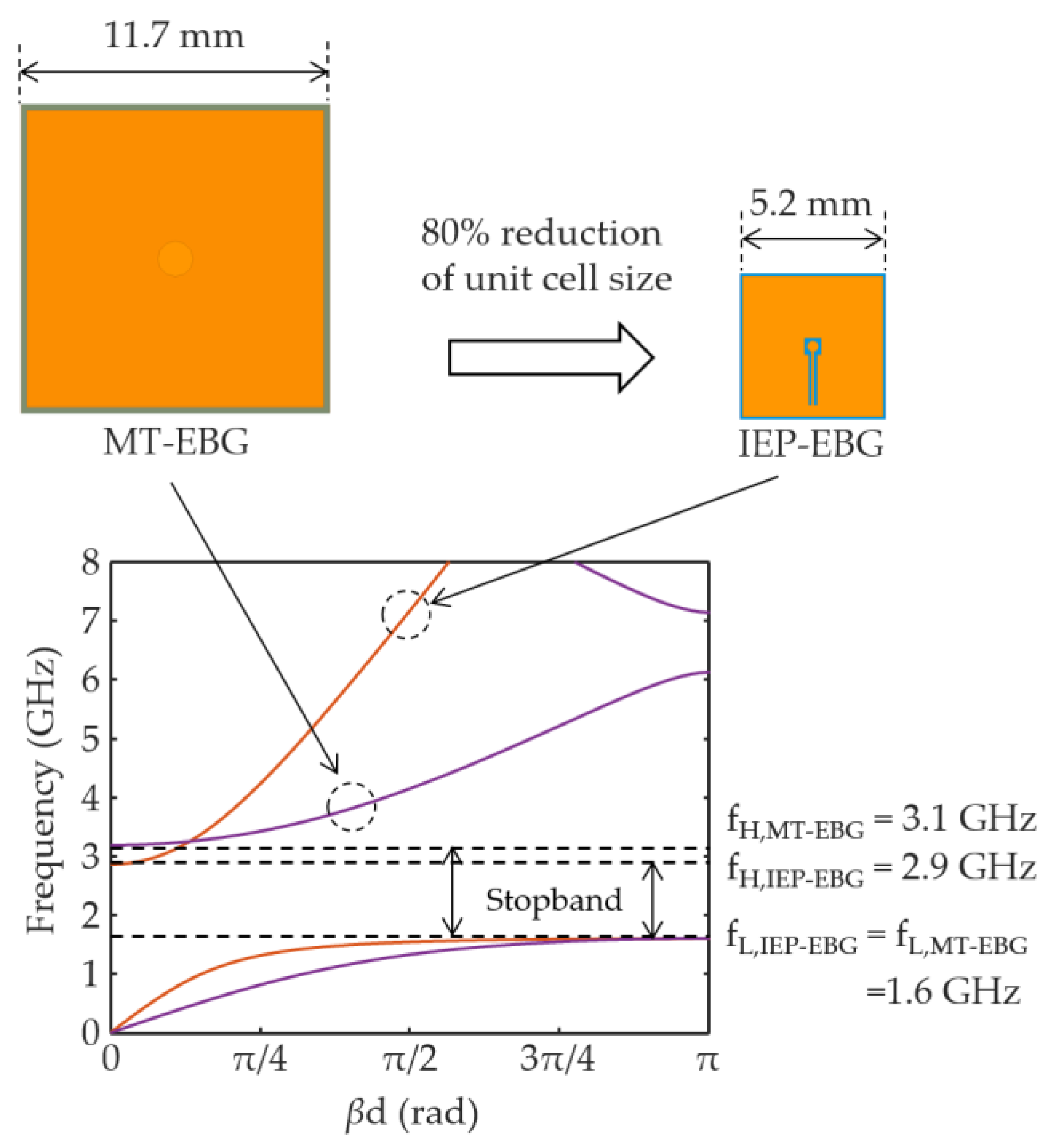
To demonstrate the miniaturization, we compared the dispersion characteristics of the proposed IEP-EBG and previous MT-EBG structures, which had the same fL values of 1.6 GHz, as shown in Figure 7. The dimensions of the IEP-EBG structure were the same as the example structure shown in the fL reduction analysis. The MT-EBG structure was enlarged from 5.2 mm to 11.7 mm to have the same fL as the IEP-EBG structure.
As shown in Figure 7, the IEP structure achieved a significant reduction in UC size when compared to the MT-EBG structure, while the stopband of the IEP-EBG structure was not significantly reduced. An 80% size reduction was accomplished using the IEP technique without stopband deterioration, additional materials, or cost increase. In the analysis, the distinguished characteristics of the fL reduction and miniaturization of the IEP-EBG structure were proven for the specific design. However, it should be noted that the design is not limited to just this specific case.
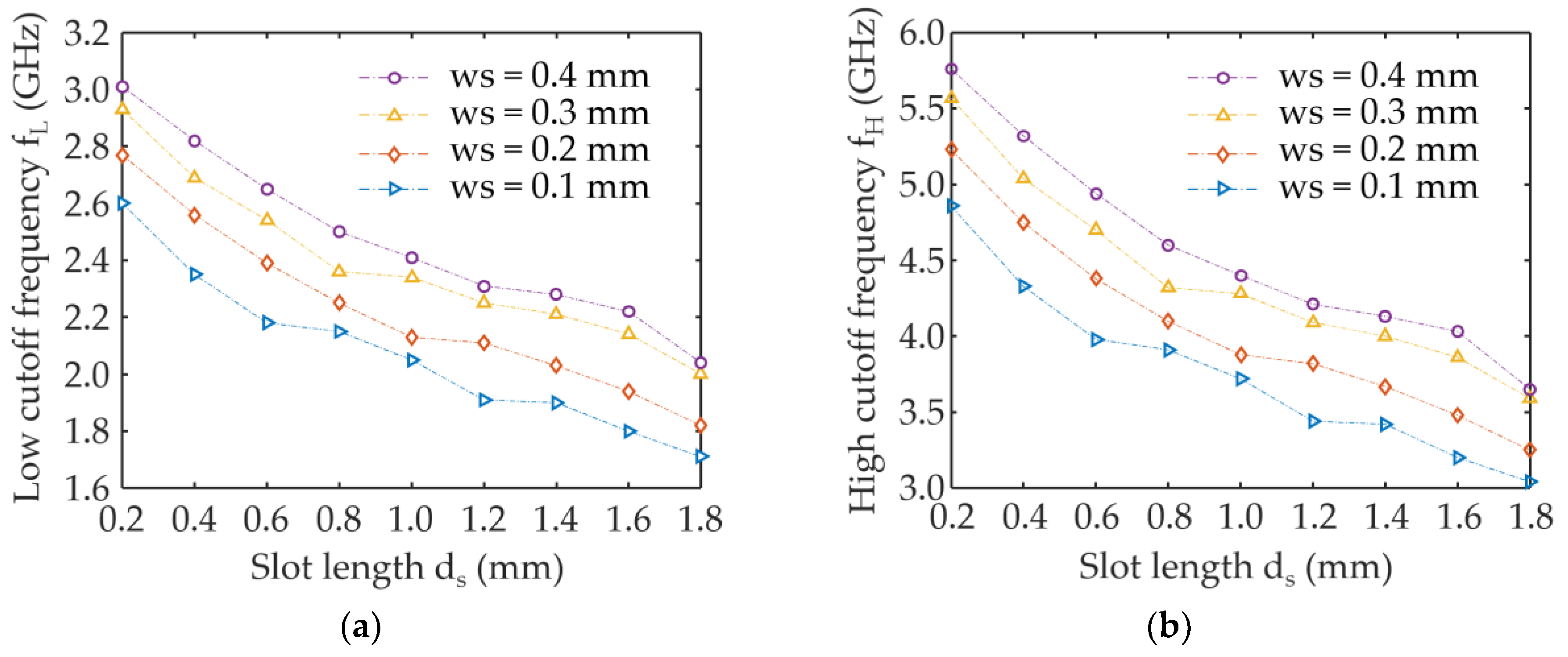
To further investigate the effects of design parameters such as the slot length ds and the slot rotation angle θs, the stopband characteristics were obtained using Floquet analysis for various values of design parameters. Figure 8 depicts the effects of slot length on the fL and fH with respect to various slot length values, varying from 0.2 mm to 1.8 mm. As shown in Figure 8, the fL and fH were approximately inversely proportional to the slot length ds. This can be explained by the ds increase, resulting in the large effective inductance Leff of the UC and lowering of the stopband.
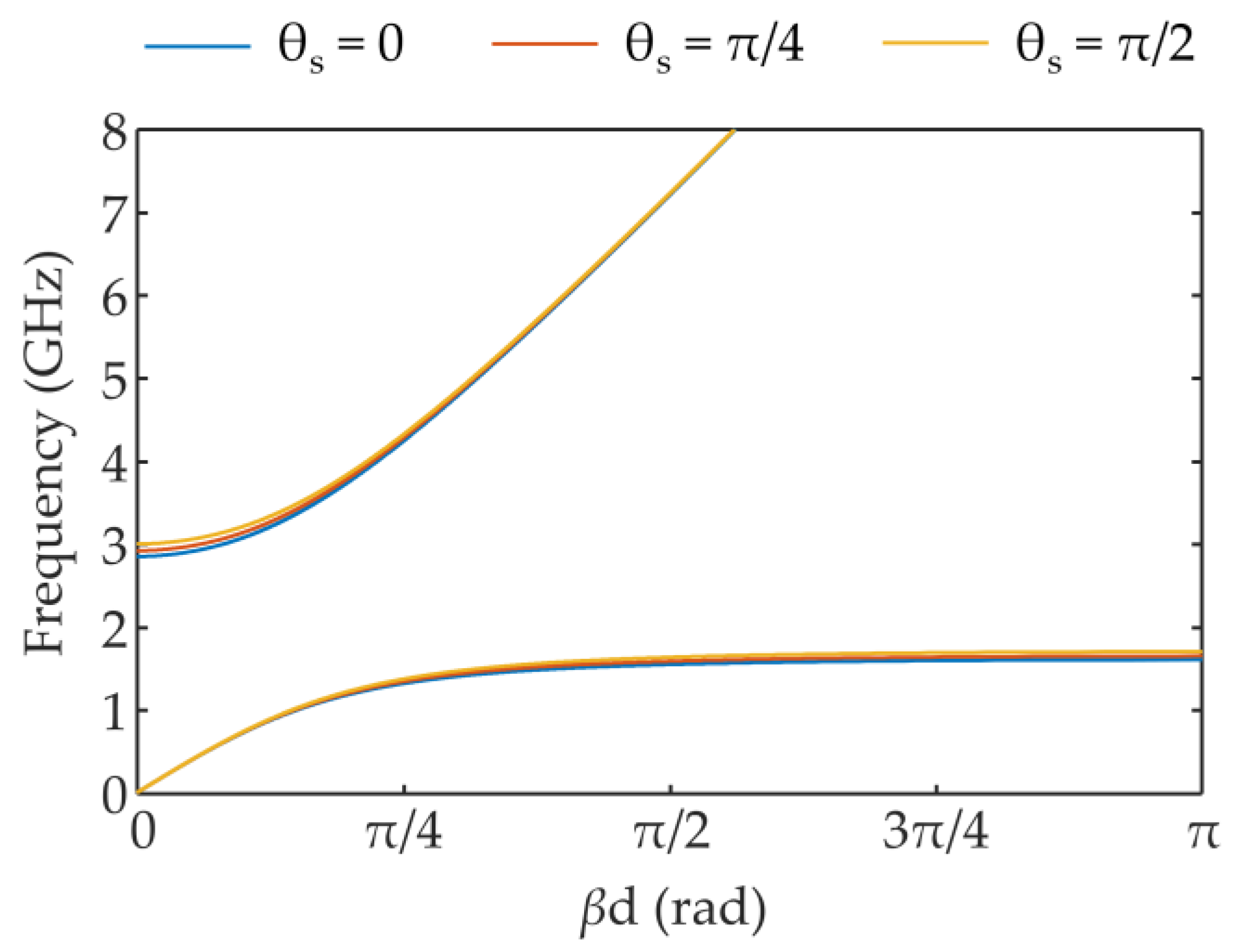
The dispersion characteristics were compared for three cases of the slot rotation angle 0, π/4, and π/2 radians in Figure 9. The Floquet analysis was performed for those cases. As seen in the results, fL and fH were not significantly different for the various slot rotation angles. Even though only a few cases were examined, it can be reasonably concluded that the Leff was not significantly affected by the slot rotation angle. Moreover, the stopband of the IEP-EBG structure was mainly influenced by the slot length. The design of the proposed IEP-EBG structure was simply achieved by adjusting the slot length.
4. Experimental Results
To experimentally verify the IEP-EBG structure, test vehicles (TVs) were fabricated using a commercial PCB manufacturing process with a plated through hole (PTH) via. Copper and FR-4 were used as the conductor and dielectric material in the PCB process. The copper thickness was 18 μm. The relative dielectric permittivity and loss tangent were 4.4 and 0.02, respectively. The PTH via radius was 0.4 mm. Three TVs were fabricated, namely the proposed IEP-EBG structure, the conventional MT-EBG structure, and a PPW as a reference. The physical dimensions of the UCs of the IEP- and MT-EBG structures were the same as the example structure in Table 2. The TVs for the IEP- and MT-EBG structures contained a 7-by-7 array of UCs.
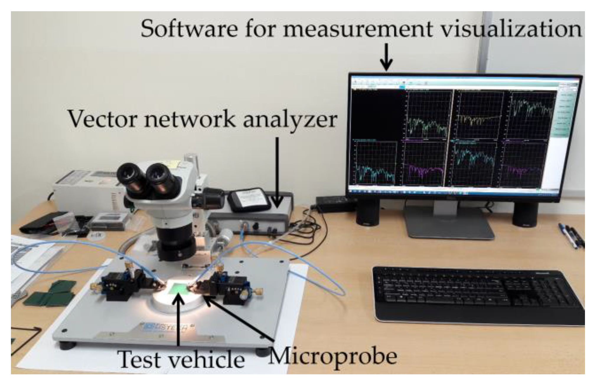
To measure the S21 parameter, a vector network analyzer (model: Anritsu MS46122A) was used, as shown in Figure 10. A microprobe (GGB 40A-GSG-500-DP) with 500-μm pitch was used to minimize parasitic components induced by the additional structure used for the measurement. The probe pads were located at (6 mm, 18.5 mm) and (32 mm, 18.5 mm) with the origin located at the lower left corner of the TVs. The overall board size of the three TVs was 37 mm × 37 mm.
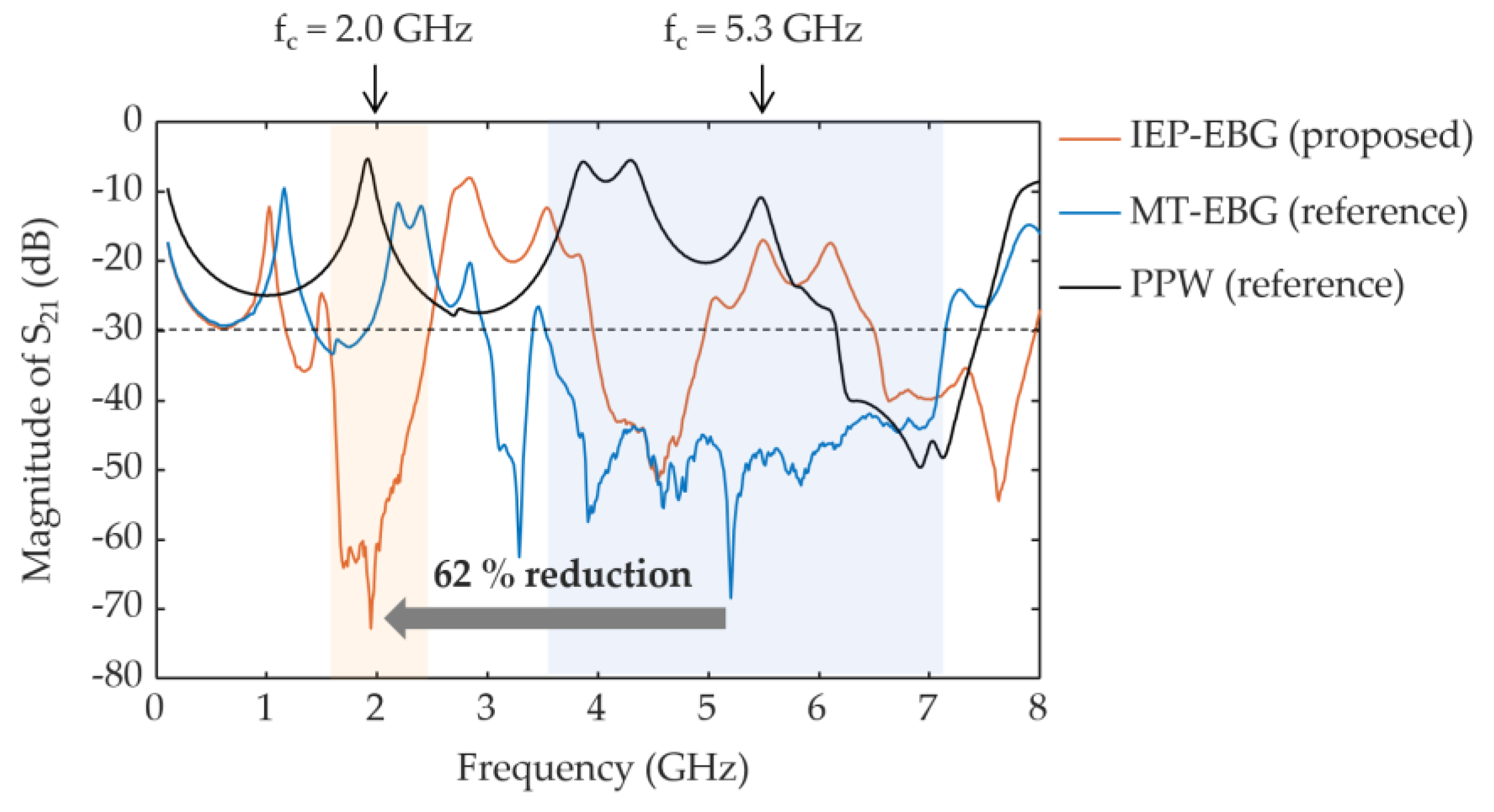
The measured S21 parameters of the proposed IEP-EBG structure, the previous MT-EBG structure, and the PPW are compared in Figure 11. As seen in the results, numerous resonance peaks induced by PPW modes can be observed in the TV of the PPW, represented as a black curve. In contrast, the IEP- and MT-EBG structures formed the stopband, suppressing the PPW modes. The stopband of the MT-EBG structure with a −30 dB suppression level was formed in the frequency range of 3.52 GHz to 7.14 GHz, while that of the IEP-EBG structure was observed in the frequency range 1.55 GHz to 2.48 GHz. The center frequencies fC of the MT- and IEP-EBG structures were approximately 5.3 GHz and 2.0 GHz, respectively.
With the same UC size, the IEP-EBG structure achieved a substantial reduction in fC when compared to the MT-EBG structure by effectively shifting down the stopband in the low frequency range. The distinguishing feature of the IEP-EBG structure was the 62% reduction in the fL without the use of additional materials or layers. The performance of the MT- and IEP-EBG structures could be compared using the FSV technique [18,19,20].
Thus, it resulted in a cost-effective solution. As previously analyzed, the UC of the MT-EBG structure would have to be enlarged up to 11.7 mm to achieve the same stopband as the IEP-EBG structure. Consequently, it was experimentally verified that the IEP-EBG structure achieved superior fL reduction, which resulted in the significant miniaturization of the EBG structure.
5. Conclusions
An inductance-enhanced patch (IEP) technique was presented that efficiently miniaturized the EBG structure while suppressing the PPW modes in high-speed packages and PCBs. The IEP effects on the stopband of the EBG structure were thoroughly examined using a dispersion diagram obtained from Floquet theory. The effective inductance of the IEP-EBG structure significantly increased, so that the stopband including the low cut-off frequency was substantially shifted down into the low frequency range without increasing the UC size of the EBG structure. It was experimentally verified that the IEP-EBG structure achieved a 62% reduction in the center frequency of the stopband when compared to a conventional MT-EBG structure. Moreover, the miniaturized IEP-EBG structure contained no reference discontinuity, so it had good signal integrity characteristics. The IEP-EBG structure is suitable for applications such as mobile devices which require a small form factor with good noise suppression characteristics
Acknowledgments
This work was supported by the National Research Foundation of Korea (NRF) grant funded by the Korean government (Ministry of Science, ICT & Future Planning) (NRF-2016R1C1B1007123).
Conflicts of Interest
The author declares no conflict of interest.
References
- Li, E.; Wei, X.; Angellaris, A.; Liu, E.; Zhang, Y.; D’Amore, M.; Kim, J.; Sudo, T. Progress Review of Electromagnetic Compatibility Analysis Technologies for Packages, Printed Circuit Boards, and Novel Interconnects. IEEE Trans. Electromagn. Compat. 2010, 52, 248–265. [Google Scholar]
- Swaminathan, M.; Chung, D.; Grivet-Talocia, S.; Bharath, K.; Laddha, V.; Xie, J. Designing and Modeling for Power Integrity. IEEE Trans. Electromagn. Compat. 2010, 52, 288–310. [Google Scholar] [CrossRef]
- Muthana, P.; Srinivasan, K.; Engin, A.; Swaminathan, M.; Tummala, R.; Sundaram, V.; Wiedenman, B.; Amey, D.; Dietz, K.; Banerji, S.; et al. Improvements in Noise Suppression for I/O Circuits Using Embedded Planar Capacitors. IEEE Trans. Adv. Packag. 2008, 31, 234–245. [Google Scholar] [CrossRef]
- Choi, J.Y.; Swaminathan, M. Decoupling Capacitor Placement in Power Delivery Networks Using MFEM. IEEE Trans. Compon. Packag. Manuf. Technol. 2011, 1, 1651–1661. [Google Scholar] [CrossRef]
- Li, M.; Ma, K.; Hockanson, D.M.; Drewniak, J.L.; Hubing, T.H.; Van Doren, T.P. Numerical and experimental corroboration of an FDTD thin-slot model for slots near corners of shielding enclosures. IEEE Trans. Electromagn. Compat. 1997, 39, 225–232. [Google Scholar]
- Abhari, R.; Eleftheriades, G.V. Metallo-dielectric electromagnetic bandgap structures for suppression and isolation of the parallel-plate noise in high-speed circuits. IEEE Trans. Microw. Theory Tech. 2003, 51, 1629–1639. [Google Scholar] [CrossRef]
- Wu, T.; Wang, C.; Lin, Y.; Wang, T.; Chang, G. A novel power plane with super-wideband elimination of ground bounce noise on high speed circuits. IEEE Microw. Wirel. Compon. Lett. 2005, 15, 174–176. [Google Scholar]
- Kim, K.H.; Schutt-Aine, J.E. Design of EBG Power Distribution Networks With VHF-Band Cutoff Frequency and Small Unit Cell Size for Mixed-Signal Systems. IEEE Microw. Wirel. Compon. Lett. 2007, 17, 489–491. [Google Scholar] [CrossRef]
- Choi, J.; Govind, V.; Swaminathan, M.; Bharath, K. Noise Isolation in Mixed-Signal Systems Using Alternating Impedance Electromagnetic Bandgap (AI-EBG) Structure-Based Power Distribution Network (PDN). IEEE Trans. Adv. Packag. 2010, 33, 2–12. [Google Scholar] [CrossRef]
- Shahparnia, S.; Ramahi, O.M. Simultaneous switching noise mitigation in PCB using cascaded high-impedance surfaces. Electron. Lett. 2004, 40, 98–100. [Google Scholar] [CrossRef]
- Zhang, M.S.; Li, Y.S.; Jia, C.; Li, L.P. A Power Plane with Wideband SSN Suppression Using a Multi-Via Electromagnetic Bandgap Structure. IEEE Microw. Wirel. Compon. Lett. 2007, 17, 307–309. [Google Scholar] [CrossRef]
- Kim, M.; Koo, K.; Hwang, C.; Shim, Y.; Kim, J.; Kim, J. A Compact and Wideband Electromagnetic Bandgap Structure Using a Defected Ground Structure for Power/Ground Noise Suppression in Multilayer Packages and PCBs. IEEE Trans. Electromagn. Compat. 2012, 54, 689–695. [Google Scholar]
- Kim, M.; Kam, D.G. A Wideband and Compact EBG Structure with a Circular Defected Ground Structure. IEEE Trans. Compon. Packag. Manuf. Technol. 2014, 4, 496–503. [Google Scholar] [CrossRef]
- Lee, J.; Kim, H.; Kim, J. High dielectric constant thin film EBG power/ground network for broad-band suppression of SSN and radiated emissions. IEEE Microw. Wirel. Compon. Lett. 2005, 15, 505–507. [Google Scholar]
- Kim, M.; Koo, K.; Shim, Y.; Hwang, C.; Pak, J.; Ahn, S.; Kim, J. Vertical Stepped Impedance EBG (VSI-EBG) Structure for Wideband Suppression of Simultaneous Switching Noise in Multilayer PCBs. IEEE Trans. Electromagn. Compat. 2013, 55, 307–314. [Google Scholar] [CrossRef]
- Rogers, S.D. Electromagnetic-Bandgap Layers for Broad-Band Suppression of TEM Modes in Power Planes. IEEE Trans. Microw. Theory Tech. 2005, 53, 2495–2505. [Google Scholar] [CrossRef]
- Toyota, Y.; Engin, A.E.; Kim, T.H.; Swaminathan, M. Stopband Analysis Using Dispersion Diagram for Two-Dimensional Electromagnetic Bandgap Structures in Printed Circuit Boards. IEEE Microw. Wirel. Compon. Lett. 2006, 16, 645–647. [Google Scholar] [CrossRef]
- IEEE Standard P1597. Standard for Validation of Computational Electromagnetics Computer Modeling and Simulation—Part 1, 2; IEEE: Piscataway, NJ, USA, 2008. [Google Scholar]
- Duffy, A.; Orlandi, A.; Zhang, G. Review of the Feature Selective Validation Method (FSV). Part I: Theory. IEEE Trans. Electromagn. Compat. 2018, 6, 814–821. [Google Scholar] [CrossRef]
- Orlandi, A.; Duffy, A.P.; Zhang, G. Review of the Feature Selective Validation Method. Part II: Performance Analysis and Research Fronts. IEEE Trans. Electromagn. Compat. 2018, 6, 1029–1035. [Google Scholar] [CrossRef]
Figure 1.
A proposed EBG structure using an inductance-enhanced patch (IEP-EBG) within the design parameters of a unit cell.
Figure 1.
A proposed EBG structure using an inductance-enhanced patch (IEP-EBG) within the design parameters of a unit cell.

Figure 2.
An equivalent circuit model of the UC of the proposed structure using an inductance-enhanced patch (IEP-EBG) for Floquet analysis.
Figure 2.
An equivalent circuit model of the UC of the proposed structure using an inductance-enhanced patch (IEP-EBG) for Floquet analysis.

Figure 3.
Dispersion diagram of the IEP-EBG structure showing the stopband characteristics.

Figure 4.
Analysis of the IEP effects on the low cut-off frequency fL with various Leff values.
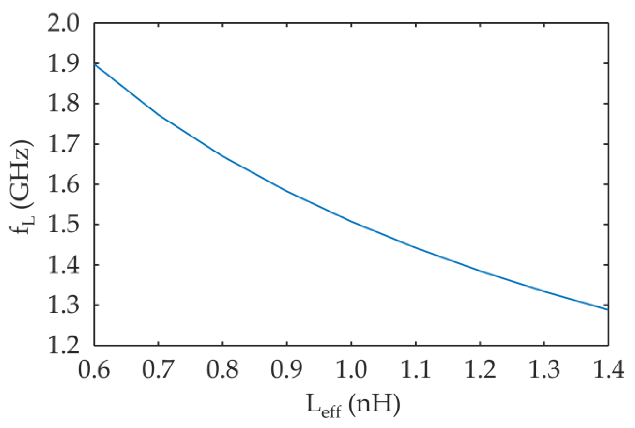
Figure 5.
IEP effects on the high cut-off frequency fH with various Leff values.

Figure 6.
Dispersion analysis of the fL reduction of the IEP-EBG structure.

Figure 7.
Miniaturization analysis of the UC of the IEP-EBG structure using a dispersion diagram.

Figure 8.
Slot length effects on (a) the low cut-off frequency fL and (b) high cut-off frequency fH.
Figure 8.
Slot length effects on (a) the low cut-off frequency fL and (b) high cut-off frequency fH.

Figure 9.
Dispersion diagram for the slot rotation angle effects.

Figure 10.
Measurement setup of S-parameters for the verification of the IEP-EBG structure.

Figure 11.
S21 measurements of the IEP- and MT-EBG structures, and the PPW.


Table 1.
Design parameters and corresponding values for the dispersion analysis.
| Parameters | dc | Zoc | Cp | εr | Leff |
|---|---|---|---|---|---|
| Values | 5.2 mm | 9.2 Ω | 10.3 pF | 4.4 | 0.9 nH |
Table 2.
Design parameters and corresponding values of the dispersion analysis.
| Parameters | dc | dp | ws | ds | gs | θs | hv | hc |
|---|---|---|---|---|---|---|---|---|
| Values | 5.2 mm | 5 mm | 0.1 mm | 1.8 mm | 0.1 mm | 0 rad | 0.2 mm | 0.3 mm |
© 2018 by the author. Licensee MDPI, Basel, Switzerland. This article is an open access article distributed under the terms and conditions of the Creative Commons Attribution (CC BY) license (http://creativecommons.org/licenses/by/4.0/).
Share and Cite
MDPI and ACS Style
Kim, M. A Miniaturized Electromagnetic Bandgap Structure Using an Inductance-Enhanced Patch for Suppression of Parallel Plate Modes in Packages and PCBs. Electronics 2018, 7, 76. https://doi.org/10.3390/electronics7050076
AMA Style
Kim M. A Miniaturized Electromagnetic Bandgap Structure Using an Inductance-Enhanced Patch for Suppression of Parallel Plate Modes in Packages and PCBs. Electronics. 2018; 7(5):76. https://doi.org/10.3390/electronics7050076
Chicago/Turabian StyleKim, Myunghoi. 2018. "A Miniaturized Electromagnetic Bandgap Structure Using an Inductance-Enhanced Patch for Suppression of Parallel Plate Modes in Packages and PCBs" Electronics 7, no. 5: 76. https://doi.org/10.3390/electronics7050076
Note that from the first issue of 2016, this journal uses article numbers instead of page numbers. See further details here.