
Comparison of MOCVD and MBE Regrowth for CAVET Fabrication

 ,
,
Abstract
1. Introduction
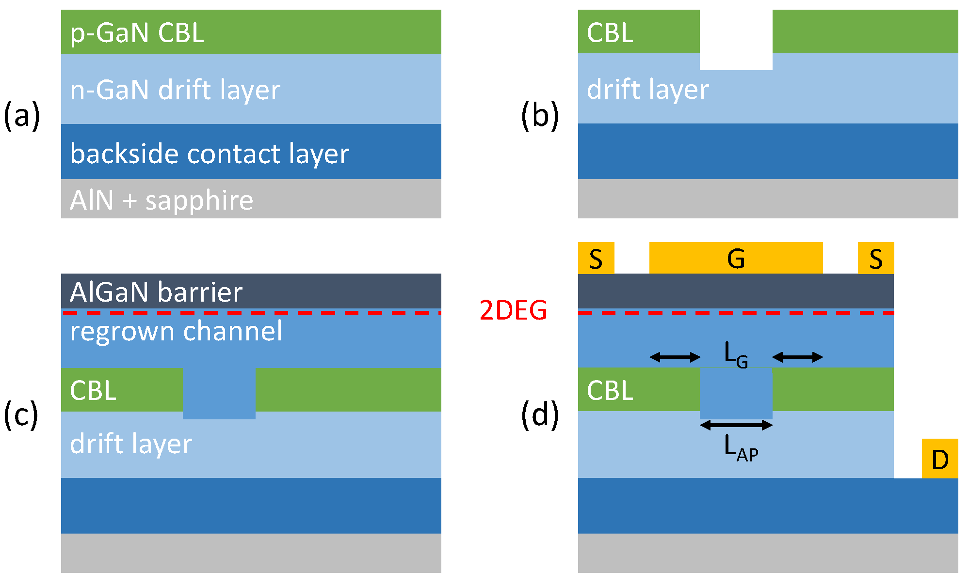
2. Experiment
3. Results and Discussion
3.1. Structural Characterization
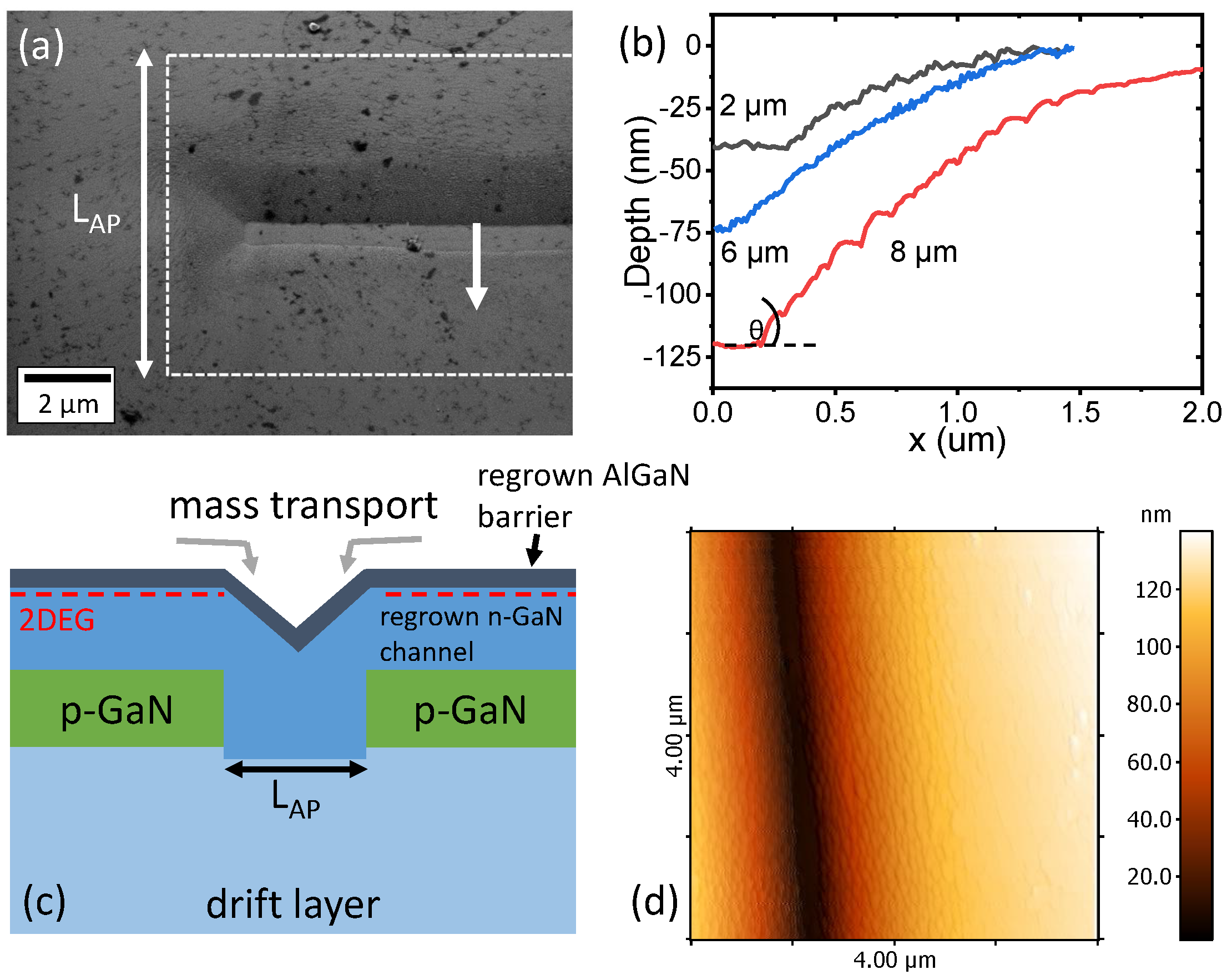
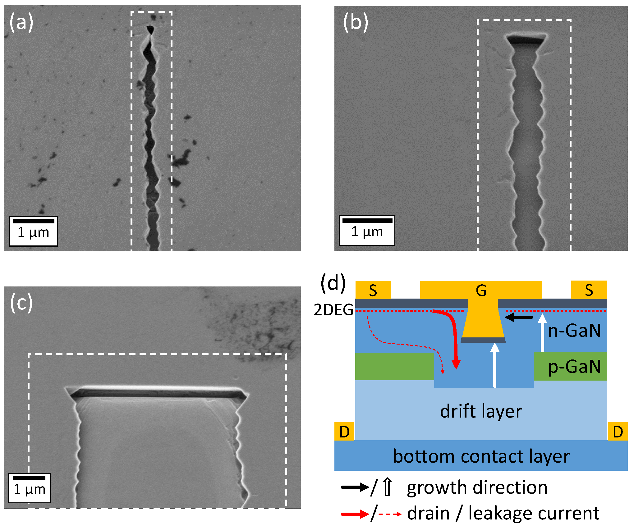
3.1.1. MOCVD Regrowth
3.1.2. MBE Regrowth
3.2. Electrical Characterization
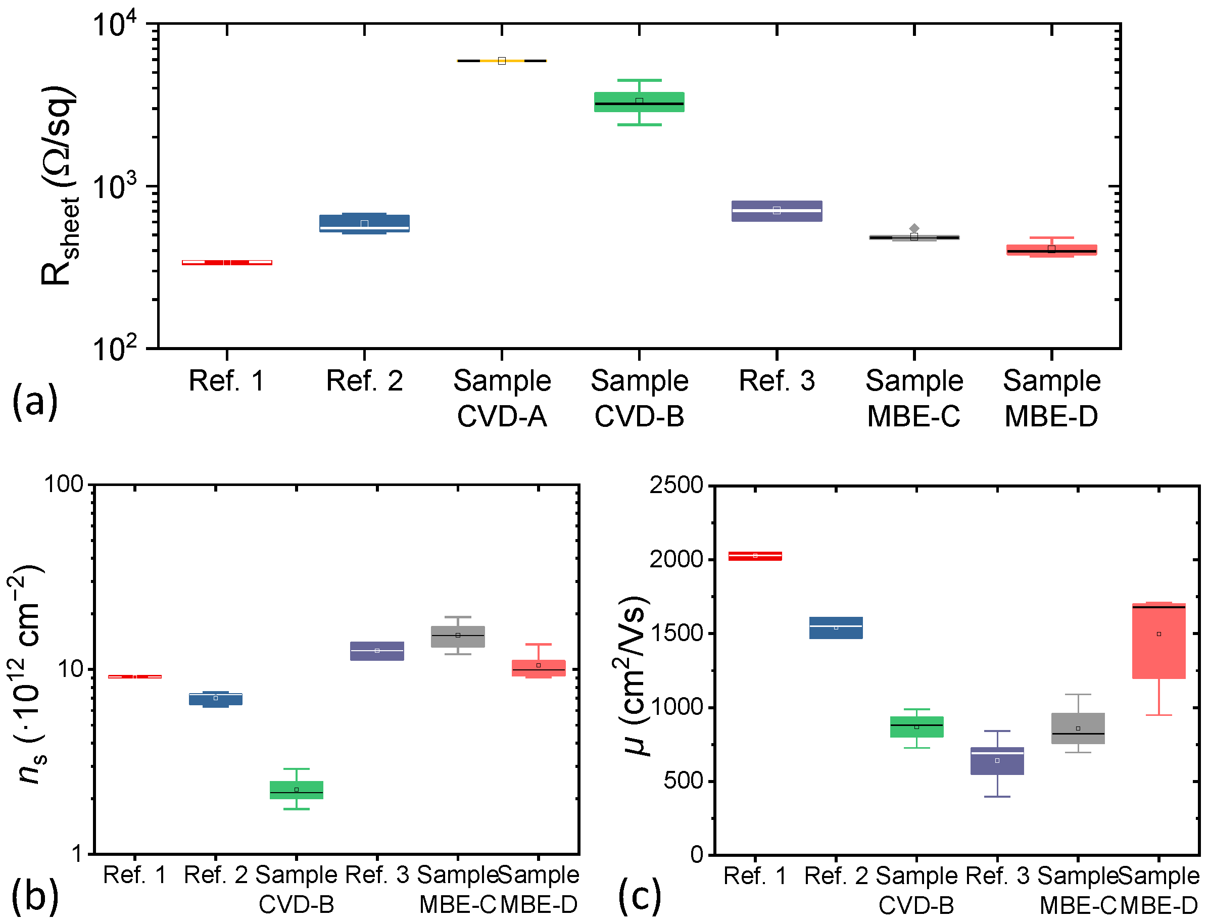
3.2.1. Planar 2DEG Properties
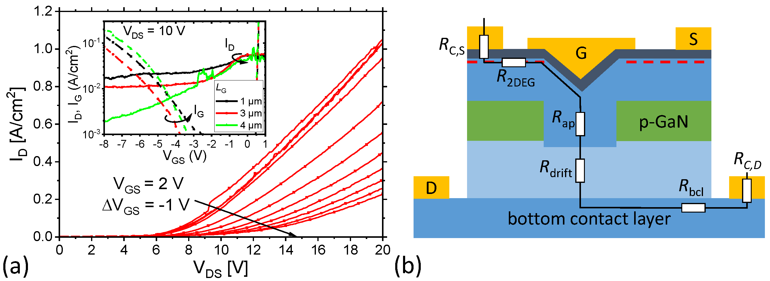
3.2.2. MOCVD-Regrown CAVET (CVD-A)
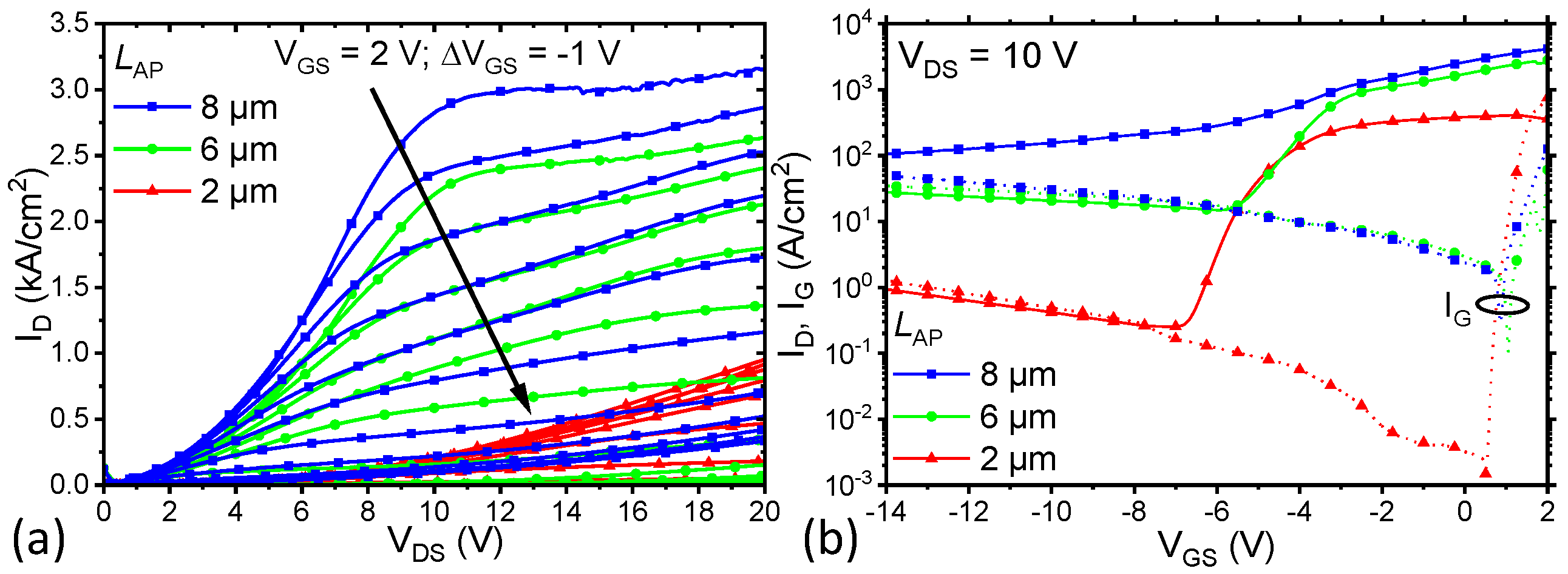
3.2.3. MBE-Regrown CAVET (MBE-D)
4. Summary and Conclusions
Author Contributions
Funding
Conflicts of Interest
References
- Jones, E.A.; Wang, F.F.; Costinett, D. Review of Commercial GaN Power Devices and GaN-Based Converter Design Challenges. IEEE J. Emerg. Sel. Top. Power Electron. 2016, 4, 707–719. [Google Scholar] [CrossRef] [Scilit]
- Chowdhury, S. GaN-on-GaN power device design and fabrication. In Wide Bandgap Semiconductor Power Devices; Elsevier: Amsterdam, The Netherlands, 2019; pp. 209–248. [Google Scholar]
- Chowdhury, S.; Mishra, U.K. Lateral and Vertical Transistors Using the AlGaN/GaN Heterostructure. IEEE Trans. Electron Devices 2013, 60, 3060–3066. [Google Scholar] [CrossRef] [Scilit]
- Li, W.; Chowdhury, S. Design and fabrication of a 1.2 kV GaN-based MOS vertical transistor for single chip normally off operation. Phys. Status Solidi 2016, 213, 2714–2720. [Google Scholar] [CrossRef] [Scilit]
- Gupta, C.; Lund, C.; Chan, S.H.; Agarwal, A.; Liu, J.; Enatsu, Y.; Keller, S.; Mishra, U.K. In Situ Oxide, GaN Interlayer-Based Vertical Trench MOSFET (OG-FET) on Bulk GaN substrates. IEEE Electron Device Lett. 2017, 38, 353–355. [Google Scholar] [CrossRef] [Scilit]
- Sun, M.; Zhang, Y.; Gao, X.; Palacios, T. High-Performance GaN Vertical Fin Power Transistors on Bulk GaN Substrates. IEEE Electron Device Lett. 2017, 38, 509–512. [Google Scholar] [CrossRef] [Scilit]
- Zhang, Y.; Sun, M.; Piedra, D.; Hu, J.; Liu, Z.; Lin, Y.; Gao, X.; Shepard, K.; Palacios, T. 1200 V GaN vertical fin power field-effect transistors. In Proceedings of the 2017 IEEE International Electron Devices Meeting (IEDM), San Francisco, CA, USA, 2–6 December 2017. [Google Scholar]
- Kizilyalli, I.; Aktas, O. Characterization of vertical GaN p-n diodes and junction field-effect transistors on bulk GaN down to cryogenic temperatures. Semicond. Sci. Technol. 2015, 30, 124001. [Google Scholar] [CrossRef] [Scilit]
- Ji, D.; Chowdhury, S. Design of 1.2 kV Power Switches With Low RON Using GaN-Based Vertical JFET. IEEE Trans. Electron Devices 2015, 62, 2571–2578. [Google Scholar]
- Kotzea, S.; Debald, A.; Heuken, M.; Kalisch, H.; Vescan, A. Demonstration of a GaN-Based Vertical-Channel JFET Fabricated by Selective-Area Regrowth. IEEE Trans. Electron Devices 2018, 65, 5329–5336. [Google Scholar] [CrossRef] [Scilit]
- Ben-Yaacov, I. AlGaN/GaN Current Aperture Vertical Electron Transistors. Ph.D. Thesis, University of California, Santa Barbara, CA, USA, 2004. [Google Scholar]
- Ben-Yaacov, I.; Seck, Y.K.; Mishra, U.K.; DenBaars, S.P. AlGaN/GaN current aperture vertical electron transistors with regrown channels. J. Appl. Phys. 2004, 95, 2073–2078. [Google Scholar] [CrossRef] [Scilit]
- Chowdhury, S. Aluminum Gallium Nitride/Gallium Nitride CAVETs for High Power Switching Application. Ph.D. Thesis, University of California, Santa Barbara, CA, USA, 2010. [Google Scholar]
- Chowdhury, S.; Wong, M.H.; Swenson, B.L.; Mishra, U.K. CAVET on Bulk GaN Substrates Achieved With MBE-Regrown AlGaN/GaN Layers to Suppress Dispersion. IEEE Electron. Device Lett. 2012, 33, 41–43. [Google Scholar] [CrossRef] [Scilit]
- Mandal, S.; Agarwal, A.; Ahmadi, E.; Bhat, K.M.; Ji, D.; Laurent, M.A.; Keller, S.; Chowdhury, S. Dispersion Free 450-V p GaN-Gated CAVETs With Mg-ion Implanted Blocking Layer. IEEE Electron. Device Lett. 2017, 38, 933–936. [Google Scholar] [CrossRef] [Scilit]
- Ji, D.; Laurent, M.A.; Agarwal, A.; Li, W.; Mandal, S.; Keller, S.; Chowdhury, S. Normally OFF Trench CAVET With Active Mg-Doped GaN as Current Blocking Layer. IEEE Trans. Electron. Devices 2017, 64, 805–808. [Google Scholar] [CrossRef] [Scilit]
- Ji, D.; Agarwal, A.; Li, W.; Keller, S.; Chowdhury, S. Demonstration of GaN Current Aperture Vertical Electron Transistors With Aperture Region Formed by Ion Implantation. IEEE Trans. Electron Devices 2018, 65, 483–487. [Google Scholar] [CrossRef] [Scilit]
- Gao, Y.; Ben-Yaacov, I.; Mishra, U.K.; Hu, E.L. Optimization of AlGaN/GaN current aperture vertical electron transistor (CAVET) fabricated by photoelectrochemical wet etching. J. Appl. Phys. 2004, 96, 6925–6927. [Google Scholar] [CrossRef] [Scilit]
- Debald, A.; Kotzea, S.; Heuken, M.; Kalisch, H.; Vescan, A. Growth and Characterization of Vertical and Lateral p-n Junctions Formed by Selective-Area p-GaN MOVPE on Patterned Templates. Phys. Status Solidi 2018, 216, 1800677. [Google Scholar] [CrossRef] [Scilit]
- Sze, S.M.; Ng, K.K. Physics of Semiconductor Devices; John Wiley & Sons: Hoboken, NJ, USA, 2006. [Google Scholar]
- Witte, W. Building Blocks of Vertical GaN-Based Devices. Ph.D. Thesis, RWTH Aachen University, Aachen, Germany, 2016. [Google Scholar]
- Hahn, H.; Lükens, G.; Ketteniss, N.; Kalisch, H.; Vescan, A. Recessed-Gate Enhancement-Mode AlGaN/GaN Heterostructure Field-Effect Transistors on Si with Record DC Performance. Appl. Phys. Express 2011, 4, 114102. [Google Scholar] [CrossRef] [Scilit]
- Reuters, B.; Hahn, H.; Behmenburg, H.; Heuken, M.; Kalisch, H.; Vescan, A. Insulating behavior of interfaces in regrown Al0.23Ga0.77N/GaN double heterostructures on Al0.07Ga0.93N back-barrier templates. Phys. Status Solidi 2013, 10, 799–802. [Google Scholar] [CrossRef] [Scilit]
- Xing, H.; Green, D.S.; Yu, H.; Mates, T.; Kozodoy, P.; Keller, S.; DenBaars, S.P.; Mishra, U.K. Memory Effect and Redistribution of Mg into Sequentially Regrown GaN Layer by Metalorganic Chemical Vapor Deposition. Jpn. J. Appl. Phys. 2003, 42, 50–53. [Google Scholar] [CrossRef] [Scilit]
- Chowdhury, S.; Swenson, B.L.; Lu, J.; Mishra, U.K. Use of Sub-nanometer Thick AlN to Arrest Diffusion of Ion-Implanted Mg into Regrown AlGaN/GaN Layers. Jpn. J. Appl. Phys. 2011, 50, 101002. [Google Scholar] [CrossRef] [Scilit]
- Tomita, K.; Itoh, K.; Ishiguro, O.; Kachi, T.; Sawaki, N. Reduction of Mg segregation in a metalorganic vapor phase epitaxial grown GaN layer by a low-temperature AlN interlayer. J. Appl. Phys. 2008, 104, 014906. [Google Scholar] [CrossRef] [Scilit]
- Heikman, S.; Keller, S.; Moran, B.; Coffie, R.; DenBaars, S.; Mishra, U. Mass Transport Regrowth of GaN for Ohmic Contacts to AlGaN/GaN. Phys. Status Solidi 2001, 188, 355–358. [Google Scholar] [CrossRef]
- Zanato, D.; Gokden, S.; Balkan, N.; Ridley, B.K.; Schaff, W.J. The effect of interface-roughness and dislocation scattering on low temperature mobility of 2D electron gas in GaN/AlGaN. Semicond. Sci. Technol. 2004, 19, 427–432. [Google Scholar] [CrossRef] [Scilit]
- Lisesivdin, S.B.; Acar, S.; Kasap, M.; Ozcelik, S.; Gokden, S.; Ozbay, E. Scattering analysis of 2DEG carrier extracted by QMSA in undoped Al0.25Ga0.75N/GaN heterostructures. Semicond. Sci. Technol. 2007, 22, 543–548. [Google Scholar] [CrossRef] [Scilit]



| Sample | Technique | Remark | |
|---|---|---|---|
| CVD-A | MOCVD | 1050 °C | - |
| CVD-B | MOCVD | 1050 °C | 5 nm AlN interlayer |
| MBE-C | MBE | 750 °C | 300 nm channel |
| MBE-D | MBE | 750 °C | 450 nm channel |
| Ref. 1 | MOCVD | 1050 °C | continuously grown |
| Ref. 2 | MOCVD | 1050 °C | regrown on n-GaN |
| Ref. 3 | MBE | 750 °C | regrown on n-GaN |
© 2019 by the authors. Licensee MDPI, Basel, Switzerland. This article is an open access article distributed under the terms and conditions of the Creative Commons Attribution (CC BY) license (http://creativecommons.org/licenses/by/4.0/).
Share and Cite
Kotzea, S.; Witte, W.; Godejohann, B.-J.; Marx, M.; Heuken, M.; Kalisch, H.; Aidam, R.; Vescan, A. Comparison of MOCVD and MBE Regrowth for CAVET Fabrication. Electronics 2019, 8, 377. https://doi.org/10.3390/electronics8040377
Kotzea S, Witte W, Godejohann B-J, Marx M, Heuken M, Kalisch H, Aidam R, Vescan A. Comparison of MOCVD and MBE Regrowth for CAVET Fabrication. Electronics. 2019; 8(4):377. https://doi.org/10.3390/electronics8040377
Chicago/Turabian StyleKotzea, Simon, Wiebke Witte, Birte-Julia Godejohann, Mathias Marx, Michael Heuken, Holger Kalisch, Rolf Aidam, and Andrei Vescan. 2019. "Comparison of MOCVD and MBE Regrowth for CAVET Fabrication" Electronics 8, no. 4: 377. https://doi.org/10.3390/electronics8040377
APA StyleKotzea, S., Witte, W., Godejohann, B.-J., Marx, M., Heuken, M., Kalisch, H., Aidam, R., & Vescan, A. (2019). Comparison of MOCVD and MBE Regrowth for CAVET Fabrication. Electronics, 8(4), 377. https://doi.org/10.3390/electronics8040377