Article

Effects of Oxygen Partial Pressure and Thermal Annealing on the Electrical Properties and High-Temperature Stability of Pt Thin-Film Resistors

1
National Key Laboratory of Science and Technology on Micro/Nano Fabrication, Shanghai Jiao Tong University, Shanghai 200240, China
2
State Key Laboratory of Precision Measurement Technology and Instruments, Department of Precision Instrument, Tsinghua University, Haidian District, Beijing 100084, China
3
Instrumental Analysis Center of Shanghai Jiao Tong University, Shanghai 200240, China
*
Author to whom correspondence should be addressed.
These authors contributed equally to this work.
Chemosensors 2023, 11(5), 285; https://doi.org/10.3390/chemosensors11050285
Submission received: 4 March 2023 / Revised: 26 April 2023 / Accepted: 8 May 2023 / Published: 10 May 2023
(This article belongs to the Section Materials for Chemical Sensing)

Abstract

:
The effects of oxygen partial pressure and annealing temperature on the microstructure, electrical properties, and film adhesion of Pt thin-film resistors with PtxOy as the adhesion layer were investigated. Pt/PtxOy films were deposited on alumina substrates by radio frequency sputtering and annealed in a muffle furnace at temperatures in the range of 800–1000 °C. The microstructure and chemical composition of Pt thin-film resistors were examined by optical microscopy, scanning electron microscopy, X-ray photoelectron spectroscopy, and time-of-flight secondary ion mass spectrometry. The experimental results show that annealing will lead to the formation of bubbles on the surface of the film, and the film prepared at 20% oxygen partial pressure has the least bubbles. The Pt thin-film resistors with a PtxOy adhesion layer sputtered with 10% oxygen partial pressure had the highest TCR (temperature coefficient of resistance) of 3434 ppm/°C, and the TCR increased with increasing annealing temperature. Repeated experiments show that Pt thin-film resistors have better stability at annealing temperatures of 800 °C and 900 °C. Comprehensively considering the TCR and stability, the optimal adhesion layer of Pt thin-film resistors was prepared at an oxygen partial pressure of 10% and an annealing temperature of 900 °C.

1. Introduction

Thin-film resistance temperature detectors (RTDs) have been widely used in the industry due to the advantages of small size, simple structure, and fast response [1,2,3]. A variety of heat-sensitive materials are available for different applications, and platinum (Pt) is the best choice for high-precision measurement over a wide range of temperatures because of its high temperature coefficient of resistance (TCR) and reliable performance [2,4,5,6,7]. However, the mismatching between the Pt film and the substrate (such as Al2O3, SiOx, or SiNx) results in very poor adhesion. The adhesion of the deposited film to the oxide substrate is related to the free energy of the oxide during deposition, and it is generally believed that the higher the free energy, the stronger the adhesion [8]. Therefore, to improve adhesion, an adhesion layer such as titanium (Ti), tantalum (Ta), or chromium (Cr) is a common solution, and they can reduce the mismatch between the Pt film and substrate properties and enhance film adhesion. While at high temperature (>650 °C), these metallic adhesion layers tend to oxidation, interdiffusion or reaction with the substrate leads to the increase in resistance and the reduction in the TCR and stability [2,9,10,11,12,13,14,15,16].
In order to solve the problem of high-temperature oxidation of metallic adhesion layers, many researchers used metal oxide as adhesion layers. Garraud et al. studied the thermal stability of the adhesion layers of Pt/Cr and Pt/Cr2O3 films based on the SiN/Si temperature sensors and found that the Pt/Cr2O3 film has smaller resistance drift, which indicates that the adhesion layer will affect the relative temperature measurement performance and resistance drift rate of Pt thermal resistance, which can be explained by the oxygen in the adhesion layer that prevented the diffusion of Cr [17]. Jae-suk lee reported that the (Al, Si) oxide layer as an adhesion promoting layer provided excellent adhesion between Pt and the substrate [7], but it was found that the Pt film occurred agglomeration at high temperatures. Chung et al. prepared Pt resistors using MgO as an adhesion layer with a TCR of 3927 ppm/°C and a ratio of resistance values that linearly varied over the temperature range of 25–400 °C [18]. Some studies have been carried out by depositing PtxOy as an adhesion layer to enhance film adhesion. PtxOy can be prepared by reactive magnetron sputtering under O2/Ar gas mixtures [19]. Budhani researched the effects of the PtxOy adhesion layer of Pt films on alumina substrates and found that Pt/PtxOy/Al2O3 showed stronger adhesion than pure Pt films even after several thermal cycles at 1000 °C [20]. Tsutsumi K. prepared Pt thin-film resistors with a SiNx and Al2O3 adhesion layer on silicon oxide wafer and studied the effect of annealing on its performance. It was found that after annealing at 1100 °C, the TCR of the sample was as high as 3.7 × 10⁻³/°C [4]. NASA prepared a Pt thin-film resistor with PtxOy as the adhesion layer. The influences of sputtering power, pressure, and annealing conditions on film stress, heat loss, resistivity, and film adhesion were studied, but the effect of oxygen partial pressure and annealing temperature on Pt thin-film resistors and stability with PtxOy as the adhesion layer was not reported [21]. M. Grosser prepared Pt film thermal resistance with a titanium adhesion layer on silicon oxide wafer and found that annealing can improve the resistivity and other related electrical properties of thermal resistance [22]. Timo Schossler fabricated a multilayer temperature sensor with a Pt film as the functional layer on a silicon oxide substrate by magnetron sputtering. They found that the resistivity of the sample decreased from 16.8 ± 0.4 μΩ to 12.7 ± 0.2 μΩ after annealing at 800 °C. The TCR increased from 2180 ppm/K to 2810 ppm/K. The temperature measurement performance of thermal resistance is improved [23].
In this work, Pt/PtxOy resistance films were deposited by magnetron sputtering, including Pt films deposited in pure argon and PtxOy adhesion layer films deposited by reactive sputtering in O2/Ar gas mixtures, while oxygen partial pressures were 5%, 10%, 15%, 20%, and 50%. Then, the resistors were annealed at 800 °C, 900 °C, and 1000 °C, respectively. After that, we studied the microstructure, electrical properties, high-temperature stability, and film adhesion of Pt thin-film resistors. Then the microstructure and chemical composition were characterized, and we discussed the effects of the mechanisms of the TCR and stability. Furthermore, the film adhesion characterized by a nanometer scratch meter was tested. This work may provide reference for subsequent work on RTDs.

2. Materials and Methods

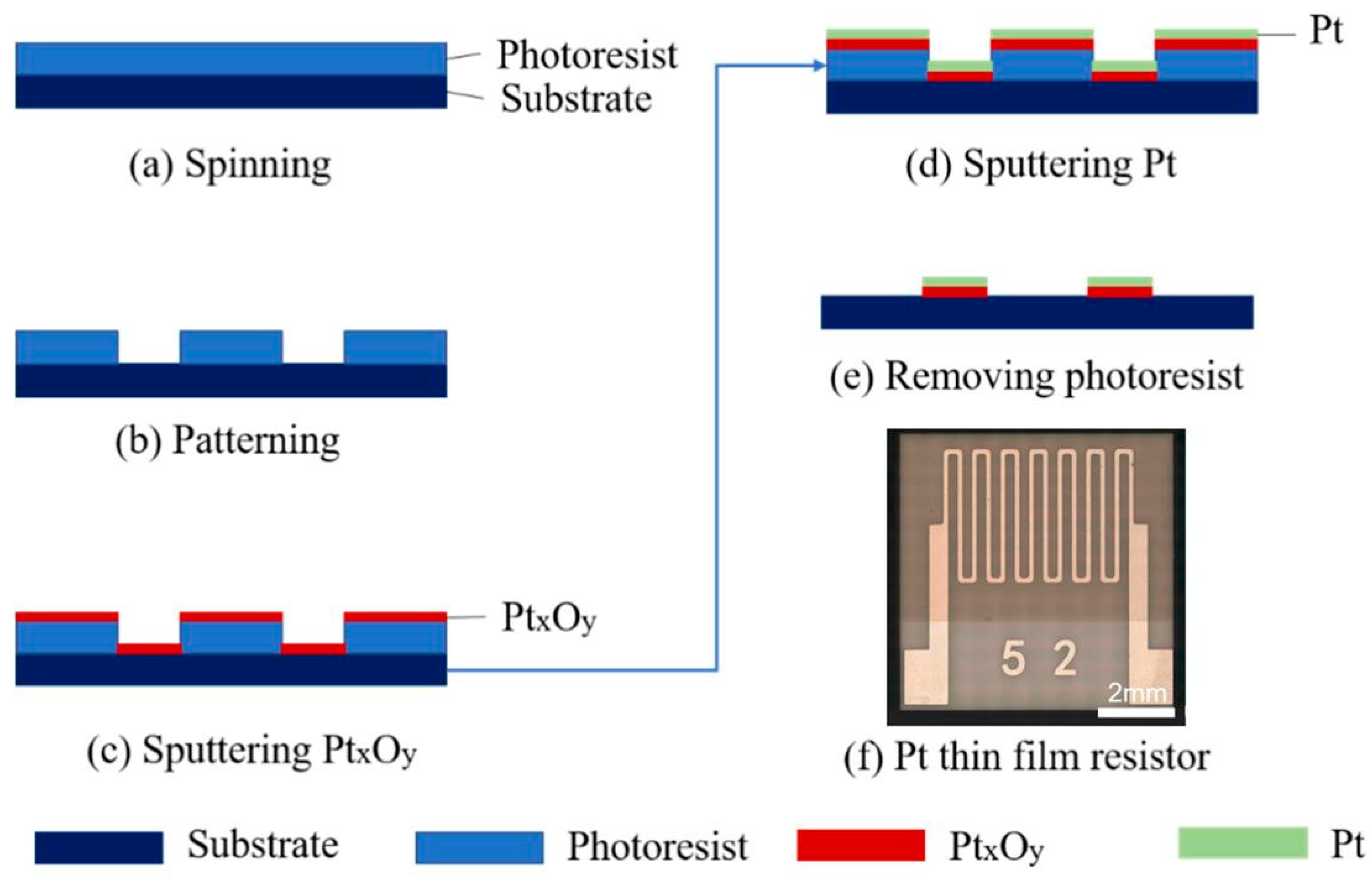
2.1. Pt Thin-Film Resistor Preparation

First of all, a 3-inch-diameter single-polished alumina ceramic substrate was cleaned with nanometer calcium carbonate to ensure uniform grinding in all areas, followed by rinsing with deionized water, so that the water can be completely wetted; there were no aggregated water droplets on the surface; the process was correspondingly followed by ultrasonic cleaning with deionized water, 5% sodium hydroxide, and potassium dichromate solution. Then the Pt thin-film resistor was fabricated by microlithography and lift-off process. The process schematic was given in Figure 1a–e. A positive photoresist of AZ-4620 was spin-coated onto the alumina substrate and baked at 90 °C for 2 h. The resistor pattern was transferred after exposure for 40 s under the i-line from a mercury arc lamp with a constant intensity of 8 mW.cm−2. The substrate was then immersed in a developer solution. Afterward, the substrate was rinsed with deionized water to remove the remaining developer and then baked at 90 °C for 30 min.
The PtxOy adhesion layer was deposited by reactive magnetron sputtering (MSP-400, China) using a Pt target (99.99%) with a diameter of 100 mm in O2/Ar gas mixtures with an oxygen partial pressure ranging from 5% to 50%. Then, a Pt film was deposited by radio frequency (RF) sputtering in pure Ar atmosphere. The base and sputtering pressures were 5 × 10⁻⁴ Pa and 0.5 Pa, respectively. The PtxOy adhesion layer and Pt film have the same sputtering power of 150 W and different depositing times of 5 min and 8 min, respectively. The deposition rates of various oxygen partial pressures are listed in Table 1. Pt/PtxOy films were structured by a lift-off process. After being rinsed with deionized water and dried with N2, the substrate was cut into several small pieces (7.5 mm × 7.1 mm × 0.6 mm) by laser cutting equipment, as illustrated in Figure 1f. The Pt RTDs were annealed in a muffle furnace at different temperatures (800–1000 °C) for 2 h with a heating rate of 5 °C/min and then naturally cooled.

2.2. Characterization of Resistor

(1) Digital microscopy (Keyence, VHX-5000, Japan), scanning electron microscopy (SEM, Zeiss Ultra55, Germany), and focused ion beam (FIB, Zeiss Auriga SEM/FIB crossbeam System, Germany) were used to characterize the surface and cross-sectional microstructure. Polyfunctional X-ray diffraction (XRD, Bruker 3 kW/D8 ADVANCE Da Vinci, Germany) was applied to measure crystallinity and full width at half-maximum (FWHM) with Cu Kα radiation (λ = 1.5406 Å) operated at 40 kV and 40 mA. X-ray photoelectron spectroscopy (XPS) with a monochromatic Al Kα source (1486.6 eV) was used to characterize the surface chemical composition of the Pt film. Pass energies of 160 eV and 40 eV were used for survey spectra and narrow scan spectra with energy step sizes of 1 eV and 0.1 eV, respectively. The binding energy scale was calibrated according to the C 1s peak (284.8 eV) of adventitious carbon on the analyzed sample surface. Time-of-flight secondary ion mass spectrometry (TOF-SIMS, ION TOF TOF-SIMS 5-100, Germany) was used to characterize the three-dimensional and spatial scale chemical composition distribution.
(2) For a standard Pt100 resistor, the dependence of resistance on temperature was described as follows:
R T = R 0 1 + A T + B T 2 0   ° C < T < 850   ° C
where A and B were fitting constants, and R0 was the resistance at 0 °C. At low temperature (0–200 °C), B was negligible because the resistance temperature curve (R–T curve) had high linearity with a coefficient of determination of linear regression greater than 0.9999.
The average TCR was calculated as follows:
T C R = α = ( R T 2 R T 1 ) / ( R T 1 · ( T 2 T 1 ) ) = R / T · R T 1
where ∆R/∆T was the slope of the R–T curve, and RT1 corresponded to the resistance at 20 °C. It should be noted that this R–T curve referred to the first temperature test for the annealed resistor. To obtain the temperature dependence of the resistance, each resistor was measured by a 61/2 digital Agilent multimeter (Agilent, Keysight 34464A, USA), and the resistor temperature was controlled by an intelligent thermostatic oil bath with methyl silicone as the medium between 20 and 150 °C. The heating rate of the intelligent thermostatic oil bath was approximately 2 °C/min. The temperature was raised in increments of 10 °C and held for 5 min after each increase. During the holding time, the data were recorded.
The stability of the resistor was characterized by the change rate of RT1 after 4 tests of R–T curves. The R–T curve was obtained through a data acquisition system (Agilent, Keysight DAQ970A, USA) and muffle furnace at test temperatures from room temperature to 800 °C with a heating rate of 5 °C/min. In the testing process, the muffle is used to provide a high-temperature environment, the R-type thermocouple is used to calibrate the furnace temperature, and the Pt RTDs’ resistance is output through DAQ970A.

3. Results and Discussion

We prepared the PtxOy adhesion layer made with oxygen partial pressures of 5%, 10%, 15%, 20%, and 50% and then annealed in a muffle furnace up to 800 °C, 900 °C, and 1000 °C for 2 h to investigate the influential mechanisms of oxygen partial pressure and annealing temperature.

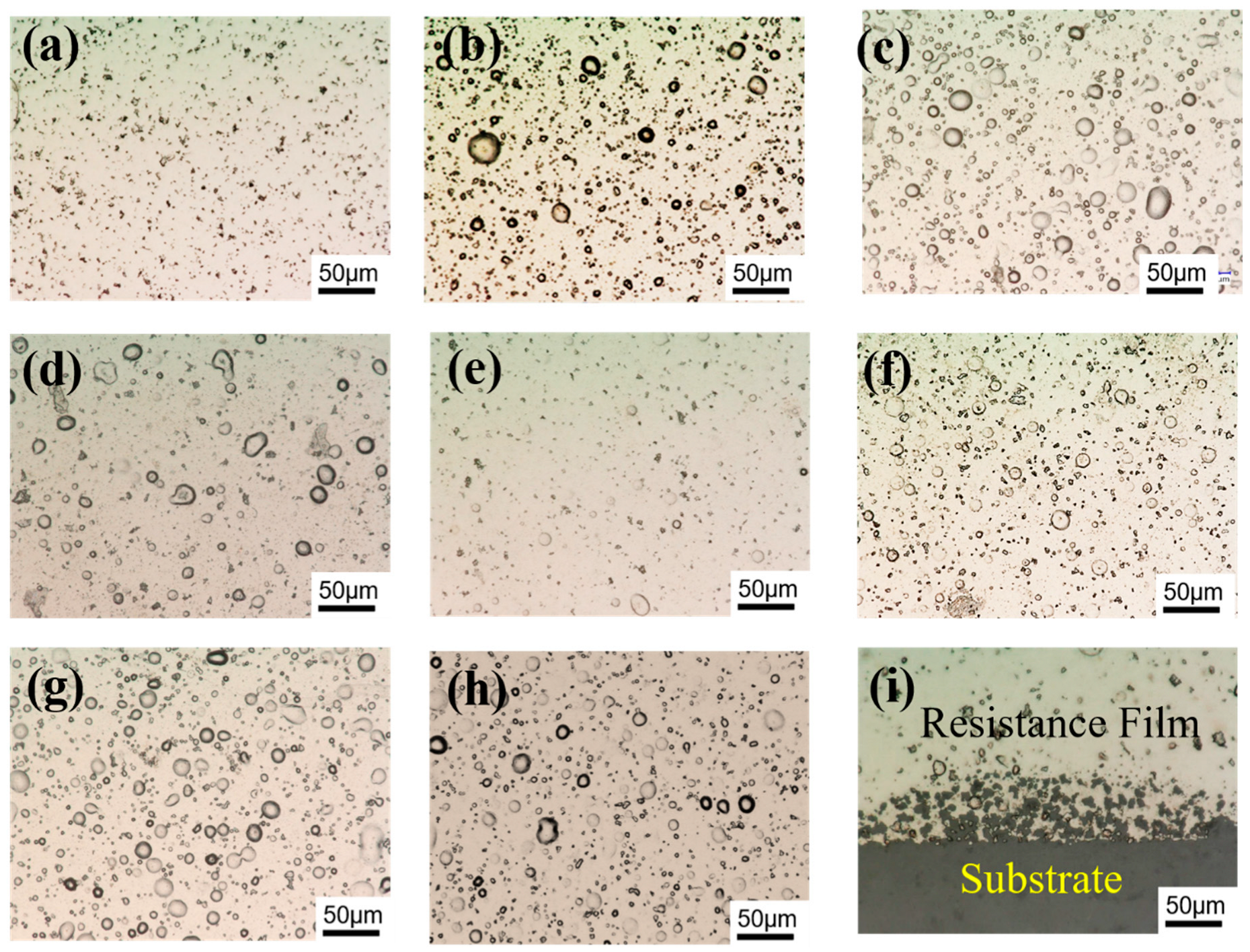
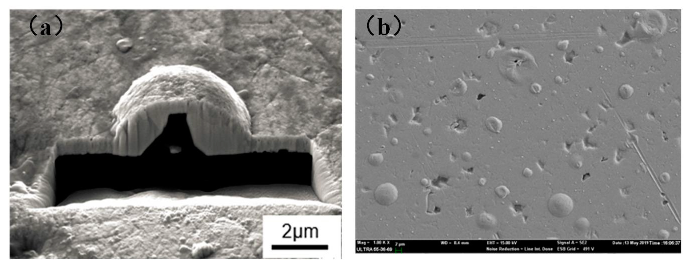
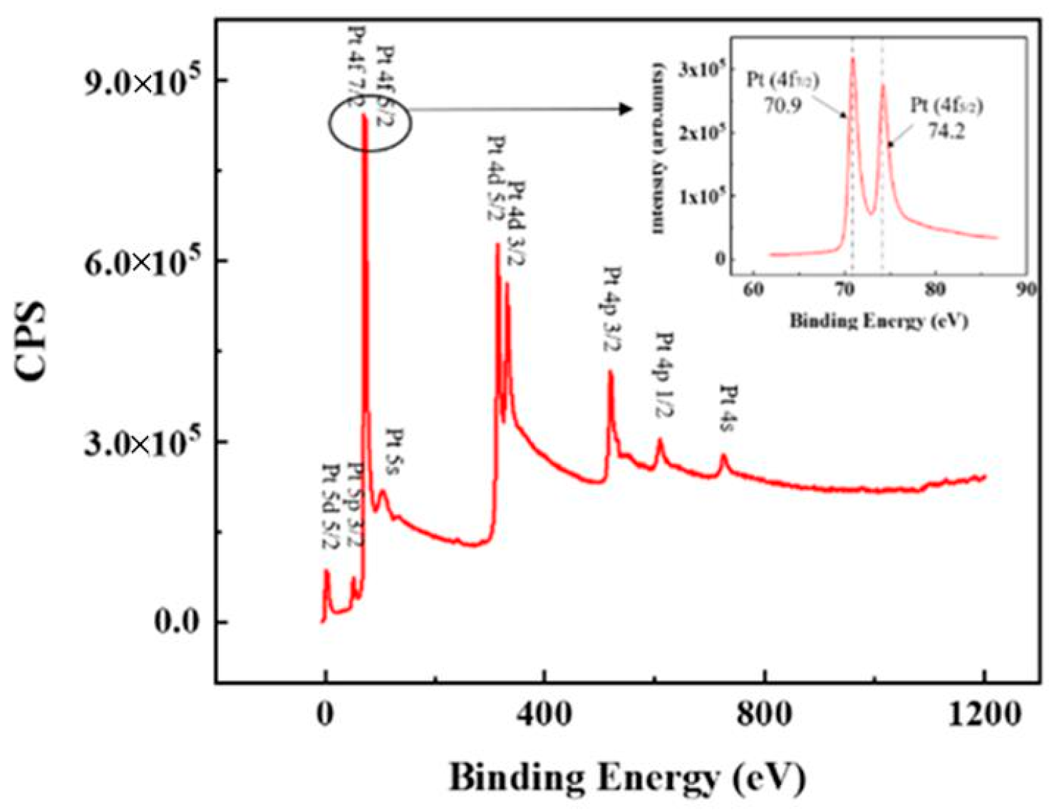
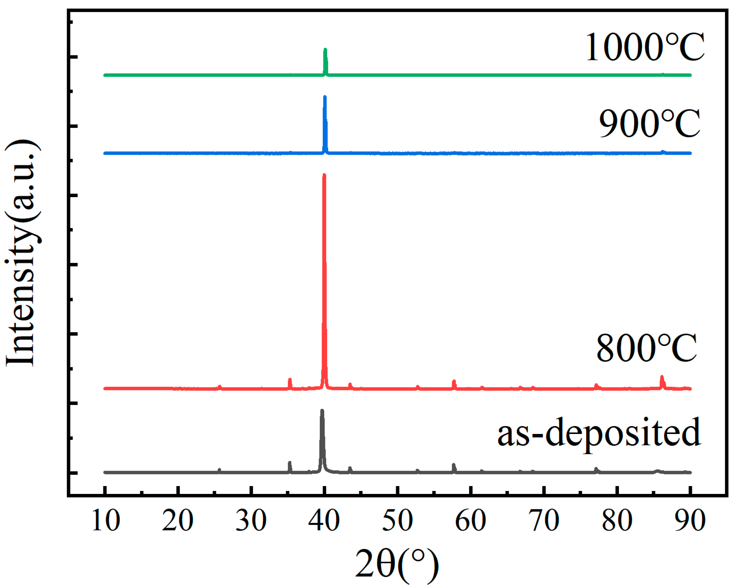
3.1. Microstructure and Chemical Composition

The morphologies of the as-deposited and annealed Pt/PtxOy/Al2O3 resistors with different oxygen partial pressure and annealed temperature in the adhesion layer are shown in Figure 2 [24].
Figure 2a shows that the defects on the surface of the as-deposited film were caused by rough substrates. Compared with the as-deposited films, blisters with diameters in the range of 2 μm to 20 μm were observed, and they were irregularly distributed on the surface of the annealed films. As the oxygen partial pressure increased from 5% (Figure 2b) to 10% (Figure 2c), the number of bumps sharply increased. When the oxygen partial pressure increased from 15% to 50%(Figure 2d–f), the blisters that formed on the surface of the Pt film significantly decreased. At an oxygen partial pressure of 15% (Figure 2d), the number of bumps drastically decreased compared with that at 10%. When the oxygen partial pressure increased to 20% (Figure 2e), the bumps were almost unnoticeable. As the oxygen partial pressure increased to 50% (Figure 2f), there were some bumps on the surface of the Pt/PtxOy film. Kwon et al. and Hummel et al. also observed blisters in the Pt film, and they assumed that the formation of bubbles is due to the Ar collection at the film–substrate interface. However, the diffusion of Ar atoms over the micron-scale distances required to collect Ar at a blister location seems unlikely. Compared with Figure 2a, there is no blister formation.
For a given oxygen partial, as the annealing temperature increased from 800 °C to 1000 °C (Figure 2c,g,h), the number of blisters first increased and then decreased. The above phenomenon can be explained that with the increase in the annealing temperature, the decomposition of PtxOy intensifies, more O2 escapes, and the number of bubbles on the surface of the thin film increases. As the annealing temperature continued to increase, the PtxOy content decreased and the decomposition weakened. As the grain size increased, the defects were eliminated, and the bubbles were repaired due to the grain growth; then the number of bubbles decreased.
Figure 2i showed the edge of the Pt/PtxOy film annealed at 1000 °C. Film agglomeration and voids were observed, which agreed with the phenomena reported in previous research. It was reported that the capillary action produced by the high specific surface area of the film was the main reason for the agglomeration. Films always have defects or pinholes [25]. When the radius of the defect was larger than the thermodynamic critical radius determined by the film thickness and wetting angle, the defect grew through capillary action until it was stable [26,27]. Longer exposure time and higher temperature would increase agglomeration, which increased the resistance and was harmful for devices [25,28].
The cross-section morphologies of a blister are shown in Figure 3a. The wall thickness was not uniform, and a gap (~2 μm) was formed between the film and substrate, which may be due to gas escape during annealing. The PtxOy adhesion layer prepared by reactive RF sputtering was composed of Pt, PtO, and PtO2. Earlier studies indicated that PtO2 began to break down at 550 °C to form O2, PtO, and Pt. PtO2 and PtO continued to decompose into Pt and O2 with increasing temperature [28], and all Pt–O compounds completely dissociated into Pt at 1100 °C [29,30]. Therefore, the blisters may be caused by the decomposition of the PtxOy adhesion layer and oxygen escape. The focused ion beam (FIB) results of the surface are shown in Figure 3b.
Figure 4 showed the wide scan and Pt XPS spectra of the as-deposited Pt/PtxOy film. The binding energies of the Pt 4f7/2 and Pt 4f5/2 peaks were 70.9 eV and 74.2 eV, respectively, which agreed with the reported values of 70.3 eV and 73.68 eV for a pure Pt film [19]. It is verified that the upper layer of the Pt/PtxOy/Al2O3 resistor was Pt.
To test our assumption of blisters resulting from the decomposition of PtxOy, TOF-SIMS depth profiling experiments were conducted on the as-deposited and annealed Pt/PtxOy/Al2O3 resistors with the adhesion layer prepared with 10% oxygen partial pressure. The depth profiling plots and 3D rendered images of ions Pt, PtO, PtO2, and AlO for the as-deposited and annealed films were constructed from raw data and are given in Figure 5.
Figure 5a showed the peak intensity changes of ions (Pt, PtO, PtO2−, and AlO) with the sputtering time that corresponded to the depth, and the longer the sputtering time was, the deeper the depth was. Pt ions represented the existence of Pt-containing materials, such as metallic Pt and platinum oxide, while PtO and PtO2 ions indicated the presence of a platinum oxide layer, and the AlO ion represented the Al2O3 substrate. From Figure 5a, the interface of the resistance film and Al2O3 substrate was clear at a sputtering time of approximately 1860 s, and the PtxOy adhesion layer was located at a depth reached between approximately 1500 s and 1860 s; then sputtering time from 0 s to approximately 1500 s corresponded to Pt. This suggested that there is a PtxOy adhesion layer between the Pt film and Al2O3 substrate, forming a sandwich structure of Pt/PtxOy/Al2O3, which was more directly revealed by the 3D rendering images in Figure 5b.
For the annealed films, as shown in Figure 5c,e,g, the PtO2 and PtO ion peak intensities and their distribution widths were much lower and wider than those of the as-deposited film (Figure 5a), indicating that the annealing thins the PtxOy adhesion layer and intensifies the diffusion. This phenomenon could also be easily found from Figure 5b,d,h. Additionally, AlO ions appeared to penetrate the upper Pt layer after annealing, as Figure 5d shows, which suggested that Al2O3 will diffuse to Pt. With increasing annealing temperature, the intensity of PtO2 and PtO first decreased and then slightly increased, and the interface of the PtxOy adhesion layer gradually blurred.
X-ray diffraction pattern of the as-deposited and annealed resistance films was obtained, as illustrated in Figure 6. Compared with the as-deposited film, the spectra showed an obvious increase in the intensity of the Pt (111) peak in the 800 °C annealed resistance film, which revealed an increase in crystallinity. With increasing annealing temperature, Pt oxidation got serious and the lattice constant decreased, which caused the Pt (111) peak to shift to a larger 2θ.
In addition, oxidation, film heat loss, agglomeration, and diffusion contributed to the drastic reduction in the intensity of the Pt (111) peak. The FWHMs of the Pt (111) peak in the as-deposited resistance film and resistance films annealed at 800 °C, 900 °C, and 1000 °C were evaluated as 0.290°, 0.136°, 0.094°, and 0.116°, which indicated that grain growth occurred as the annealing temperature increased.

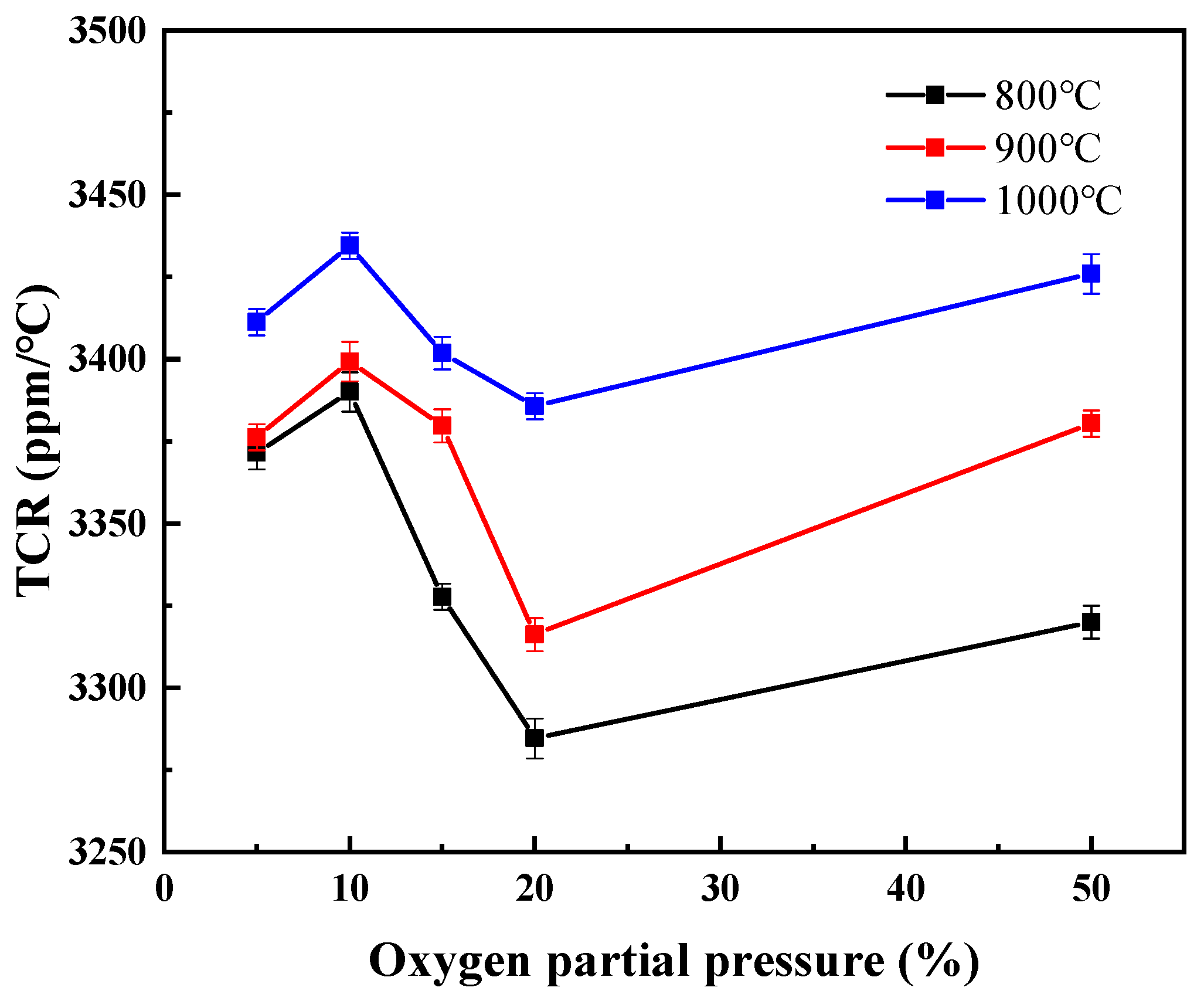
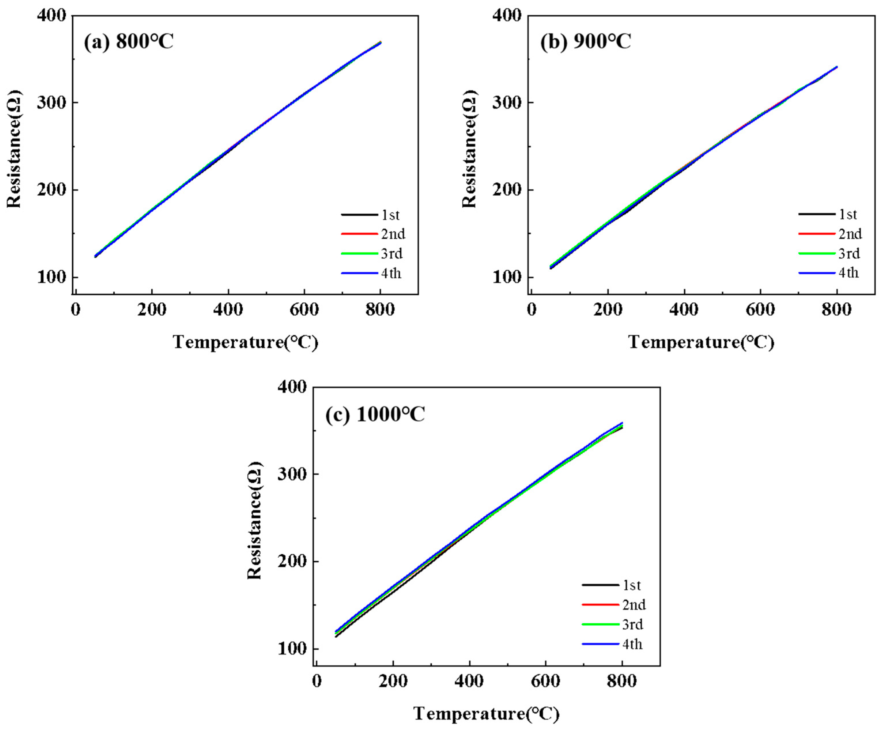
3.2. Electrical Properties and High-Temperature Stability

To investigate the effect of oxygen partial pressure and annealing temperature on the Pt RTDs’ electrical properties, the resistance change rate was investigated, as shown in Table 2. It should be noted that due to experimental error, the resistance of resistors fabricated by the same process on the same substrate is not the same, and the standard deviation is about 10 Ω. In this work, resistors with similar resistances (±5 Ω) were selected for testing, and the test results were the average of 5 specimens.
With increasing oxygen partial pressure, the initial resistance of the as-deposited resistors first increased and then decreased. The resistance decreased after annealing, and the larger the oxygen partial pressure was, the more the resistance decreased. For Pt/PtxOy/Al2O3 resistors prepared with fixed oxygen partial pressure, the annealing temperature has little effect on the rate of resistance change. Resistors with an adhesion layer prepared with 10% oxygen partial pressure showed the most stable change rate in the entire annealing temperature range.
The TCR is a key parameter for characterizing Pt resistance. There are many parameters that influence the TCR, such as crystal characteristics, void formation, the nature of the substrate, interdiffusion of adhesion layers, etc. [31,32]. Figure 7 depicts the TCR versus oxygen partial pressure and annealing temperature. Error bars represented the standard deviation. The TCR increased with increasing annealing temperature but did not monotonically vary with an increase in the oxygen partial pressure. The variation trend of resistors annealed at different temperatures was similar. For example, at 800 °C, the TCR increased from 3371 ppm/°C to 3390 ppm/°C as the oxygen partial pressure increased from 5% to 10%. When the oxygen partial pressure increased further, however, the TCR began to decrease. For resistors with an adhesion layer prepared with 15% oxygen partial pressure, the TCR was 3327 ppm/°C, and when the oxygen partial pressure was raised to 20%, it dropped to 3285 ppm/°C due to large resistance. As it increased to 50%, the TCR returned to 3320 ppm/°C. The largest TCR was 3434 ppm/°C, which corresponded to the Pt thin-film resistors with an adhesion layer prepared with 10% oxygen partial pressure and annealed at 1000 °C. It can be explained that with increasing oxygen partial pressure, the PtxOy content in the adhesion layer increased, which directly led to an increase in resistance. Although PtxOy decomposed during annealing, there was still a considerable amount of PtxOy when oxygen partial pressure was above 10%, and the resistance was large, leading to a small TCR. On the other hand, a high oxygen concentration in sputtering was harmful due to more anomalies and discoloration [21], which resulted in an increase in resistivity and a decrease in the TCR because the product of resistivity and the TCR was constant [33]. The unexpected phenomenon of the resistor with an adhesion layer prepared with 50% oxygen partial pressure was not clear and may be related to the oxidation of Pt in the target surface becoming saturated.
Stability is an important performance parameter for thin-film resistors. The R–T curves of resistors with an adhesion layer prepared with 10% oxygen partial pressure and annealed at 800 °C, 900 °C, and 1000 °C were tested. Resistance operating temperature should not be higher than annealing temperature. Based on this, each test was carried out for 4 cycles up to 800 °C, and the curves are shown in Figure 8.
The resistance of all resistors slightly increased with the change rates of 0.14%, 0.13%, and 0.4%, corresponding to resistors annealed at 800 °C, 900 °C, and 1000 °C, respectively. It was clear that the R–T curves of resistors annealed at 800 °C and 900 °C had better repeatability than those of resistors annealed at 1000 °C, which showed an obvious shift as the experiment proceeded. Then we can conduct that the resistor prepared with an oxygen partial pressure of 10% and annealed at 900 °C owned a high TCR and good stability.

4. Conclusions

For Pt thin-film resistors with a PtxOy adhesion layer, the influence of the annealing temperature (800 °C, 900 °C, and 1000 °C) and oxygen partial pressure (5%, 10%, 15%, 20%, and 50%) on the film microstructure, electrical properties, stability, and film adhesion was investigated. Then the Pt thin-film resistor was fabricated by microlithography and lift-off process and prepared by reactive magnetron sputtering. After annealing, PtxOy decomposed and bubbles formed on the surface of the Pt thin film. In addition, the resistance decreased after annealing, and the higher the oxygen partial pressure was, the greater the resistance decreased. The Pt thin-film resistor with a PtxOy adhesion layer sputtered at 10% oxygen partial pressure and annealed at 1000 °C had the largest TCR (3434 ppm/°C). The resistors annealed at 800 °C and 900 °C had better stability than those annealed at 1000 °C. The PtxOy adhesion layer increased film adhesion through oxygen-to-oxygen bonding. Overall, for better properties, the optimal oxygen partial pressure and annealing temperature were 10% and 900 °C, respectively. Further improvement can be achieved by protective layers, such as glazes, aluminum oxide, and so on to reduce agglomeration and film loss at high temperature.

Author Contributions

Conceptualization, Y.P. and C.Z.; methodology, Y.P.; validation, Y.P., N.Z., L.S. and Y.R.; formal analysis, N.Z. and Y.R.; investigation, Y.P.; resources, Y.R. and C.Z.; data curation, Y.R. and N.Z.; writing—original draft preparation, Y.P.; writing—review and editing, N.Z.; visualization, L.S. and Y.R.; supervision, Y.R.; project administration, C.Z.; funding acquisition, C.Z. All authors have read and agreed to the published version of the manuscript.

Funding

This research was funded by the National Key Research and Development Program of China [2020YFB2009102].

Institutional Review Board Statement

Not applicable.

Informed Consent Statement

Not applicable.

Data Availability Statement

Not applicable.

Acknowledgments

The authors thank the Shanghai Electric Institute and School of Naval Architecture, Ocean & Civil Engineering for film adhesion testing experiments, the Center for Advanced Electronic Material and Devices for SEM and XRD measurement, and Limin Sun in the Instrumental Analysis Center of Shanghai Jiao Tong University for TOF-SIMS characterization.

Conflicts of Interest

The authors declare no conflict of interest.

References

  1. Li, M.; Hu, T. Research status and development trend of MEMS S&A devices: A review. Def. Technol. 2020, 17, 450–456. [Google Scholar]
  2. Lin, X.; Zhang, C.; Yang, S.; Guo, W.; Zhang, Y.; Yang, Z.; Ding, G. The impact of thermal annealing on the temperature dependent resistance behavior of Pt thin films sputtered on Si and Al2O3 substrates. Thin Solid Film. 2019, 685, 372–378. [Google Scholar] [CrossRef]
  3. Zhao, X.; Yan, S.; Wang, H.; Jiang, H.; Zhang, W. Fabrication and microstructure evolution of Al2O3/ZrBN-SiCN/Al2O3 high-temperature oxidation-resistant composite coating. Ceram. Int. 2019, 45, 247–251. [Google Scholar] [CrossRef]
  4. Tsutsumi, K.; Yamashita, A.; Ohji, H. The experimental study of high TCR Pt thin films for thermal sensors. In Proceedings of the Sensors, 2002 IEEE, Orlando, FL, USA, 12–14 June 2002; pp. 1002–1005. [Google Scholar]
  5. Purkl, F.; English, T.; Yama, G.; Provine, J.; Kenny, T.W. Sub-10 nanometer uncooled platinum bolometers via plasma enhanced atomic layer deposition. In Proceedings of the IEEE International Conference on Micro Electro Mechanical Systems, Taipei, Taiwan, 20–24 January 2013. [Google Scholar]
  6. Rusanov, R.; Rank, H.; Fuchs, T.; Mueller-Fiedler, R.; Kraft, O. Reliability characterization of a soot particle sensor in terms of stress- and electromigration in thin-film platinum. Microsyst. Technol. 2016, 22, 481–493. (In English) [Google Scholar] [CrossRef]
  7. Fricke, S.; Friedberger, A.; Seidel, H.; Schmid, U. A robust pressure sensor for harsh environmental applications. Sens. Actuators A Phys. 2012, 184, 16–21. [Google Scholar] [CrossRef]
  8. Mattox, D.M. Influence of Oxygen on the Adherence of Gold Films to Oxide Substrates. J. Appl. Phys. 1966, 37, 3613–3615. [Google Scholar] [CrossRef]
  9. Schmidl, G.; Dellith, J.; Kessler, E.; Schinkel, U. The influence of deposition parameters on Ti/Pt film growth by confocal sputtering and the temperature dependent resistance behavior using SiOx and Al2O3 substrates. Appl. Surf. Sci. 2014, 313, 267–275. [Google Scholar] [CrossRef]
  10. Sreenivas, K.; Reaney, I.; Maeder, T.; Setter, N.; Jagadish, C.; Elliman, R.G. Investigation of Pt/Ti bilayer metallization on silicon for ferroelectric thin film integration. J. Appl. Phys. 1994, 75, 232–239. [Google Scholar] [CrossRef]
  11. Weng, S.; Qiao, L.; Wang, P. Thermal stability of Pt-Ti bilayer films annealing in vacuum and ambient atmosphere. Appl. Surf. Sci. A J. Devoted Prop. Interfaces Relat. Synth. Behav. Mater. 2018, 444, 721–728. [Google Scholar] [CrossRef]
  12. Martin, D.M.; Agham, P.; Thong, Q.N.; Ajit, D.; David, J.S.; Alexander, A.D.; John, G.E. Growth of epitaxial oxides on silicon using atomic layer deposition: Crystallization and annealing of TiO2 on SrTiO3-buffered Si(001). J. Vac. Sci. Technol. B. Nanotechnol. Microelectron. Mater. Process. Meas. Phenom. JVST B 2012, 30, 04E111-1–04E111-6. (In English) [Google Scholar]
  13. Halder, S.; Schneller, T.; Waser, R. Enhanced stability of platinized silicon substrates using an unconventional adhesion layer deposited by CSD for high temperature dielectric thin film deposition. Appl. Phys. A. Mater. Sci. Process. 2007, 87, 705–708. (In English) [Google Scholar] [CrossRef]
  14. Ababneh, A.; Al-Omari, A.N.; Dagamseh, A.M.K.; Tantawi, M.; Pauly, C.; Mücklich, F.; Feili, D.; Seidel, H. Electrical and morphological characterization of platinum thin-films with various adhesion layers for high temperature applications. Microsyst. Technol. 2015, 23, 703–709. [Google Scholar] [CrossRef]
  15. Schmid, U.; Seidel, H. Effect of high temperature annealing on the electrical performance of titanium/platinum thin films. Thin Solid Films 2008, 516, 898–906. [Google Scholar] [CrossRef]
  16. Courbat, J.; Briand, D.; Rooij, N. Reliability improvement of suspended platinum-based micro-heating elements. Sens. Actuators A Phys. 2008, 142, 284–291. [Google Scholar] [CrossRef]
  17. Garraud, A.; Combette, P.; Giani, A. Thermal stability of Pt/Cr and Pt/Cr2O3 thin-film layers on a SiNx/Si substrate for thermal sensor applications. Thin Solid Films 2013, 540, 256–260. [Google Scholar] [CrossRef]
  18. Chung, G.S.; Kim, C.H. RTD characteristics for micro-thermal sensors. Microelectron. J. 2008, 39, 1560–1563. [Google Scholar] [CrossRef]
  19. Kuribayashi, K.; Kitamura, S. Preparation of Pt-PtOx thin films as electrode for memory capacitors. Thin Solid Films 2001, 400, 160–164. [Google Scholar] [CrossRef]
  20. Budhani, R.C.; Prakash, S.; Bunshah, R.F. Thin-film temperature sensors for gas turbine engines: Problems and prospects. J. Vac. Sci. Technol. A Vac. Surf. Film. 1986, 4, 2609–2617. [Google Scholar] [CrossRef]
  21. John, D.W.; Kimala, L.H. Preparation and Analysis of Platinum Thin Films for High Temperature Sensor Applications; National Aeronautic Space Administration (NASA): Washington, DC, USA, 2005. [Google Scholar]
  22. Grosser, M.; Schmid, U. The impact of annealing temperature and time on the electrical performance of Ti/Pt thin films. Appl. Surf. Sci. 2010, 256, 4564–4569. [Google Scholar] [CrossRef]
  23. Schssler, T.; Schn, F.; Lemier, C.; Urban, G. Effect of high temperature annealing on resistivity and temperature coefficient of resistance of sputtered platinum thin films of SiO2/Pt/SiOx interfaces. Thin Solid Films 2020, 698, 137877. [Google Scholar] [CrossRef]
  24. Pang, Y.; Zhang, C.; Lei, P.; Wang, Y.; Lv, Z. Effects of Thermal Annealing on the Electrical Properties and Stability of Pt Thin Film Resistors with Ti and PtxOy Interlayers. J. Phys. Conf. Ser. 2021, 2002, 012002. [Google Scholar] [CrossRef]
  25. Firebaugh, S.L.; Jensen, K.F.; Schmidt, M.A. Investigation of high-temperature degradation of platinum thin films with an in situ resistance measurement apparatus. J. Microelectr. Syst. 1998, 7, 128–135. [Google Scholar] [CrossRef]
  26. Jiran, E.; Carl, V. Thompson. Capillary instabilities in thin films. J. Electron. Mater. 1990, 19, 1153–1160. [Google Scholar] [CrossRef]
  27. Berry, R.J. Effect of Pt Oxidation on Pt Resistance Thermometry. Metrologia 1980, 16, 117–126. [Google Scholar] [CrossRef]
  28. Niu, Y.L.; Song, K.; Sun, J.P.; Xu, L.I.; Meng, Y.E. Research on the Decomposition Experiment of PtO2 in Air Environment. Acta Metrol. Sin. 2018, 39, 33–38. [Google Scholar]
  29. Mooiman, M.B.; Sole, K.C.; Dinham, N. The Precious Metals Industry: Global Challenges, Responses, and Prospects. In Metal Sustainability: Global Challenges, Consequences, and Prospects; John Wiley & Sons, Ltd.: Hoboken, NJ, USA, 2016. [Google Scholar]
  30. Joseph, R.D. Precious Metals and Alloys. In Metals Handbook Desk Edition; ASM International: Almere, The Netherlands, 1998. [Google Scholar] [CrossRef]
  31. Kumar, M.; Kumar, T.; Pandey, R.K.; Pathak, S.; Kumar, R. Roughening and Sputtering Kinetics of Pt Thin Films at different Angles of Ion Irradiation. Mater. Lett. 2021, 303, 130474. [Google Scholar] [CrossRef]
  32. Ruina, J.; Kunlun, W.; Yanqing, X.; Hui, S.; Jianhong, G.; Lan, Y.; Yong, W. Enhancing the temperature coefficient of resistance of Pt thin film resistance-temperature-detector by short-time annealing. Ceram. Int. 2023, 49, 12596–12603. [Google Scholar]
  33. Zhang, Y.; Ba, D.; Liu, X.; Hang, G. Latest Progress in Development of Thin Film Temperature Sensors. Vac. Sci. Technol. 2003, 23, 334–1124. [Google Scholar]
Figure 1. Fabrication process (ae) and overall morphology (f) of Pt thin-film resistor.
Chemosensors 11 00285 g001
Figure 2. (a) Morphologies of the as-deposited resistance film and resistance films with adhesion layer prepared with oxygen partial pressure of (b) 5%, (c) 10%, (d) 15%, (e) 20%, and (f) 50% annealed at 800 °C. Resistance films prepared with 10% oxygen partial pressure in the adhesion layer annealed at (g) 900 °C and (h) 1000 °C. (i) Edge of (h) [24].
Chemosensors 11 00285 g002
Figure 3. (a) Cross-section of a blister; (b) FIB of surface.
Chemosensors 11 00285 g003
Figure 4. Wide scan and Pt XPS spectra of the as-deposited Pt/PtxOy film.
Chemosensors 11 00285 g004
Figure 5. Depth profiling plots (a,c,e,g) and 3D rendered images (b,d,f,h) of ions Pt, PtO, PtO2, and AlO for the as-deposited resistance films (a,b) and resistance films annealed at 800 °C (c,d), 900 °C (e,f), and 1000 °C (g,h).
Chemosensors 11 00285 g005
Figure 6. X-ray diffractograms of the as-deposited and annealed resistance films.
Chemosensors 11 00285 g006
Figure 7. TCR curves of Pt/PtxOy/Al2O3 resistors annealed at 800 °C, 900 °C, and 1000 °C for 2 h.
Chemosensors 11 00285 g007
Figure 8. R–T curves of Pt/PtxOy/Al2O3 resistors with adhesion layer prepared with 10% oxygen partial pressure annealed at 800 °C (a), 900 °C (b), and 1000 °C (c).
Chemosensors 11 00285 g008
Table 1. Deposition rate of PtxOy and Pt film adhesion layer prepared with various oxygen partial pressures.
FilmPtxOy Adhesion LayerPt Film
Oxygen partial pressure5%10%15%20%50%-
Deposition rate (nm/min)33 ± 434 ± 336 ± 355 ± 360 ± 448 ± 3
Table 2. Effects of oxygen partial pressure and annealing temperature on Pt/PtxOy/Al2O3 resistors.
Oxygen Partial Pressure5%10%15%20%50%
Resistance at RT
(as-deposited) (Ω)
130.6 ± 3.5146.9 ± 4.3177.5 ± 4.3196.3 ± 4.8155.4 ± 4.6
Annealing temperature and resistance change rate800 °C−19.8%−32.4%−41.0%−45.9%−47.9%
900 °C−19.0%−32.9%−34.3%−44.9%−49.0%
1000 °C−17.6%−32.6%−34.1%−43.7%−49.1%
Note: All resistance change rate had standard deviation less than 0.03.
Disclaimer/Publisher’s Note: The statements, opinions and data contained in all publications are solely those of the individual author(s) and contributor(s) and not of MDPI and/or the editor(s). MDPI and/or the editor(s) disclaim responsibility for any injury to people or property resulting from any ideas, methods, instructions or products referred to in the content.

