
Improving Surface Imprinting Effect by Reducing Nonspecific Adsorption on Non-Imprinted Polymer Films for 2,4-D Herbicide Sensors


1
School of Applied Chemical Engineering, Kyungpook National University, 80 Daehak-ro, Buk-gu, Daegu 41566, Korea
2
Department of Cogno-Mechatronics Engineering, Department of Optics and Mechatronics Engineering, College of Nanoscience and Nanotechnology, Pusan National University, Busan 46241, Korea
3
Department of Polymer Science & Engineering, Kyungpook National University, 80 Daehak-ro, Buk-gu, Daegu 41566, Korea
*
Authors to whom correspondence should be addressed.
Chemosensors 2021, 9(3), 43; https://doi.org/10.3390/chemosensors9030043
Submission received: 6 February 2021
/
Revised: 23 February 2021
/
Accepted: 24 February 2021
/
Published: 26 February 2021
(This article belongs to the Special Issue Recent Advances in Quartz Crystal Microbalance-Based Sensor Applications)
Abstract
:Surface imprinting used for template recognition in nanocavities can be controlled and improved by surface morphological changes. Generally, the lithographic technique is used for surface patterning concerning sensing signal amplification in molecularly imprinted polymer (MIP) thin films. In this paper, we describe the effects of silanized silica molds on sensing the properties of MIP films. Porous imprinted poly(MAA–co–EGDMA) films were lithographically fabricated using silanized or non-treated normal silica replica molds to detect 2,4-dichlorophenoxyacetic acid (2,4-D) herbicide as the standard template. The silanized mold MIP film (st-MIP) (Δf = −1021 Hz) exhibited a better sensing response than the non-treated normal MIP (n-MIP) (Δf = −978 Hz) because the imprinting effects, which occurred via functional groups on the silica surface, could be reduced through silane modification. Particularly, two non-imprinted (NIP) films (st-NIP and n-NIP) exhibited significantly different sensing responses. The st-NIP (Δfst-NIP = −332 Hz) films exhibited lower Δf values than the n-NIP film (Δfn-NIP = −610 Hz) owing to the remarkably reduced functionality against nonspecific adsorption. This phenomenon led to different imprinting factor (IF) values for the two MIP films (IFst-MIP = 3.38 and IFn-MIP = 1.86), which was calculated from the adsorbed 2,4-D mass per poly(MAA–co–EGDMA) unit weight (i.e., QMIP/QNIP). Moreover, it was found that the st-MIP film had better selectivity than the n-MIP film based on the sensing response of analogous herbicide solutions. As a result, it was revealed that the patterned molds’ chemical surface modification, which controls the surface functionality of imprinted films during photopolymerization, plays a role in fabricating enhanced sensing properties in patterned MIP films.
1. Introduction
The molecular imprinting technique is extensively used for various applications such as sorbents and sensors. Molecularly imprinted polymers (MIP) can be formed using this technique by undergoing a thermal/photopolymerization process between the monomers and the crosslinkers in the presence of target molecules to make mimicked cavities in the polymer matrix after template removal [1,2]. As a favorable sensing approach, molecular imprinting is widely employed as optical sensors [3], electrochemical biosensors [4], and biomimetic sensors [5,6] as well as is used for drug extraction applications [7].
Enormous effort has been invested into the development of MIP-based sensors, for example, for core–shell nanoparticles [8], lithographical patterns [9,10], and organic–inorganic hybrids [11]. Among them, the lithographic approach is an efficient tool for MIP structuring on sensing surfaces associated with quartz crystal microbalance (QCM) and could be combined with electro-/photochemical polymerization to fabricate specifically designed imprinted films. Various specific templates, from small molecules to large proteins, could be successfully imprinted on sensor platforms [12,13,14,15,16]. Recently, our group focused on increasing the sensing response of QCM-based MIP sensors by controlling the surface area of MIP films, which were fabricated using colloidal/soft lithography and photo-/electropolymerization [17]. Compared to their planar MIP film counterparts, the structured MIP films exhibited enhanced sensing signal response during a limited period owing to the increased surface area into which the specific template diffused in solution. The use of a poly(dimethylsiloxane) (PDMS) replica mold is a ubiquitous lithographic tool for generating MIP films during photopolymerization. However, pre-curing of the MIP precursor solution is required to prevent functional monomers, templates, and crosslinkers from being absorbed into the molds. Moreover, polystyrene (PS) or silica colloids can be used as a master mold to fabricate convex or concave hemispherical patterns [18]. Despite these lithographic approaches, the occurrence of undesirable nonspecific adsorption on non-imprinted polymer (NIP) thin films seriously affects the sensing parameters (i.e., the imprinting factor (IF) and the selectivity coefficient). In the past, we reported the adsorption of 2,4-dichlorophenoxyacetic (2,4-D) molecules on a template-extracted porous MIP films, which were lithographically fabricated using the silica colloidal array (d = 500 nm) as a master mold [19]. In that study, it was revealed that the hydroxyl groups on the surfaces of the silica colloids were involved in monomer–template complex formation during the polymerization process and increased nonspecific adsorption on the surface of the MIP/NIP films, consequently resulting in lowering the imprinting effect.
Thus, solving this problem in the lithographic process necessitates a new experimental strategy to control structural conformation on the surface of the MIP film formed in contact with patterned molds under photoirradiation.
Here, we report a simple strategy to decrease nonspecific binding on the surface of MIP/NIP films, leading to improved sensing properties. To this end, the surface of the structured silica particle arrays as a mold was modified with methylsilane and 2,4-D, which was used as a standard template to manipulate porous MIP thin films during the lithographic process. Fabrication of the porous MIP systems was conducted using methacrylic acid (MAA) as the functional monomer and ethylene glycol dimethacrylate (EGDMA) as the crosslinker via polymerization during microcontact lithography under ultraviolet (UV) exposure. Using a QCM, the sensing properties of the nanopatterned MIP films obtained from the silanized silica molds were measured in situ and compared to those of the MIP films that had been prepared with a non-surface-treated silica mold. Furthermore, the two corresponding NIP films were evaluated to identify differences resulting from the use of the two molds. Finally, other analogous herbicides were employed to investigate a change in selectivity of the two MIP films.
2. Materials and Methods
2.1. Materials
PS latex microspheres (d = 1 μm, 2.5 wt% dispersion in water) with a slight anionic charge were bought from Alfa Aesar Co., Ward Hill, MA, USA. Sodium dodecyl sulfate (SDS, Sigma–Aldrich Co., St. Louis, MO, USA) was used as an anionic surfactant to generate a robust PS colloidal monolayer. The SiO2 precursor was prepared using tetraethyl orthosilicate (TEOS, 98%, reagent grade) and absolute ethanol (99.5%, analytical reagent), which were purchased from Sigma–Aldrich Co. (St. Louis, MO, USA). Trimethoxy(methyl)silane (TMMS, Tokyo Chemical Industry Co., Tokyo, Japan) was used for methylation on the surface of SiO2. MAA, 2,4-D, and EGDMA were purchased from Tokyo Chemical Industry Co. (Tokyo, Japan) to be utilized as the functional monomer, template, and crosslinker, respectively. Dimethylformamide (DMF, ≥99%, Sigma–Aldrich Co., St. Louis, MO, USA) and 2,2′-azobisisobutyronitrile (AIBN, Daejung Chemicals & Metals Co. Ltd., Siheung, South Korea) were used as the solvent and photoinitiator, respectively. Other analogous chemicals such as atrazine (Sigma–Aldrich Co., St. Louis, MO, USA), ametryn (Sigma–Aldrich Co., St. Louis, MO, USA), and (4-chloro-2-methylphenoxy) acetic acid (MCPA, Tokyo Chemical Industry Co., Tokyo, Japan) were utilized for the selectivity test. Acetic acid and methanol were obtained from Duksan Co. Ltd., Ansan, South Korea. All other chemicals were used as received.
2.2. Close-Packed Arrangement of PS Microspheres
Close-packed PS microspheres were prepared on a glass substrate as per a previously reported technique [17]. Glass substrates were ultrasonicated for 5 min in acetone, ethanol, and DI water, sequentially, and dried under nitrogen (N2) gas. Next, these substrates were immersed in a piranha mixture (H2SO4:H2O2, 3:1 v/v) for 40 min to remove all impurities. A small quantity of the PS dispersion (80 μL) was diffused on the cleaned substrate using a micropipette and spin-coated with 300 rpm for 5 min via a spin-coater (BGK, NSF-100DP). The randomly arranged PS microspheres on the substrate were floated carefully onto SDS assembled on an air/water interface in a Petri-dish. In this process, the PS microspheres were closely packed using an SDS aqueous solution of 200 μL (2 wt%). Finally, the monolayer was transferred onto the glass substrate (≈2.5 × 2.5 cm2) and allowed to dry completely for a day.
2.3. Porous Hexagonal-Patterned Polydimethylsiloxane (PDMS) Mold
A porous hexagonal-patterned PDMS mold was prepared using the PS colloidal monolayer as the sacrificial mask. First, the base elastomer (30 g) and 3 g of the Sylgard 184 curing agent (10:1 wt%, Dow Corning Co., Midland, MI, USA) were added to a glass bottle. After mixing for about ten mins, the air bubbles were removed using a DOA-P704-AC vacuum pump (Gast Manufacturing Inc., Benton Harbor, MI, USA). Next, the mixture was poured onto the colloidal mask in the plastic Petri-dish, and thermal curing was then performed at 60 °C in an oven for 2.5 h. After removing the colloidal mask, the obtained PDMS mold was cut into pieces (2.0 cm × 1.5 cm) and rinsed with toluene for 5 min to remove the remaining microspheres.
2.4. Hemispherical SiO2 Film
The hemispherical SiO2 film was replicated in the reverse structure of the patterned PDMS mold. The SiO2 precursor solution was prepared by sequentially placing TEOS (5.32 mL), absolute ethanol (9.5 mL), and HCl aqueous solution (0.1 N, 5 mL) in an N2-filled glass bottle and stirring slightly for 1 h. After adding absolute ethanol (17.83 mL), the pre-hydrolyzed mixture was stirred again for 1 h before being stored at 5 °C. The SiO2 precursor (100 μL) was added dropwise onto the glass slide (2.5 cm × 2.5 cm). After covering the PDMS elastomer on the surface, thermal curing was conducted at 100 °C on a hotplate for 1 h at 11.10 kPa. After peeling off the PDMS mold, the SiO2 film was immersed in a mixture of TMMS (28.8 mL), absolute ethanol (25 mL), and HCl aqueous solution (0.1 N) for 4 h at room temperature to facilitate methylation on the surface for silane-treated replica molds (st-replica mold). The silanization step was omitted in non-treated replica molds (n-replica mold).
2.5. Porous Patterned MIP Film
MAA (0.4 mmol), 2,4-D (0.1 mmol), and EGDMA (2.0 mmol) were injected sequentially into a 5-mL vial. AIBN (0.05 mmol) was dissolved in DMF (50 μL) and added in the mixture solution. After purging with N2 gas for 10 min, the MIP precursor (0.1 μL) was added dropwise to the SiO2 film using a micropipette. Next, 9 MHz gold-coated AT-cut quartz crystal substrates (QCs, QA-A9M AU[M], 5 mm in diameter, Seiko EG&G, Seiko instruments Inc., Chiba, Japan) with an active gold area of 0.196 cm2 was placed in contact with the SiO2 film before being subjected to UV light (370 nm, 36 W) for 5 min. After photopolymerization (Figure 1), the QCs were gently peeled off the SiO2 film. Finally, the MIP film was immersed in a mixture consisting of methanol and acetic acid (9:1 v/v) for 30 min to extract the 2.4-D molecules in the polymer matrix. The NIP film was fabricated under the same procedures without the presence of 2,4-D.
Each MIP/NIP film was installed in a dip cell, and after the stabilization of resonant frequency in a few min, the frequency shift was measured in various 2,4-D solutions (from 40 to 100 nM) for sensitivity determination and in 100 nM of each herbicide solution (2,4-D, atrazine, ametryn, or MCPA) for selectivity analysis for a 2 h rebinding process using a QCA 922 quartz crystal analyzer (Seiko EG&G, Seiko instruments Inc., Chiba, Japan).
For the 9 MHz AT-cut gold-coated quartz crystals, the sensitivity factor was approximately 0.1834 Hz cm2 ng−1 [20]. A decrease of 1 Hz in the resonant frequency was almost identical to 1.07 ng in the mass loaded on the defined gold area. Thus, the mass of each imprinted polymer film (10–12 μg) was calculated from the resonant frequency differentiation of the bare and the 2,4-D-extracted imprinted quartz crystals oscillating in air. In addition, Q values (equilibrium binding capacities), denoted as the mass of the adsorbed 2,4-D molecules over the template-extracted poly(MAA–co–TFMAA–co–EGDMA) film were obtained from the Δf of each film in the sensing response.
2.6. Characteristics
The surface topographies of the MIP and NIP films were analyzed using field emission scanning electron microscopy (FE–SEM, Hitachi SU8220, Tokyo, Japan) and scanning probe microscopy (SPM, NX20, Park Systems, Suwon, South Korea).
3. Results and Discussion
As shown in Figure 2a, a convex hemispherical silica replica mold was manipulated using a pore-arrayed PDMS mold as a master mold, which was obtained from the PS colloidal monolayer, to form the porous patterned MIP/NIP films on gold-coated QC substrates. The well-ordered close-packed pattern in the silica observed in the SEM image had a small curvature of the hemispheres with a pore diameter of 830 nm and a pore height of 130 nm due to repeated executions of the replication process (Figure 2b). The atomic force microscopy (AFM) image was also obtained to determine a more accurate dimensional structure. The height (i.e., h at ≈90 nm) from the valley of the hemispheres was not precisely measured due to the AFM tip effect [21], but the hexagonal array of the silica was clearly observed (Figure 2c). For the porous MIP/NIP films, two silica replica molds (i.e., non-treated and silanized molds) were prepared to examine the differences in the nonspecific binding properties in the MIP/NIP films formed during the μ-contact printing process.
As shown in Figure 3a, the porous MIP/NIP film surface, which was in contact with the mold’s surface during photopolymerization, could be used as a sensitive interface for template detection; thus, the conformational control of this surface played an important role in determining the sensitivity of the QCM sensors. The MIP films (hfilm at ≈900 nm) formed using the silanized silica molds (st-MIP) appeared to be thicker than those obtained from the silica colloidal arrayed molds previously reported [19], with an 800-nm pore diameter and a pore height of 125 nm, as determined via SEM and AFM surface analysis (Figure 3b). In addition, the surface-to-volume (S/N) ratio was estimated using surface statistics in the AFM analytical software to obtain an A/A0 (i.e., surface area/geometric area) value of 1.096 (see Figure S1). In general, an increase in the surface area magnified the sensing signal relative to the planar MIP film’s signal due to a larger diffusion area during the limited sensing period [19]. In the absence of 2,4-D molecules, a non-imprinted polymer (NIP) film (st-NIP) was also prepared using the same procedure with a precursor solution to compare the sensing results with those obtained from the st-MIP film. As control samples, the MIP and NIP films were manipulated using non-silane treated silica molds to determine the effects exerted by the conformation structures of the imprinted films in the encapsulating process with two different molds on sensing properties. The surface morphology and geometrical dimensions of the st-NIP and MIP/NIP films were identical to those observed for the st-MIP film (see Figure S2).
The sensing behaviors of the 2,4-D-imprinted st-MIP and st-NIP films on gold-coated QCs were investigated by measuring the resonant frequency changes (Δf) of QCM sensors in a 100-nM 2,4-D aqueous solution for 2 h (Figure 4a). The MIP and NIP films, which were lithographically made using non-treated silica molds, were used as control samples and tested in the same solution. The functional MAA monomer served as a robust H-bond acceptor during the rebinding process and was linked noncovalently to the carboxylic group of the 2,4-D molecule via hydrogen bonding, thereby forming complexes in the template-extracted cavities of the MIP films. As a control sample, the n-MIP film showed a Δf value of −978 Hz, which corresponded to the adsorbed mass of 1046 ng on the defined gold surface of the QCs (Figure 4a). The st-MIP film (Δf = −1021 Hz) also had a similar sensing response due to its almost identical porous structure, regardless of the surface modifications that were conducted on the silica molds. The recovery percentage values of the two MIP films were 87% (n-MIP) and 92% (st-MIP) during the limited sensing period, as calculated from the maximum capacity (Δfmax = −1119 Hz and −1111 Hz, respectively) of the MIP films. However, the sensing response between the n-NIP and the st-NIP films exhibited significant differences in their respective Δf values (Δfn-NIP = −610 Hz and Δfst-NIP = −332 Hz). In the st-NIP film, the silica mold’s hydrophobic surface minimized conformation of the functional groups linked to the 2,4-D molecules in the imprinting process. The Δf value decreased as a result, even though nonspecific adsorption still occurred in an inner region near the NIP film’s surface. From these results, the imprinting factor (IF) was calculated based on the adsorbed 2,4-D mass per poly(MAA–co–EGDMA) unit weight (i.e., QMIP/QNIP) [22]. The st-MIP and n-MIP films had IF values of 3.38 and 1.86, respectively. This difference indicated that surface modification of the patterned molds used in the lithographically patterned MIP systems could inhibit nonspecific adsorption on the NIP films’ surface, thereby improving sensing properties. The molecular imprinting recognition on the porous MIP films, formed using st- and n-replica molds, is schematically represented in Figure 5.
As shown in Figure 4b and Figure S3, the Δf values were monitored in 2,4-D aqueous solutions with a concentration range between 40 and 100 nM to determine the sensitivity of the 2,4-D-detectable MIP films. Both the n-MIP and st-MIP films exhibited an increase in the Δf value with a corresponding increase in the concentration of 2,4-D. Additionally, the calibration curves were linear with coefficients of determination (R2) of 0.982 (n-MIP) and 0.949 (st-MIP), and the sensitivities obtained from the slope of linear fitting lines were ≈9.5 and 10.5 Hz/nM, respectively. Compared with the imprinted films, the n-NIP (4.8 Hz/nM) and st-NIP (3.5 Hz/nM) films showed significantly lower sensitivity. In particular, the st-NIP film retained the relatively low Δf value within the examined concentration range due to the small amount of nonspecifically bound 2,4-D molecules on the surface of the NIP film. Moreover, the Δf value of the n-NIP film was almost identical to that of the MIP film at the lowest concentration (40 nM), thereby confirming that this MIP system (IF ≈ 1.33) was not validated by the imprinting effect. However, the st-MIP film still had a high IF value of 2.40. Thus, surface modification protocols are required to enhance the sensing properties once a lithographic approach for fabricating the MIP system is applied. In addition, the MIP films were long-term stable and showed high reproducibility in sensing responses via several repeated measurements (n < 10).
As shown in Figure 6a, four herbicide molecules, including 2,4-D, were used for determining the specific selectivity, thereby verifying the efficiency of the 2,4-D-imprinted sensor. The Δf values of the n-MIP/NIP and st-MIP/NIP films were measured in herbicide solutions of 100 nM each for 2 h (Figure 6b and Figure S4). Both MIP films showed a similar sensing response to the 2,4-D molecule, but in the case of the st-MIP films, the sensing response was 45–100 Hz lower than that of the n-MIP film for the other herbicides. This was due to silanization of the used molds, which exerted influence on the surface conformation, regardless of the type of herbicide present. From the Q values described in Tables S1 and S2, we found that the sensing responses of the three similar herbicides on the st-MIP film ranged from 10.2 to 17.4 ng/μg. However, the n-MIP films exhibited a higher sensing response between 17.4 and 31.1 ng/μg due to increased nonspecific binding of the analogous herbicide molecules on the surface of the MIP film. From the Q values, we determined that the selectivity values (α = QMIP,2,4-D/QMIP, other herbicides) of the st-MIP and n-MIP films were within the ranges of 5.82–9.93 and 3.24–5.80, respectively. These results revealed that controlling the MIP films using silanized molds also contributed to the film’s selectivity. Similarly, in the case of the NIP films, the Δf value of the st-NIP film (250–335 Hz) was almost half-fold lower than that of the n-NIP film (480–570 Hz), regardless of the type of herbicide present.
4. Conclusions
In summary, we lithographically fabricated porous MIP films (namely, st-MIP and n-MIP) by utilizing hexagonally close-packed hemispherical silica arrays (silanized or non-treated) as the mold to determine the effects of chemical surface modifications of the silica molds on the MIP sensing properties. As a standard template, the 2,4-D herbicide was used to establish sensitivity and selectivity. Compared to the n-MIP film, the st-MIP film showed improved sensing properties, such as an amplified frequency signal, better sensitivity, and higher selectivity, due to the restriction of unnecessary functionality. The MIP film that was made using the silanized mold (st-MIP) (Δf = −1021 Hz) exhibited noticeably better sensing responses than its MIP counterpart that was made using the non-treated normal (n-MIP) (Δf = −978 Hz). In particular, two NIP films (namely, st-NIP and n-NIP film) exhibited vastly different sensing responses during the nonspecific adsorption process, which was brought about by controlling the surface functionality of the st-MIP film. Moreover, it was revealed that the st-MIP film showed better selectivity than the n-MIP film. From these results, we learned that it was possible to control the surface functionality of the imprinted films during photopolymerization. In addition, the use of patterned molds with chemical surface modifications enhanced the sensing properties of lithographically patterned MIP films.
Supplementary Materials
The following are available online at https://www.mdpi.com/2227-9040/9/3/43/s1, Figure S1: Surface analysis of the st-MIP film, Figure S2: SEM and AFM images of st-NIP and n-MIP/NIP films, Figure S3: Frequency change as a function of time on the st-MIP/NIP and n-MIP/NIP films in a variety of 2,4-D concentrations, Figure S4: Frequency change as a function of time on the st-MIP/NIP and n-MIP/NIP films in each analogous herbicide solution, Table S1: Adsorbed mass, template-free polymer weight, and Qe values on the st-MIP/NIP and n-MIP/NIP films, Table S2: Selectivity coefficients (k*) and relative coefficients (k’) of 2,4-D-imprinted and non-imprinted QCM sensors.
Author Contributions
Investigation, J.C.Y.; methodology, J.C.Y.; supervision, S.W.H. and J.P.; writing—original draft, J.P. All authors have read and agreed to the published version of the manuscript.
Funding
This work was supported by the Korea Medical Device Development Fund grant funded by the Korean government (the Ministry of Science and ICT; the Ministry of Trade, Industry, and Energy; the Ministry of Health and Welfare; and the Ministry of Food and Drug Safety) (NTIS number: 9991006781) and by the Ministry of Trade, Industry, and Energy, Republic of Korea (grant No. N0002310).
Institutional Review Board Statement
Not applicable.
Informed Consent Statement
Not applicable.
Data Availability Statement
Not applicable.
Conflicts of Interest
The authors declare no conflict of interest.
References
- BelBruno, J.J. Molecularly imprinted polymers. Chem. Rev. 2019, 119, 94–119. [Google Scholar] [CrossRef]
- Chen, L.; Wang, X.; Lu, W.; Wu, X.; Li, J. Molecular imprinting: Perspectives and applications. Chem. Soc. Rev. 2016, 45, 2137–2211. [Google Scholar] [CrossRef]
- Rico-Yuste, A.; Carrasco, S. Molecularly imprinted polymer-based hybrid materials for the development of optical sensors. Polymers 2019, 11, 1173. [Google Scholar] [CrossRef] [Green Version]
- Gui, R.; Jin, H.; Guo, H.; Wang, Z. Recent advances and future prospects in molecularly imprinted polymers-based electrochemical biosensors. Biosens. Bioelectron. 2018, 100, 56–70. [Google Scholar] [CrossRef] [PubMed]
- Ertürk, G.; Mattiasson, B. Molecular imprinting techniques used for the preparation of biosensors. Sensors 2017, 17, 288. [Google Scholar] [CrossRef] [Green Version]
- Frasco, M.F.; Truta, L.A.A.N.A.; Sales, M.G.F.; Moreira, F.T.C. Imprinting technology in electrochemical biomimetic sensors. Sensors 2017, 17, 523. [Google Scholar] [CrossRef] [PubMed] [Green Version]
- Madikizela, L.M.; Tavengwa, N.T.; Chimuka, L. Applications of molecularly imprinted polymers for solid-phase extraction of non-steroidal anti-inflammatory drugs and analgesics from environmental waters and biological samples. J. Pharm. Biomed. Anal. 2018, 147, 624–633. [Google Scholar] [CrossRef]
- Xu, J.; Haupt, K.; Bui, B.T.S. Core–shell molecularly imprinted polymer nanoparticles as synthetic antibodies in a sandwich fluoroimmunoassay for trypsin determination in human serum. ACS Appl. Mater. Interfaces 2017, 9, 24476–24483. [Google Scholar] [CrossRef]
- Lalo, H.; Ayela, C.; Dague, E.; Vieu, C.; Haupt, K. Nanopatterning molecularly imprinted polymers by soft lithography: A hierarchical approach. Lab Chip 2010, 10, 1316–1318. [Google Scholar] [CrossRef]
- Tiu, B.D.B.; Pernites, R.B.; Tiu, S.B.; Advincula, R.C. Detection of aspartame via microsphere-patterned and molecularly imprinted polymer arrays. Colloids Surf. A 2016, 495, 149–158. [Google Scholar] [CrossRef] [Green Version]
- Kia, S.; Fazilati, M.; Salavati, H.; Bohlooli, S. Preparation of a novel molecularly imprinted polymer by the sol–gel process for solid phase extraction of vitamin D3. RSC Adv. 2016, 6, 31906–31914. [Google Scholar] [CrossRef]
- Guha, A.; Ahmad, O.S.; Guerreiro, A.; Karim, K.; Sandström, N.; Ostanin, V.P.; van der Wijngaart, W.; Piletsky, S.A.; Ghosh, S.K. Direct detection of small molecules using a nano-molecular imprinted polymer receptor and a quartz crystal resonator driven at a fixed frequency and amplitude. Biosen. Bioelectron. 2020, 158, 112176. [Google Scholar] [CrossRef]
- Cui, F.; Zhou, Z.; Zhou, H.S. Molecularly imprinted polymers and surface imprinted polymers based electrochemical biosensor for infectious diseases. Sensors 2020, 20, 996. [Google Scholar] [CrossRef] [Green Version]
- Kalecki, J.; Iskierko, Z.; Cieplak, M.; Sharma, P.S. Oriented immobilization of protein templates: A new trend in surface imprinting. ACS Sens. 2020, 5, 3710–3720. [Google Scholar] [CrossRef]
- Chunta, S.; Boonsriwong, W.; Wattanasin, P.; Naklua, W.; Lieberzeit, P.A. Direct assessment of very-low-density lipoprotein by mass sensitive sensor with molecularly imprinted polymers. Talanta 2021, 221, 121549. [Google Scholar] [CrossRef] [PubMed]
- Chunta, S.; Suedee, R.; Boonsriwong, W.; Lieberzeit, P.A. Biomimetic sensors targeting oxidized-low-density lipoprotein with molecularly imprinted polymers. Anal. Chim. Acta 2020, 1116, 27–35. [Google Scholar] [CrossRef]
- Kong, S.; Yang, J.C.; Park, J.Y. Caffeine-imprinted conducting polymeric films with 2D hierarchical pore arrays prepared via colloidal mask-assisted electrochemical polymerization. Sens. Actuators B 2018, 260, 587–592. [Google Scholar] [CrossRef]
- Park, J.Y. Effect of lithographically designed structures on the caffeine sensing properties of surface imprinted films. Analyst 2016, 141, 5709–5713. [Google Scholar] [CrossRef]
- Aya, G.A.; Yang, J.C.; Hong, S.W.; Park, J.Y. Replicated pattern formation and recognition properties of 2,4-dichlorophenoxyacetic acid-imprinted polymers using colloidal silica array molds. Polymers 2019, 11, 1332. [Google Scholar] [CrossRef] [PubMed] [Green Version]
- Donjuan-Medrano, A.L.; Montes-Rojas, A. Comparison of sensitivity constants of an electrochemical quartz crystal microbalance determined by potentiostatic deposition of Tl, Pb, Ag and Cu films. Curr. Top. Electrochem. 2012, 17, 75–85. [Google Scholar]
- Flater, E.E.; Zacharakis-Jutz, G.E.; Dumba, B.G.; White, I.A.; Clifford, C.A. Towards easy and reliable AFM tip shape determination using blind tip reconstruction. Ultramicroscopy 2014, 146, 130–143. [Google Scholar] [CrossRef] [PubMed]
- Gryshchenko, A.O.; Bottaro, C.S. Development of molecularly imprinted polymer in porous film format for binding of phenol and alkylphenols from water. Int. J. Mol. Sci. 2014, 15, 1338–1357. [Google Scholar] [CrossRef] [PubMed] [Green Version]
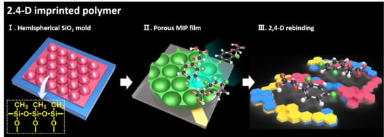
Figure 1.
Molecular imprinted polymer (MIP) formation via photosynthetic reaction using a functional template, monomer, crosslinker, and initiator for 2,4-D molecular imprinting sensors.
Figure 1.
Molecular imprinted polymer (MIP) formation via photosynthetic reaction using a functional template, monomer, crosslinker, and initiator for 2,4-D molecular imprinting sensors.

Figure 2.
(a) The systematic fabrication of the hemispherical silica replica, (b) scanning electron microscopy (SEM) (below is a cross-sectional image), and (c) atomic force microscopy (AFM) images of well-organized silica colloidal arrays with hexagonally ordered structures and the height profile presented. The scale bars are 1 μm.

Figure 3.
(a) Fabrication process of a porous MIP (st-MIP) film using a hemispherical silica replica as the master mold, (b) SEM (below is a cross-sectional image), and (c) AFM images (line profilometry is included below the AFM image) of the st-MIP film. The scale bars are 1 μm.
Figure 3.
(a) Fabrication process of a porous MIP (st-MIP) film using a hemispherical silica replica as the master mold, (b) SEM (below is a cross-sectional image), and (c) AFM images (line profilometry is included below the AFM image) of the st-MIP film. The scale bars are 1 μm.

Figure 4.
(a) Frequency change (Δf) on the n-MIP/NIP and st-MIP/NIP films as a function of time in a 100-nM 2,4-D aqueous solution for a 2-h rebinding process and (b) frequency change (Δf) as a function of 2,4-D’s concentration (from 40 to 100 nM).
Figure 4.
(a) Frequency change (Δf) on the n-MIP/NIP and st-MIP/NIP films as a function of time in a 100-nM 2,4-D aqueous solution for a 2-h rebinding process and (b) frequency change (Δf) as a function of 2,4-D’s concentration (from 40 to 100 nM).

Figure 5.
Expected molecular imprinting recognition on porous MIP films, obtained from surface imprinting using two replica molds: (a) st-replica mold and (b) n-replica mold.
Figure 5.
Expected molecular imprinting recognition on porous MIP films, obtained from surface imprinting using two replica molds: (a) st-replica mold and (b) n-replica mold.

Figure 6.
(a) Chemical structures of the three herbicide molecules and 2,4-D, and (b) the Δf values of the n- and st-MIP/NIP films in each of the analogous herbicide solution (2,4-D, atrazine, (4-chloro-2-methylphenoxy) acetic acid (MCPA), or ametryn) with a fixed concentration (100 nM) for a 2-h rebinding process.

Publisher’s Note: MDPI stays neutral with regard to jurisdictional claims in published maps and institutional affiliations. |
© 2021 by the authors. Licensee MDPI, Basel, Switzerland. This article is an open access article distributed under the terms and conditions of the Creative Commons Attribution (CC BY) license (http://creativecommons.org/licenses/by/4.0/).
Share and Cite
MDPI and ACS Style
Yang, J.C.; Hong, S.W.; Park, J. Improving Surface Imprinting Effect by Reducing Nonspecific Adsorption on Non-Imprinted Polymer Films for 2,4-D Herbicide Sensors. Chemosensors 2021, 9, 43. https://doi.org/10.3390/chemosensors9030043
AMA Style
Yang JC, Hong SW, Park J. Improving Surface Imprinting Effect by Reducing Nonspecific Adsorption on Non-Imprinted Polymer Films for 2,4-D Herbicide Sensors. Chemosensors. 2021; 9(3):43. https://doi.org/10.3390/chemosensors9030043
Chicago/Turabian StyleYang, Jin Chul, Suck Won Hong, and Jinyoung Park. 2021. "Improving Surface Imprinting Effect by Reducing Nonspecific Adsorption on Non-Imprinted Polymer Films for 2,4-D Herbicide Sensors" Chemosensors 9, no. 3: 43. https://doi.org/10.3390/chemosensors9030043
Note that from the first issue of 2016, this journal uses article numbers instead of page numbers. See further details here.