Article

Solution-Processed Functionalized MoS2 Nanosheets Composite for Photodetection Application

1
Institute for Nuclear Problems, Belarusian State University, 220006 Minsk, Belarus
2
Department of Materials Science, Institute of Optoelectronics, Fudan University, Shanghai 200437, China
3
A.N. Sevchenko Institute for Applied Physical Problems, Belarusian State University, 220006 Minsk, Belarus
4
B.I. Stepanov Institute of Physics, National Academy of Sciences of Belarus, 220072 Minsk, Belarus
5
Institute of Chemistry of New Materials, National Academy of Sciences of Belarus, 220072 Minsk, Belarus
*
Author to whom correspondence should be addressed.
These authors contributed equally to this work.
Photonics 2023, 10(12), 1295; https://doi.org/10.3390/photonics10121295
Submission received: 17 October 2023 / Revised: 11 November 2023 / Accepted: 22 November 2023 / Published: 24 November 2023
(This article belongs to the Special Issue Photodetector Materials and Optoelectronic Devices)

Abstract

:
Charge-transfer organic-inorganic complexes have demonstrated great potential in optoelectronic applications. Herein, a drop-casting processed photodetector based on thick composite films made of multi-layered MoS2 nanosheets chemically bonded to linear molecules of aromatic thiols has been developed. Composites based on multilayered nanosheets allow for facile preparation of low-cost, large-area, and flexible devices. It was demonstrated that a simple functionalization of ultradispersed MoS2 nanosheets with linear aromatic thiol results in the formation of charge and energy transfer complexes. A photodetector with functionalized MoS2 nanosheet film prepared by drop coating with Au electrodes demonstrated enhanced performance compared to pure materials. Our first experiments illustrated that functionalization of MoS2 nanosheets by a paraquaterphenyl thiol derivative leads to a significant increase in the photoresponse speed (by a factor of 12) and decay speed (by a factor of 17.5), in addition to the enhancement of the photostability of the MoS2 based photodetector. The photo current value has been increased by about an order of magnitude. The proposed approach offers promising prospects for further development of photodetectors.

1. Introduction

Photodetectors are essential for detecting and measuring light intensity using the function of converting optical signals to electrical signals. Photodetectors offer manifold various applications [1]. New materials and structures for photodetectors are constantly being developed due to the evolving applications and updated requirements. Two-D materials (such as graphene, transition metal dichalcogenides, etc.) have been ubiquitously used as the most promising semiconductor materials for this purpose [2,3]. Molybdenum disulfide (MoS2) nanosheets are among the most studied dichalcogenides [4,5]. This material has attracted more academic and applied interest due to its extraordinary properties arising from the internal structure of the nanosheets with d-electron interactions and its great degree of tunability. A single-layer MoS2 nanosheet forms a hexagonal lattice structure and contains three sublayers of atoms, where one layer of Mo atoms is sandwiched between two layers of S atoms. Most photodetector studies [6,7,8,9,10,11,12,13,14,15,16,17] use single-layered and multilayered individual nanosheets, though positive results with multilayered nanosheet composites in the sandwich structure were shown [18]. Single-layered nanosheets synthesized by CVD are widely known to be very time and energy-consuming and, therefore, expensive. Mechanically exfoliated nanosheets can be produced simply, but they have limitations in mass production. Multilayered MoS2 nanosheets for composite formation can be easily obtained by cheap, simple, and reliable liquid phase exfoliation [4]. Composites based on multilayered nanosheets can be solution-processed, which allows for facile preparation of low-cost, large-area, and flexible devices [19]. Unfortunately, the characteristics of these photodetectors are insufficiently high because of a lower ordering degree than the one in independent single nanosheets, as well as the presence of contacts between the nanosheets, resulting in lower conductivity. To achieve good performance of photodetectors (high responsibility, short response time, and high detectivity), both the physical and chemical functionalization of such nanosheets are widely utilized [3,13,14,15,16,17,20,21]. Many inorganic [1,3,12] and organic [3,8,9,13,14,15,16,17,20,21] nanomaterials have been used for functionalization. Most of the studies are devoted to physical functionalization [14,15,16,17,21]. However, chemical functionalization can provide more stable materials as it is irreversible. A wide variety of organic materials with different properties gives wide possibilities for functionalization. Promising results have been obtained with aliphatic thiols [11]. However, aromatic organic materials are electrically conductive and absorb light more strongly. Thus, in this study, we propose to apply the chemical functionalization of MoS2 multilayered nanosheets with a linear aromatic thiol, which is stable and luminescent. A combination of a n-type MoS2 nanosheet and a p-type aromatic molecule can form a charge transfer complex [22]. Often, high gain can be reached owing to the photogating effect [23,24], capable of achieving higher characteristics and escaping a cooling system, lowering the detector’s noise. Chemical functionalization of MoS2 nanosheets by organic molecules can be considered as covering by surfactant, which prevents nanosheets from aggregation [25], maintains stable interaction between nanosheets, and changes the properties of these nanosheets [26,27], which can be used for the creation of stable composite films. Thus, in this work, we propose to develop solution-processed films based on the newly synthesized material and study their photodetecting properties. Our approach results in the formation of a high-quality film, the enhancement of the photoresponse value and speed, and the photostability of the MoS2-based photodetector. Due to the simplicity of chemical functionalization, our proposed approach is promising for the further development of solution-processable photodetectors.

2. Materials and Methods

2.1. Materials

The MoS2 ultrafine powder with hexagonal lamellar structure was purchased from Graphene Supermarket (~90 nm average particle size, purity 99%, product number EM092222) and used as supplied. Functionalized MoS2 (MoS2-M) has been synthesized using this powder. Chlorobenzene (99.5%, CB) and isopropanol (99.8%) were used as received without further purification. MoS2 nanosheets were exfoliated in isopropanol based on a widely used exfoliation technique [4] with an ultrasonic tip for 12 h, resulting in the formation of a dispersion of MoS2 nanosheets with a wide range of sizes and thicknesses. After sonication, the dispersion has been used for optical measurements and film preparation.

2.2. MoS2 Nanosheets Functionalization

For the functionalization of the MoS2 nanosheets, 4-Hexyl-3′-methyl-4‴-mercapto-p-quaterphenyl (MQP) has been chosen. The chemical structure of MQP is presented in Figure 1.
The process of the chemical functionalization of MoS2 nanosheets with thiol molecules is simple and reliable, as presented in detail herein. Ultrasonic (US) disaggregation of the MoS2 ultrafine powder suspension in an organic solvent with the addition of MQP to maximize the MoS2 specific area and the MQP chemisorption has been applied. For this purpose, the following materials and apparatus were used: MoS2 ultrafine powder, DMF and n-hexane from Merck (Germany); MQP (synthesized); ultrasonic cleaner GT Sonic 1860QT (150 W, 40 kHz); centrifuge MDCEN-302-SD; diaphragm pump Wiggens C610; UV-lamp with 264 and 365 nm sources; glass round-bottom flasks.
A 50 mg MoS2 (MW 160 g/mol; 0.3 mmol) suspension in DMF (10 mL) was treated by US for 15 min in a round-bottom flask. After dispersion and continuing US treatment, a solution of 140 mg MQP (MW 436 g/mol; 0.3 mmol) in DMF (5 mL) was added with a rate of about one drop/s. Then, the reaction mixture was sonicated again for 1 h. The obtained suspension was evaporated and dried under vacuum (15 mm Hg, 50 °C, 30 min). The residue was dispersed in n-hexane (20 mL) under US to remove the excess MQP. This mixture was next separated in a centrifuge (6000 RPM, 5100 g, 30 min); the residue was rinsed with hexane (five times) until the solvent after centrifugation showed no fluorescence due to the traces of MQP when excited with a 365 nm UV light. After the purification, a wet material was dried on air at 50 °C.
MQP was synthesized specifically for this work, as it is not commercially available. The synthesis of MQP was carried out by the interaction of 4-hexyl-3′-methyl-4‴-Br-p-quaterphenyl (II) with n-butyllithium at a temperature ranging from −70 to −78 °C, followed by the addition of elemental sulfur. Next, 4-hexyl-3′-methyl-4‴-Br-p-quaterphenyl was obtained by the Suzuki reaction of 4-hexyl-3′-methyl-4‴-B(OH)2-p-terphenyl (I) with 4-bromoiodobenzene (see Scheme 1).
The 4-Hexyl-3′-methyl-4‴-bromo-p-quaterphenyl (II) (4,83 g, 10 mmol) was dissolved in 50 mL of dry THF, and the solution was cooled in an argon atmosphere to −80–70 °C with continuous stirring. At this temperature, an n-butyllithium solution (5 mL of 2.5M solution in hexane) was added by syringe, and the reaction mixture was stirred for 1 h at the same temperature. The sulfur solution (0.384 g, 12 mmol) in 30 mL THF was added to this mixture by syringe. The mixture was gradually allowed to warm up to 20 °C, followed by the addition of 50 mL of 2% hydrochloric acid. The organic layer was separated, and the aqueous layer was extracted with two 30 mL portions of toluene. The combined organic layer was washed with water twice and dried over the anhydrous magnesium sulfate. After filtration, the solvent was removed in a vacuum to yield 4.22 g of crude 4-hexyl-3′-methyl-4‴-mercapto-p-quaterphenyl. The crude product was recrystallized from the acetonitrile/acetone (3/1) solution. The yield of MQP was 3.76 g (86%). The 1H NMR (400 MHz, CDCl3, δ, ppm) was 7.85 (m, 1 H), 7.73~7.63 (m, 5 H), 7.25~7.45 (m, 10 H), 7.06 (m, 1 H), 3,40 SH, 2.77~2.62 (m, 2 H), 2.59 (s,3 H), 1.59 (dd, J = 14.6, 7.0 Hz, 2 H), 1.29 (dd, J = 8.6, 5.3 Hz, 4 H), and 0.91 (t, J = 6.6 Hz, 3 H).
Compound II has been synthesized following the procedure described below. The mixture of 4-bromoiodobezene 4.53 g (16 mmol), 4-hexyl-3′-methyl-p-terphenyl-4‴-boronic acid (I) 4.67 g (12,5 mmol), potassium carbonate 4.2 g (30 mmol), acetone (60 mL), THF (20 mL), and water (40 mL) was refluxed upon continuous stirring for 0.5 h in an argon atmosphere, followed by the addition of palladium acetate (20 mg). The reaction mixture was refluxed under stirring for 3 h. Upon the evaporation of acetone, 1N solution hydrochloric acid was added at pH = 2. The crude product was extracted with methylene chloride, washed with water, and dried over anhydrous magnesium sulfate (MgSO4). The crude product was then purified by column chromatography (using silica gel, methylene chloride as eluent). The solvent was removed using a rotary evaporator, and the product was recrystallized from acetonitrile/acetone (3/1). The yield of II was 5.41 g (89%): 1H NMR (400 MHz, CDCl3, δ, ppm): 7.85 (m, 1 H), 7.73~7.66 (m, 5 H), 7.25~7.45 (m, 10 H), 7.06 (m, 1 H), 2.77~2.62 (m, 2 H), 2.59 (s,3 H), 1.59 (dd, J = 14.6, 7.0 Hz, 2 H), 1.29 (dd, J = 8.6, 5.3 Hz, 4 H), 0.91 (t, J = 6.6 Hz, 3 H); MS(ESI): 484,482 (M+), 413,411.
The synthesis of 4-hexyl-3′-methyl-4‴-B(OH)2-p-terphenyl (I) was carried out following the procedure described in the literature [28].
MoS2 nanosheets can be presented by several polymorphs, depending on the interlayer stacking arrangement and intralayer coordination between the central Mo atom and the surrounding S atoms [3,4,5]. The exact nature of organic thiol and exfoliated MoS2 interactions remains unclear [29]. Thus, it is not clear where the thiol group of the molecule can be bonded to the MoS2 nanosheet. Typically, the defect-free area of a MoS2 basal plane is inert. However, it was observed that an S atom of thiol can be attached to the Mo [30,31] or S [30,32,33] atoms at vacancy defects. Mo atoms can be reached at the edges of the nanosheet, while S atoms can be accessible at the basal planes.

2.3. Thin Film Preparation

Thin films were obtained by drop-casting the obtained suspension on the substrate or by spin-coating. For thin film deposition, we used either 0.5 mm thick quartz substrates transparent for wavelengths above 200 nm or silicon surface for device preparation. All substrates were carefully cleaned with acetone and ethanol and were dried before thin-film deposition.

2.4. Device Fabrication

First, the sample powder was added to the CB solvent and sonicated for 12 h to form a dispersion. After that, uniform films were cast on a clean SiO2/Si substrate by drop/spin coating, followed by annealing at a specific temperature for 1 h. To ensure the cleanliness of the substrate, it is necessary to perform ultrasonic cleaning treatment on the substrates before usage. Specifically, the SiO2/Si substrates are cleaned with acetone and isopropyl alcohol and deionized water for 30 min. Acetone and alcohol can remove the majority of organic impurities from the substrates’ surface, and deionized water can wash away the remaining particle contaminants. To improve film homogeneity, the samples need to be annealed. However, because regular annealing temperatures for inorganic materials [34] are too high for organic materials, we lowered the annealing temperature and shortened the annealing time for composite samples to 80 °C for 1 h. Unfortunately, such a low temperature cannot remove all defects. The thickness of the active layer film for both devices is about 1.3 µm (1.32 µm for MoS2 and 1.28 µm for MoS2-M). After optimizing synthesis parameters and obtaining uniform, high-quality films, Au electrodes (70 nm thick) were plated on the film by thermal vacuum evaporation. As a result, two kinds of photodetectors (PDs) based on pure MoS2 and doped MoS2 were formed.

2.5. Characterization

Systematic characterizations were carried out to determine the properties of functionalized MoS2 nanosheets and their individual counterparts.
Absorption spectra were recorded with a Cary 500 (Varian, Palo Alto, CA, USA) spectrophotometer. Photoluminescence and excitation spectra were measured with a multifunctional spectral fluorimeter, Fluorolog-3 (Horiba Scientific, Palaiseau, France), which provides highly sensitive and stable measurements in the ultra-violet and visible range. All photoluminescence measurements for solutions were made perpendicularly to the excitation beam, and thin films were oriented at 30°. Raman spectra have been obtained at room temperature with a micro-Raman spectrometer Nanofinder High End (Lotis TII, Minsk, Belarus—Tokio Instruments, Tokio, Japan; 1800 lines/mm grating; 50× objective; 532 nm excitation wavelength). The morphology of the dispersed phase was examined using a field emission scanning electron microscope (FESEM), Zeiss Sigma, and scanning electron microscope MIRA3 (Tescan, Brno, Chech Republic). The thickness of the film is determined by a step profilometer (KLA-Tencor, Milpitas, CA, USA). All measurements were carried out at room temperature and ambient conditions. The molecular structure of the synthesized organic compounds was verified using 1H NMR spectra acquired on a Bruker AVANCE 500 spectrometer at room temperature and mass spectra acquired on an Agilent 6410 Triple Quadrupole LC/MS System.
Optoelectronic properties were collected using the semiconductor characterization system Keithley 4200-SCS (Tektronix, Beaverton, OR, USA) connected to a vacuum probe station (Lake Shore). A 75 W Xe lamp equipped with a monochromator was used as a light source. Light density was measured by a NOVA II power meter (OPHIR photonics, Jerusalem, Israel). All the measurements were performed at ambient environment, i.e., room temperature and atmospheric pressure.

3. Results and Discussion
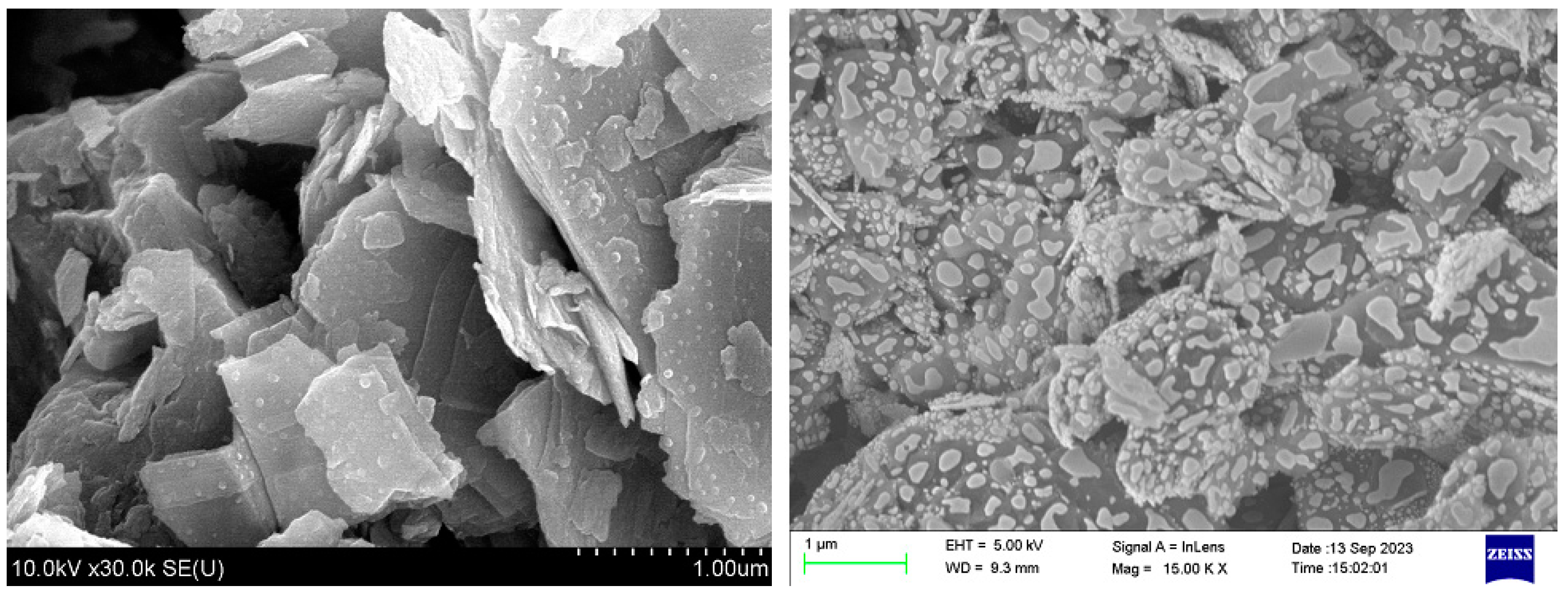
3.1. Microscopy

Electron microscopy provides insights into the morphology of the films. Figure 2 represents an SEM picture of the morphology of MoS2 and MoS2−M films. It can be seen that this sample consists of large nanosheets (of several micrometers) covered with small particles, hinting that US treatment was not complete, especially for pure MoS2. Dispersion size and concentration are known to depend on sonication time and power [35]. The plane of the large nanosheets is located mainly parallel to the plane of the substrate surface, and the small nanosheets are positioned similarly on the surface of the large nanosheets (see Figure 2, right). Additionally, no fundamental difference between MoS2 and MoS2-M film morphology has been observed. Hence, only a small part of the nanosheet surface has been covered with molecules that are typically oriented perpendicularly to its surface. The combination of large and small particles can result in higher conductivity owing to the denser packing of the particles. Note that the low-resolution microscopy reveals a much lower quality of the pure MoS2 nanosheet film than the film made of MoS2-M nanosheets. MoS2 film samples contain numerous inhomogeneities and hollow cavities. Functionalized MoS2 nanosheet films are much more homogeneous than nonfunctionalized material because of better interaction between the nanosheets caused by thiol molecules.

3.2. Raman Spectra

Raman spectroscopy is known to be a reliable diagnostic tool for studying the thickness of MoS2 nanosheets, as well as various interactions [36]. Raman spectra of unsonicated MoS2 and functionalized MoS2−M samples (Figure 3) excited with a 532 nm laser were obtained. Both spectra contain two main modes of out-of-plane vibrations (A1g) of S atoms and in-plane vibrations (E12g) of Mo atoms and S atoms. The original MoS2 nanosheets show these peaks at about 381 and 407 cm−1, with the difference between them of ~26 cm−1 implying that this sample contains nanosheets with thicknesses ranging from monolayer to, preferably, several layers. Functionalized MoS2 nanosheets show a negligible (about 1 cm−1) redshift of both peaks with the same peak intensity ratio but a noticeable broadening of both peaks. These data confirm the presence of both S−S and S−Mo bonds owing to the successful MoS2 functionalization. Note that the measurements were made at five points with different nanosheet dimensions, distribution, and morphology for both samples. It was shown that the only observed difference was the signal intensity.

3.3. Absorption and Luminescence

Optical absorption and luminescence spectra can give information about the position of energy levels and energy transformation in the considered system. Figure 4 illustrates the normalized absorption, excitation, and luminescence spectra of MoS2−M and the corresponding components (MoS2 and MQP). The absorption spectrum of MoS2−M is approximately a superposition of the absorption of both individual components. However, a longwave shoulder at about 350 nm can be considered a charge transfer band. Indeed, the relative intensity of this shoulder is much higher than that of the MoS2 spectrum, though the deposition of MQP is negligible. Partial overlapping of MoS2 absorption and MQP luminescence spectra can result in the partial energy transfer from MQP to MoS2. Blue luminescence of MoS2 occurs, probably, from higher energy levels as described in [37,38,39,40]. It is weak compared to the luminescence of MQP and the composite. No red luminescence is observed in the system of few-layered MoS2 nanosheets. The luminescence spectrum of the hybrid sample is red-shifted by about 19 nm and broadened compared to the MQP spectrum because of the partial superposition of the luminescence spectra of both counterparts. The intensity of its luminescence is much weaker than that of MQP. This finding indicates that a charge transfer from MQP to MoS2 occurs, which is confirmed by the almost fully coinciding excitation spectra of MQP and MoS2-M. Thus, in this system, both energy and charge transfer can be observed.

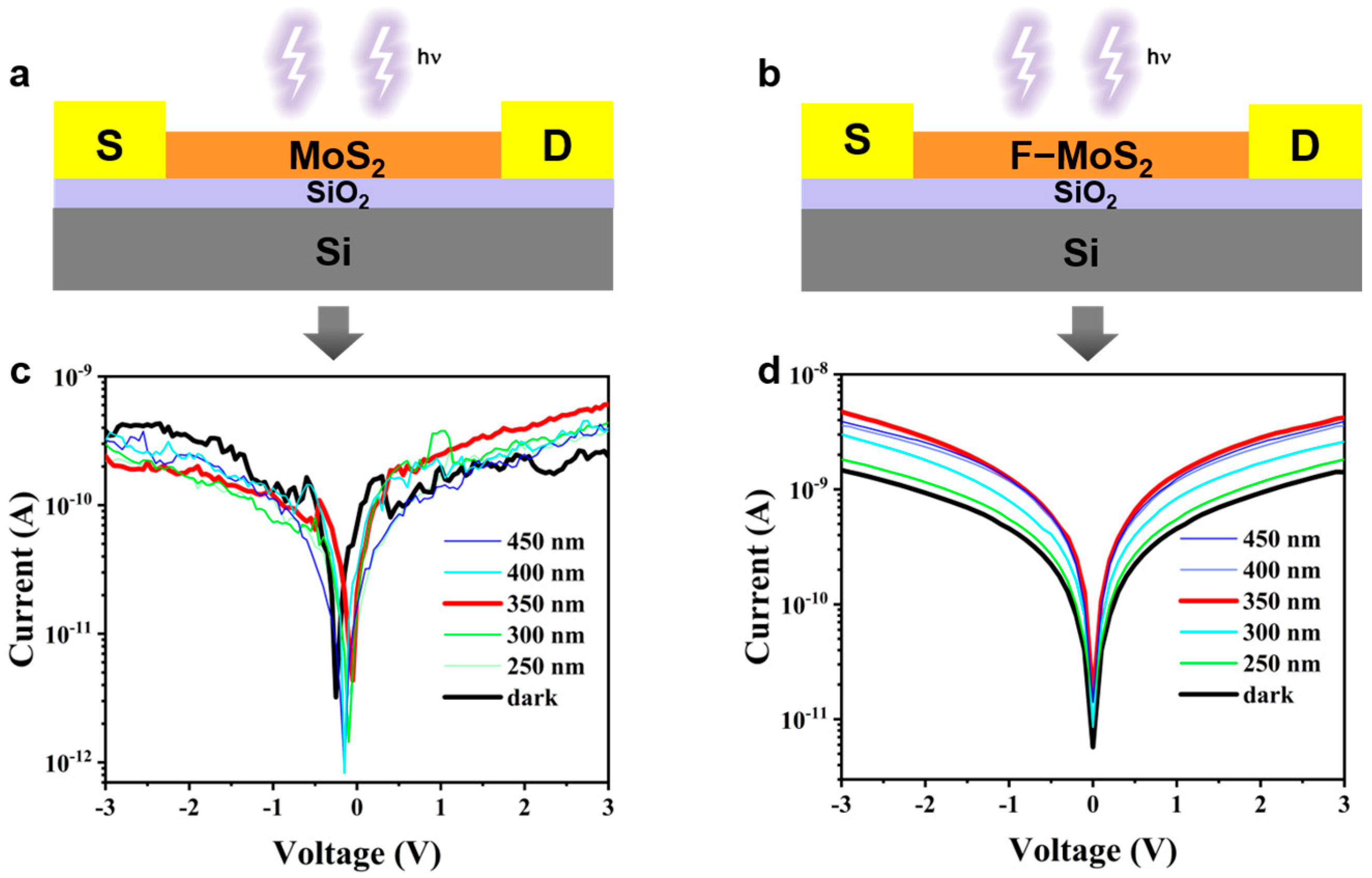
3.4. Current-Voltage Characteristics of Photodetectors

Subsequently, the optoelectronic performance of the constructed devices was tested. The length of the devices’ channel is 100 μm, and the width of the gold electrodes is 500 μm. The thickness of SiO2 is 300 nm, which is sufficient to eliminate the interference of the bottom substrate (silicon) signal. As seen from Figure 5a,b, the structures of the devices based on pure MoS2 and MoS2−M are similar, with the only difference in the composition of the photosensitive layer with the same thickness of about 1.3 μm. As a result, as shown in Figure 5c,d representing I-V test results, there are two obvious improvements in optoelectronic performance after the doping of organic molecules. On the one hand, both dark and photocurrent were increased by about one order of magnitude. On the other hand, the current signals are much more stable than that of pure MoS2. Compared to the pure MoS2 device, the organic molecules−doped MoS2 device shows significant positive effects. Before doping, the fabricated device shows obvious current instability, both dark current and photocurrent, indicating that the charge carrier transmission is very inefficient. This may be caused by the high defect density of materials, low carrier mobility, small diffusion length, etc. More importantly, the film quality of pure MoS2 is limited without the MoS2 doping, which will affect the generation, separation, transportation, and recombination of photogenerated carriers to a great degree, thus leading to poor performance with jittering intense current signals and slow response behavior under light illumination. It should be noted that the dark current at negative bias is higher than the photocurrent at different wavelengths of laser irradiation, indicating that the photodetectors do not have any photo gain at negative bias. In contrast, positive bias does not have this problem. The reason for this phenomenon can be the formation of Schottky contacts between metal and semiconductors. In the case of Schottky contact, the band of semiconductor at the interface is curved, thus forming a Schottky barrier and showing a nonlinear I-V behavior under positive/negative bias. It is, therefore, rational that the photocurrent is higher than the dark current at positive bias and lower at negative bias because of the existence of a built-in electric field. This property can be changed with Ohmic contacts in the case of corresponding energy levels of electrode and semiconductor. On the other side, gold electrodes can be replaced by polymer electrodes.

3.5. Photoresponse Kinetics

To further study the enhancement of the optoelectronic performance of doped−MoS2-based photodetectors, we performed time-dependent I-t tests of the devices. The incident laser power over the fabricated device is 228 μW cm−2 (at 350 nm). As seen in Figure 6b, compared to pure MoS2, the MoS2−M−based PD exhibits better properties with higher currents and more stable photocurrents, especially with faster response speed. As specifically shown in Figure 6c,d, the rise τrise and decay τdecay time of pure MoS2 are 5.2 s and 14.8 s, respectively, and the τrise and τdecay time of MoS2−M are 0.4 s and 0.8 s, respectively, which means the response speed is increased by 12 times, and the decay speed is increased by 17.5 times. These rise and decay times originate because of the presence of nanosheet edges acting as traps [17] retarding the movement of charges. Note that there are fast and slow decay components (Figure 6). This tail of the slow decay component can be attributed to the adsorption of molecules of oxygen and water from air [15] and other long-lived traps.
Interestingly, the response speed and photocurrent stability were greatly improved. We attribute these improvements to the good electrical conductivity of organic molecules, which creates better contacts and connections between the nanosheets. This result improves film quality with better morphology, such as better particle distribution, improved uniformity, more substantial filling, etc., that is in consistent with the microscopy data. This factor facilitates the transport of photo-generated carriers and improves charge carrier dynamics and photocurrent stability. Indeed, better contacts between nanosheets in functionalized samples increase the flow of charges as occurs in graphene nanosheets with metal nanoparticles fully covered by aromatic thiol molecules [41], which can be noticed as the increase in response speed and value. Also, light absorption is increased after the MoS2 functionalization due to the additional absorption by the organic molecules. It can be concluded from the above results that doping by organic molecules enhances the photoresponse speed and the photostability of MoS2. Although the device performance is not outstanding compared to the device based on the mechanically exfoliated MoS2, this novel doping strategy of combining organic molecules with transition metal dichalcogenides can result in the realization of stable and accurate control of photo-generated carriers in a composite film. It has great significance for expanding the application potential of two-dimensional materials in semiconductor optoelectronic devices.

4. Conclusions

The photodetector based on thick composite films made of multi-layered MoS2 nanosheets chemically bonded with linear molecules of aromatic thiols has been developed. Composites based on multilayered nanosheets can be solution-processed, which allows for the simple fabrication of low-cost, large-area, and flexible devices. The sample consists of large nanosheets (of several micrometers) covered with small MoS2 particles. Raman line-broadening and red-shift to lower-wavenumbers of the MoS2 peaks confirm the formation of the functionalized composite. Both absorption and luminescence spectra are the superposition of the corresponding components. However, the long-wavelength shoulder at about 350 nm in the absorption spectrum of the composite can be considered as a charge transfer band. It was found that the functionalization of MoS2 nanosheets with a paraquaterphenyl thiol derivative greatly enhances the photoresponse value, speed, and photostability of MoS2-based photodetector. This study represents our first steps in the proposed direction and requires further experiments. The proposed approach is very promising for further development, for example, the use of higher dispersity, choice of a functionalizing molecule, and degree and type of functionalization.

Author Contributions

Conceptualization, A.V.K. and X.F.; methodology, A.V.K. and A.L.; software, N.B.; validation, I.N.K.; formal analysis, I.N.K.; investigation, E.H. and N.B.; resources, U.P. and A.L.; data curation, A.L. and T.A.P.; writing—original draft preparation, A.V.K. and E.H.; writing—review and editing, A.V.K.; visualization, N.I.V.; supervision, S.A.M. and X.F.; project administration, Z.L.; funding acquisition, S.A.M. and X.F. All authors have read and agreed to the published version of the manuscript.

Funding

The authors extend their appreciation to the Belarusian Foundation for Fundamental Research (Project No T23KI-004) for funding and supporting this work. Xiaosheng Fang acknowledges the support from National Natural Science Foundation of China (No. 12211530438) and the Office of Global Partnerships (Key Projects Development Fund).

Institutional Review Board Statement

Not applicable.

Informed Consent Statement

Not applicable.

Data Availability Statement

The data that support the findings of this study are available within the article.

Acknowledgments

The authors extend their appreciation to the Belarusian Foundation for Fundamental Research for funding and supporting this work. Xiaosheng Fang acknowledges the support from the National Natural Science Foundation of China and the Office of Global Partnerships (Key Projects Development Fund).

Conflicts of Interest

The authors declare no conflict of interest.

References

  1. Li, Z.Q.; Yan, T.T.; Fang, X.S. Low-dimensional wide-bandgap semiconductors for UV photodetectors. Nat. Nanotech. Nat. Rev. Mater. 2023, 8, 587–603. [Google Scholar] [CrossRef]
  2. Cheng, J.; Wang, C.; Zou, X.; Liao, L. Recent advances in optoelectronic devices based on 2D materials and their heterostructures. Adv. Opt. Mater. 2019, 7, 1800441. [Google Scholar] [CrossRef]
  3. Malik, M.; Iqbal, M.A.; Choi, J.R.; Pham, P.V. 2D materials for efficient photodetection: Overview, mechanisms, performance and UV-IR range applications. Front. Chem. 2022, 10, 905404. [Google Scholar] [CrossRef]
  4. Samy, O.; Zeng, S.; Birowosuto, M.D.; El Moutaouakil, A. A review on MoS2 properties, synthesis, sensing applications, and challenges. Crystals 2021, 11, 355. [Google Scholar] [CrossRef]
  5. Nalwa, H.S. A review of molybdenum disulfide (MoS2) based photodetectors: From ultra-broadband, selfpowered to flexible devices. RSC Adv. 2020, 10, 30529–30602. [Google Scholar] [CrossRef] [PubMed]
  6. Yu, F.; Hu, M.; Kang, F.; Lv, R. Flexible photodetector based on large-area few-layer MoS2. Progress. Nat. Sci. Mater. Int. 2018, 28, 563–568. [Google Scholar] [CrossRef]
  7. Liu, X.; Hu, S.; Lin, Z.; Li, X.; Song, L.; Yu, W.; Wang, Q.; He, W. High-performance MoS2 photodetectors using a patterned gallium nitride substrate. ACS Appl. Mater. Interfaces 2021, 13, 15820–15826. [Google Scholar] [CrossRef] [PubMed]
  8. Mutz, N.; Park, S.; Schultz, T.; Sadofev, S.; Dalgleish, S.; Reissig, L.; Koch, N.; List-Kratochvil, E.J.W.; Blumstengel, S. Excited-state charge transfer enabling MoS2/phthalocyanine photodetectors with extended spectral sensitivity. J. Phys. Chem. C 2020, 124, 2837–2843. [Google Scholar] [CrossRef]
  9. Kiriya, D.; Tosun, M.; Zhao, P.; Kang, J.S.; Javey, A. Air-stable surface charge transfer doping of MoS2 by benzyl viologen. J. Am. Chem. Soc. 2014, 136, 7853–7856. [Google Scholar] [CrossRef] [PubMed]
  10. Nur, R.; Tsuchiya, T.; Toprasertpong, K.; Terabe, K.; Takagi, S.; Takenaka, M. High responsivity in MoS2 phototransistors based on charge trapping HfO2 dielectrics. Communs. Mat. 2020, 1, 103. [Google Scholar] [CrossRef]
  11. Wu, S.; Wu, G.; Wang, X.; Chen, Y.; Lin, T.; Shen, H.; Hu, W.; Meng, X.; Wang, J.; Chu, J. A gate-free MoS2 phototransistor assisted by ferroelectrics. J. Semicond. 2019, 40, 092002. [Google Scholar] [CrossRef]
  12. Tsai, T.-H.; Liang, Z.-Y.; Lin, Y.-C.; Wang, C.-C.; Lin, K.-I.; Suenaga, K.; Chiu, P.-W. Photogating WS2 photodetectors using embedded WSe2 charge puddles. ACS Nano. 2020, 14, 4559–4566. [Google Scholar] [CrossRef] [PubMed]
  13. Huang, Y.; Zhuge, F.; Hou, J.; Lv, L.; Luo, P.; Zhou, N.; Gan, L.; Zhai, Z. Van der Waals coupled organic molecules with monolayer MoS2 for fast response photodetectors with gate-tunable responsivity. ACS Nano. 2018, 12, 4062–4073. [Google Scholar] [CrossRef] [PubMed]
  14. Raoufi, M.; Rühl, S.; Chandrabose, S.; Shukla, A.; Sun, B.; Kratochvil, E.-L.; Blumstengel, S.; Neher, D. Fast Photoresponse from hybrid monolayer MoS2/organic photodetector. Phys. Status Solidi A 2023, 2300107. [Google Scholar] [CrossRef]
  15. Di Bartolomeo, A.; Kumar, A.; Durante, O.; Sessa, A.; Faella, E.; Viscardi, L.; Intonti, K.; Giubileo, F.; Martucciello, N.; Romano, P.; et al. Temperature-dependent photoconductivity in two-dimensional MoS2 transistors. Mater. Today Nano. 2023, 24, 100382. [Google Scholar] [CrossRef]
  16. Andleeb, S.; Wang, X.; Dong, H.; Valligatla, S.; Saggau, C.N.; Ma, L.; Schmidt, O.G.; Zhu, F. Fast-response micro-phototransistor based on MoS2/organic molecule heterojunction. Nanomaterials 2023, 13, 1491. [Google Scholar] [CrossRef] [PubMed]
  17. Xu, Z.H.; He, M.; Wu, Q.; Wu, C.C.; Li, X.B.; Liu, B.L.; Tang, M.-C.; Yao, J.; Wei, G. Ultrafast charge transfer 2D MoS2/organic heterojunction for sensitive photodetector. Adv. Sci. 2023, 10, 2207743. [Google Scholar] [CrossRef]
  18. Cunningham, G.; Khan, U.; Backes, C.; Hanlon, D.; McCloskey, D.; Donegan, J.; Coleman, J.N. Photoconductivity of solution-processed MoS2 films. J. Mater. Chem. C 2013, 1, 6899–6904. [Google Scholar] [CrossRef]
  19. Hu, Y.; Li, Z.Q.; Fang, X.S. Solution-prepared AgBi2I7 Thin Films and Their Photodetecting Properties. J. Inorg. Mater. 2023, 38, 1055–1061. [Google Scholar] [CrossRef]
  20. Daukiya, L.; Seibel, J.; De Feyter, S. Chemical modification of 2D materials using molecules and assemblies of molecules. Adv. Phys. X 2019, 4, 1625723. [Google Scholar] [CrossRef]
  21. Molina-Mendoza, A.J.; Vaquero-Garzon, L.; Leret, S.; de Juan-Fernández, L.; Pérez, E.M.; Castellanos-Gomez, A. Engineering the optoelectronic properties of MoS2 photodetectors through reversible noncovalent functionalization. Chem. Communs. 2016, 52, 14365–14368. [Google Scholar] [CrossRef] [PubMed]
  22. Tajima, T.; Okabe, S.; Takaguchi, Y. Photoinduced electron transfer in a MoS2/anthracene mixed-dimensional heterojunction in aqueous media. Bull. Chem. Soc. Jpn. 2020, 93, 745–750. [Google Scholar] [CrossRef]
  23. Fang, H.; Hu, W. Photogating in low dimensional photodetectors. Adv. Sci. 2017, 4, 1700323. [Google Scholar] [CrossRef]
  24. Shin, J.; Yoo, H. Photogating effect-driven photodetectors and their emerging applications. Nanomaterials 2023, 13, 882. [Google Scholar] [CrossRef]
  25. Smith, R.J.; King, P.J.; Lotya, M.; Wirtz, C.; Khan, U.; De, S.; O’Neill, A.; Duesberg, G.S.; Grunlan, J.C.; Moriarty, G.; et al. Large-scale exfoliation of inorganic layered compounds in aqueous surfactant solutions. Adv. Mater. 2011, 23, 3944–3948. [Google Scholar] [CrossRef]
  26. Palenzuela, C.L.M.; Luxa, J.; Sofer, Z.; Pumera, M. MoSe2 dispersed in stabilizing surfactant media: Effect of the surfactant type and concentration on electron transfer and catalytic properties. ACS Appl. Mater. Interfaces 2018, 10, 17820–17826. [Google Scholar] [CrossRef] [PubMed]
  27. Shyyko, L.O.; Kotsyubynsky, V.O.; Budzulyak, I.M. The importance of surfactant and its type on MoS2 nanoparticles formation. J. Nanosci. Nanotech. 2016, 16, 7792–7796. [Google Scholar] [CrossRef]
  28. Sasnouski, G.; Lapanik, V.; Bezborodov, V.; Dabrowski, R.; Dziaduczek, J. Synthesis of fluoro substituted quaterphenyl liquid crystals. Phase Transit. 2014, 87, 783–789. [Google Scholar] [CrossRef]
  29. Chen, X.; McGlynn, C.; McDonald, A.R. Two-dimensional MoS2 catalyzed oxidation of organic thiols. Chem. Mater. 2018, 30, 6978–6982. [Google Scholar] [CrossRef]
  30. Makarova, M.; Okawa, Y.; Aono, M. Selective adsorption of thiol molecules at sulfur vacancies on MoS2(0001), followed by vacancy repair via S−C dissociation. J. Phys. Chem. C 2012, 116, 22411–22416. [Google Scholar] [CrossRef]
  31. Canton-Vitoria, R.; Sayed-Ahmad-Baraza, Y.; Pelaez-Fernandez, M.; Arenal, R.; Bittencourt, C.; Ewels, C.P.; Tagmatarchis, N. Functionalization of MoS2 with 1,2-dithiolanes: Toward donoracceptor nanohybrids for energy conversion. Npj 2D Mater. Appl. 2017, 1, 13. [Google Scholar] [CrossRef]
  32. Chen, X.; Denninger, P.; Stimpel-Lindner, T.; Spiecker, E.; Duesberg, G.S.; Backes, C.; Knirsch, K.C.; Hirsch, A. Defect engineering of two-dimensional molybdenum disulfide. Chem. Eur. J. 2020, 26, 6535–6544. [Google Scholar] [CrossRef] [PubMed]
  33. Gul, A.; Bacaksiz, C.; Unsal, E.; Akbali, B.; Tomak, A.; Zareie, H.M.; Sahin, H. Theoretical and experimental investigation of conjugation of 1,6- hexanedithiol on MoS2. Mater. Res. Express. 2018, 5, 036415. [Google Scholar] [CrossRef]
  34. Wu, S.Q.; Wang, X.D.; Jiang, W.; Tu, L.; Chen, Y.; Liu, J.; Lin, T.; Shen, H.; Ge, J.; Hu, W.; et al. Interface engineering of ferroelectric-gated MoS2 phototransistor. Sci. China Inf. Sci. 2021, 64, 140407. [Google Scholar] [CrossRef]
  35. O’Neill, A.; Khan, U.; Coleman, J.N. Preparation of high concentration dispersions of exfoliated MoS2 with increased flake size. Chem. Mater. 2012, 24, 2414–2421. [Google Scholar] [CrossRef]
  36. Yang, P.; Zhang, Z.; Sun, M.; Lin, F.; Cheng, T.; Shi, J.; Xie, C.; Shi, Y.; Jiang, S.; Huan, Y.; et al. Thickness tunable wedding-cake-like MoS2 flakes for high-performance optoelectronics. ACS Nano 2019, 26, 3649–3658. [Google Scholar] [CrossRef]
  37. Ha, H.D.; Han, D.J.; Choi, J.S.; Park, M.; Seo, T.S. Dual role of blue luminescent MoS2 quantum dots in fluorescence resonance energy transfer phenomenon. Small 2014, 10, 3858–3862. [Google Scholar] [CrossRef]
  38. Park, S.J.; Pak, S.W.; Qiu, D.; Kang, J.H.; Song, D.Y.; Kim, E.K. Structural and optical characterization of MoS2 quantum dots defined by thermal annealing. J. Lum. 2017, 183, 62–67. [Google Scholar] [CrossRef]
  39. Feng, S.; Lv, J.; Pei, F.; Lv, X.; Wu, Y.; Hao, Q.; Zhang, Y.; Tong, Z.; Lei, W. Fluorescent MoS2 QDs based on IFE for turn-off determination of FOX-7 in real water samples. Spectrochim. Acta A Mol. Biomol. Spectrosc. 2020, 231, 118131. [Google Scholar] [CrossRef]
  40. Manamel, L.T.; Mukherjee, A.; Das, B.C. Two-dimensional nanohybrid of MoS2 and Rose Bengal: Facile solution growth and band structure probing. Appl. Surf. Sci. 2020, 530, 147063. [Google Scholar] [CrossRef]
  41. Kukhta, A.V.; Paddubskaya, A.G.; Kuzhir, P.P.; Maksimenko, S.A.; Vorobyova, S.A.; Bistarelli, S.; Cataldo, A.; Belucchi, S. Copper nanoparticles decorated graphene nanoplatelets and their polymer composites. Synth. Met. 2016, 222, 192–197. [Google Scholar] [CrossRef]
Figure 1. Chemical structure of MQP molecule.
Photonics 10 01295 g001
Scheme 1. Synthetic route 4-hexyl-3′-methyl-4‴-mercapto-p-quaterphenyl (MQP).
Photonics 10 01295 sch001
Figure 2. FESEM scans of the MoS2 (left) and the MoS2−M (right) thin film samples.
Photonics 10 01295 g002
Figure 3. Normalized Raman spectra of MoS2−M (solid) and MoS2 (dashed) thin films.
Photonics 10 01295 g003
Figure 4. Normalized absorption (1,4,7), luminescence (2,5,8), and luminescence excitation (3,6) spectra of MoS2−M (1–3), MQP (4–6), and MoS2 (7,8) isopropanol solutions.
Photonics 10 01295 g004
Figure 5. (a,b) The device structures of pure MoS2−based and MoS2−M−based PDs; (c) I–V curves of pure MoS2−based PD; and (d) I–V curves of doped−MoS2−based PD.
Photonics 10 01295 g005
Figure 6. (a) Schematic illustration of the device architecture (i) and an optical microscope image of the real device (ii); (b) photoresponse comparison of pure MoS2−based and MoS2−M−based PDs; (c) semilogarithmic I-t curves of pure MoS2−based PD under 350 nm illumination on/off switching at 3 V; (d) semilogarithmic I-t curves of MoS2−M−based PD under 350 nm illumination on/off switching at 3 V.
Photonics 10 01295 g006
Disclaimer/Publisher’s Note: The statements, opinions and data contained in all publications are solely those of the individual author(s) and contributor(s) and not of MDPI and/or the editor(s). MDPI and/or the editor(s) disclaim responsibility for any injury to people or property resulting from any ideas, methods, instructions or products referred to in the content.

