Quantum Dot Lasers Directly Grown on 300 mm Si Wafers: Planar and In-Pocket
by
 , , ,
, , ,
Kaiyin Feng
1 ,
,
Chen Shang
2,
Eamonn Hughes
2,
Andrew Clark
3,
Rosalyn Koscica
2,
Peter Ludewig
4,
David Harame
5 and
John Bowers
1,2,*
1
Department of Electrical and Computer Engineering, University of California Santa Barbara, Santa Barbara, CA 93106, USA
2
Materials Department, University of California Santa Barbara, Santa Barbara, CA 93106, USA
3
IQE, Inc., Greensboro, NC 27409, USA
4
NAsPIII–V GmbH, 35032 Marburg, Germany
5
RF SUNY Polytechnic Institute, Albany, NY 12203, USA
*
Author to whom correspondence should be addressed.
Photonics 2023, 10(5), 534; https://doi.org/10.3390/photonics10050534
Submission received: 29 March 2023
/
Revised: 30 April 2023
/
Accepted: 2 May 2023
/
Published: 6 May 2023
(This article belongs to the Special Issue Nanophotonics Pioneer: Prof. Dr. Dieter Bimberg ‘Green Photonics Networks: From VCSELs to Nanophotonics’)
Abstract
:We report for the first time the direct growth of quantum dot (QD) lasers with electrical pumping on 300 mm Si wafers on both a planar template and in-pocket template for in-plane photonic integration. O-band lasers with five QD layers were grown with molecular beam epitaxy (MBE) in a 300 mm reactor and then fabricated into standard Fabry–Perot ridge waveguide cavities. Edge-emitting lasers are demonstrated with high yield and reliable results ready for commercialization and scaled production, and efforts to make monolithically integrated lasing cavities grown on silicon-on-insulator (SOI) wafers vertically aligned and coupled to SiN waveguides on the same chip show the potential for 300 mm-scale Si photonic integration with in-pocket direct MBE growth.
1. Introduction
There has been rapid progress in scaling the production of Si photonic integrated circuits (PICs) in the past decades as energy-efficient, high-performance, on-chip photonic systems for various applications, such as optical interconnects, light detection and ranging (LiDAR) technology, and quantum communications [1,2,3,4,5,6,7]. Leveraging the advantages of using integrated fabrication process resembling complementary metal-oxide semiconductor (CMOS) technology in integrated circuits, the recent development of Si photonic foundry platforms has enabled a large wafer scale, low production cost, and the high yield manufacturing of active and passive photonic components [2,8,9,10]. For example, multi-project wafer (MPW) services assembled on silicon-on-insulator (SOI) platforms are offered with up to 300 mm wafer size with fast turnaround time and stable device performance [11]. When it comes to light source integration on Si, the challenges of incorporating III-V-based gain media such as GaAs or InP have brought limitations to PIC production scalability and yield, and the dominant choices remain off-chip co-packaging and heterogeneous integration [12,13,14,15,16,17].
The monolithic integration of III-V light sources on Si through heteroepitaxial growth with molecular-beam epitaxy (MBE) and metalorganic chemical vapor deposition (MOCVD) has gained major attention in recent years [18,19,20,21,22,23,24], highlighting the merits of using quantum dots (QDs) as the gain material [25,26,27,28], especially with their improved tolerance to crystalline defects [29,30,31]. Through extensive defect mitigation efforts, e.g., by growing asymmetric step-graded filters to reduce threading dislocation densities (TDDs) and introducing trapping layers to block misfit dislocations (MDs), QD lasers grown by MBE on Si have been demonstrated with excellent performance and good reliability [32,33,34,35]. However, industrial-level monolithic integration of large-scale production of quantum dot lasers on CMOS-compatible Si substrates with direct heteroepitaxy as well as its compact on-chip integration with Si photonic components on a 300 mm SOI platform remains a challenge.
In this work, we report for the first time quantum dot lasers directly grown on 300 mm Si wafers on both planar 300 mm Si substrate and in pockets prepared on patterned 300 mm Si photonic wafers in compact adjacency to SiN and Si waveguides. Through material preparation shown in the flow charts of Figure 1, edge-emitting ridge waveguide QD lasers were successfully fabricated and characterized on both platforms. To further demonstrate the potential of monolithic integration of in-pocket lasers with in-plane Si waveguides through on-chip coupling, we also present for the first time a quantum dot laser in a narrow trench coupled to adjacent SiN waveguides on the same sample without cleaved-facet mirrors.
2. Blanket Growth of Quantum Dot Lasers on 300 mm Si Wafer
The laser stack comprises five layers of quantum dots with AlGaAs as high refractive-index-contrast upper and bottom cladding layers to form a relatively thin overall stack, which is identical to the in-pocket growth described in the following section.
The wafer was grown at IQE, Inc. in a 300 mm MBE reactor on an anti-phase-domain (APD) free GaAs/GaP/Si on-axis template prepared by NAsPIII–V GmbH using MOCVD on a Si substrate [36,37]. The initial 100 nm GaAs nucleation layer was grown at 500 °C followed by 1.5 µm of GaAs grown at 580 °C. Asymmetric graded filter layers were then applied for defect reduction to complete the buffer structure [34]. The QD laser stack with trapping layers was subsequently grown on top of the buffer.
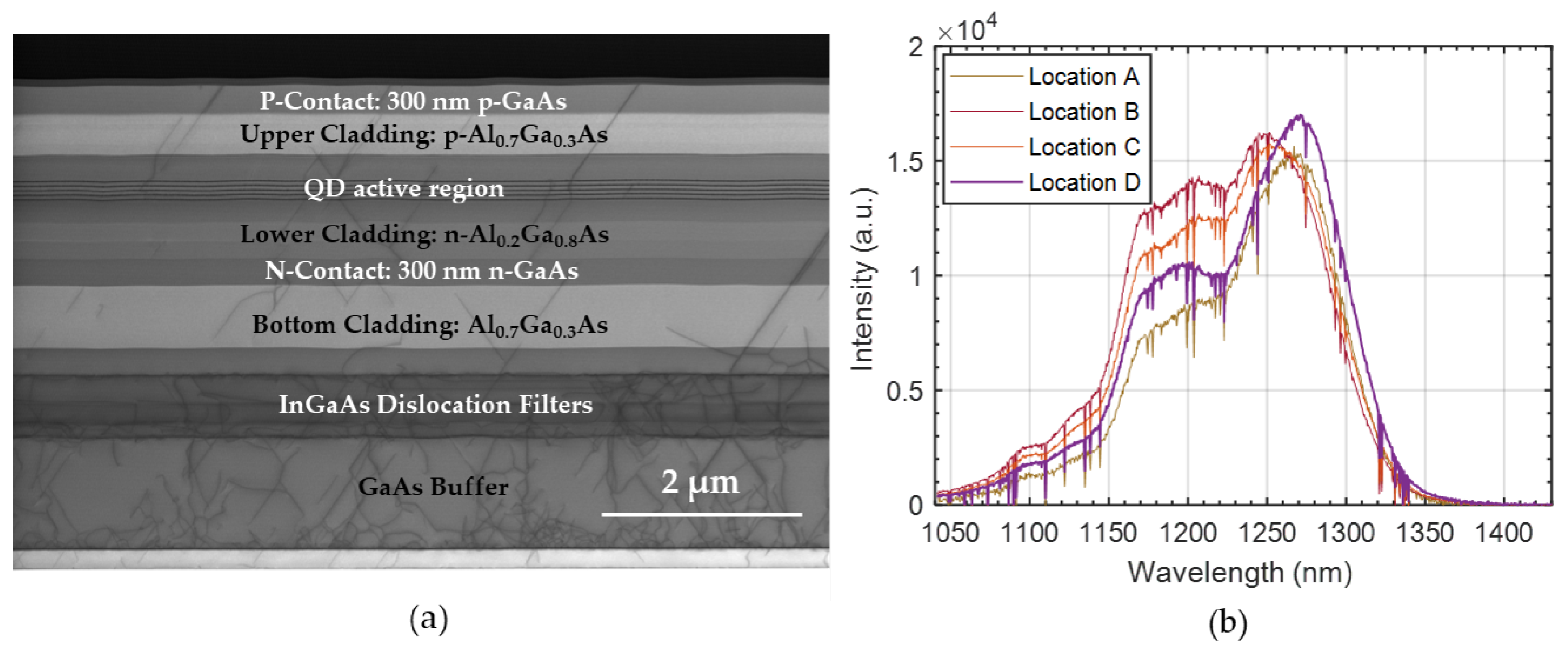
Figure 2a shows cross-section scanning transmission electron microscopy (STEM) prepared from the 300 mm wafer, where critical layer compositions and their thicknesses are marked. We estimate the threading-dislocation density (TDD) in the active region to be around cm measured by TEM.
Figure 2b shows the photoluminescence (PL) measurements across different locations of the same 300 mm wafer. Clear peaks of QD emission around 1300 nm as well as 1200 nm can be found, with slight variations around 50 nm for the peak positions. The target QD emission wavelength for O-band applications was successfully demonstrated, though there appeared to be concerns to a limited extent regarding MBE growth uniformity on the 300 mm scale, compared to the higher uniformity typical with smaller templates. We attribute the slight wavelength variation mostly to local temperature differences across the wafer.
3. In-Pocket Growth of Quantum Dot Lasers on 300 mm Si Photonic Wafer
For in-pocket growth, the laser stack is the same as planar growth described in the previous section, taking advantage of the reduced overall thickness for the vertical alignment of the active region to the in-plane SiN waveguides embedded in the patterned wafer.
The template was prepared using a 300 mm SOI wafer with SiN/Si waveguides and other passive elements. On the SOI wafer, 4.5 µm SiO2 was deposited to embed the waveguides. Dry etch patterning of SiO2 followed by additional Si recess was performed to prepare narrow rectangular pockets for the III-V material growth, enabling in-plane on-chip butt-coupling of a QD laser to SiN waveguides. After that, another thin SiO2 layer was deposited to protect the vertical Si sidewall within the recess, preparing the wafer for heteroepitaxial growth. At NAsPIII–V GmbH, the in-pocket Si surface was etched back with HCl and selectively refilled to the previous level after a high-temperature heat treatment, and the template was grown in a similar manner to the planar wafer with MOCVD. With the finished template, the MBE growth of subsequent layers was carried out in a 300 mm reactor at IQE, Inc. Details of the MBE growth development for in-pocket templates can be found in [38].
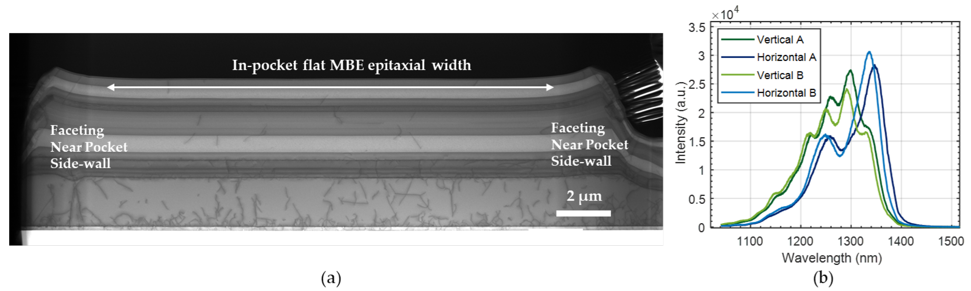
Figure 3a shows cross-section STEM of the in-pocket crystal growth for a pocket width of 20 µm. Despite clear faceting of roughly 4 µm on each side near the pocket sidewall, the central region shows a flat-top epitaxial stack that is comparable to planar growth and ready for ridge waveguide fabrication with electrical contacts. The faceting was formed due to interaction with the oxide sidewalls and polycrystalline material at the pocket edges during MBE growth, yet its effect is present only locally near the pocket sidewalls. We have observed great consistency in the MBE stack thickness across the 300 mm wafer despite various splits of pocket widths, lengths and local densities, which demonstrates the low geometry dependency of growth rate with MBE. This makes it a natural straightforward choice for large-scale integration with various growth pockets catering to specific system designs and applications. The TDD in the active region of this sample was estimated to be roughly cm.
Figure 3b shows the PL measurement across different pockets of the same wafer. Strong PL around the O-band can be observed across the wafer, again showing the robustness of MBE-grown quantum dot formation and the relatively low dependency of growth rate on geometry. For different pocket sizes and orientations, lasing peaks were observed around 1200 nm to 1350 nm. “Vertical” indicates measurements taken from pocket’s longitudinal direction aligned to the [1 1 0] III–V crystal orientation, and “horizontal” for those aligned to the [1 0] III–V crystal orientation. PL uniformity across the wafer is also good, as shown in location A and location B, which are from the same pocket size and orientation but different areas of the wafer, roughly 150 mm apart. This exciting observation shows the possibility of tailoring a specific pocket design for high-uniformity quantum dot growth quality with a given wavelength at controlled spots on large-scale photonic wafers. In addition, further applications such as on-chip tunable lasers or laser arrays with groups of wavelengths of a wide tuning range may be made possible through careful engineering. Detailed studies of the correlation between quantum dot formation and pocket design are being prepared for submission [39].
4. Fabrication Process Development of Quantum Dot Lasers
We fabricated ridge waveguide Fabry–Perot cavities for electrically pumped quantum dot lasers from the grown wafers, where Figure 4 shows a simplified view of the fabrication process for both planar and in-pocket lasers. The 300 mm wafers were cleaved or diced into smaller pieces for processing at the UCSB Nanofab facility.
Ridge waveguides were made with p-contact (Pd/Ti/Pd/Au) on top and n-contact (Pd/Ge/Au) on one side. Alternative designs of the symmetric formation of two n-contacts can also be implemented, but were not performed here. Non-Au contacts have been developed [40] but were not used here. The Cl2/N2-based dry etching to form the mesa of the ridge waveguide was developed with an in-situ laser monitor to ensure the precise control of etch depth and properly expose the thin n-contact layer. Further refinement of etching temperature, pressure and bias setting yielded vertical side walls for better device performance. After n-contact deposition, a via-opening etch was performed to lay out the deposition of electrical pads for probing on the wafer top surface for both the anode and the cathode from each side of the laser ridge.
For the in-pocket grown wafer, we added a post-MBE-growth wet-etch process to remove the surface polycrystal for sample planarization before the standard fabrication steps, which enables better focus calibration in the photolithography steps and reduces step height. In addition, several process developments were carried out to tackle challenges from high-aspect-ratio pocket sidewalls in critical steps such as etch-stop control of the mesa dry-etch, passivation coverage through narrow deep trenches and for making electrical contacts across steep sidewalls. Details of the fabrication steps can also be found in [38].
After probe deposition, the samples were thinned down to about 150 µm to 200 µm from the backside Si substrate with a mechanical polisher, and mirror facets of the cavities were made by precise cleaving. No reflective coating was applied to the samples at this stage. Typical cavity lengths were cleaved to be 1 mm to 2 mm for a systematic comparison across the two wafers and with our previous studies of quantum dot lasers on Si grown at a smaller scale [33,38].
5. Results and Discussion
5.1. Planar-Growth Quantum Dot Lasers
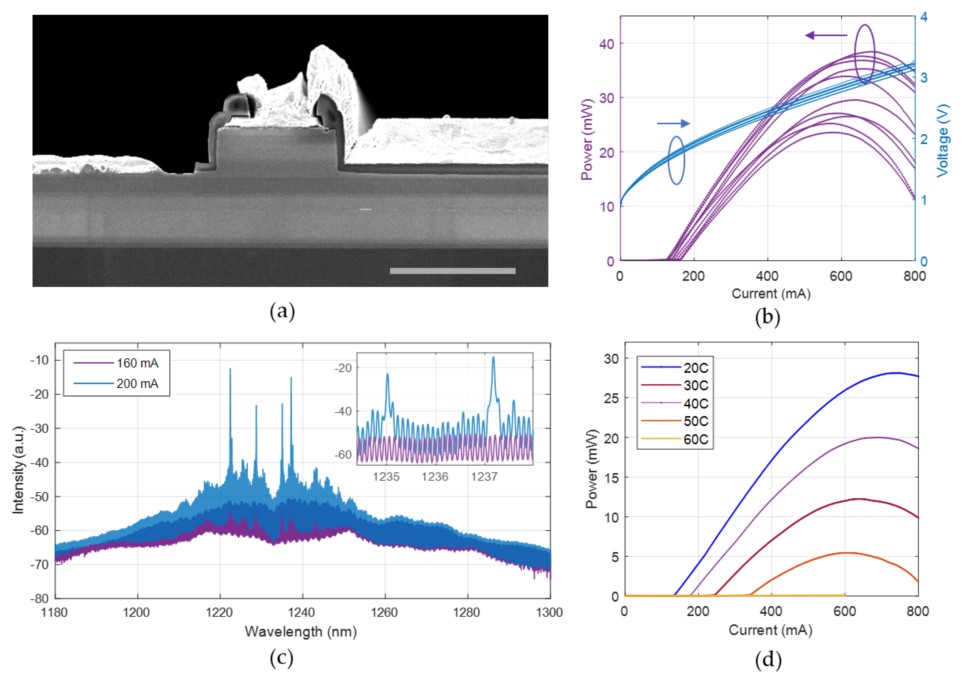
Figure 5a shows the cross-section SEM of a laser fabricated from planar growth with a ridge width of 5 µm. Figure 5b shows the light–current–voltage (LIV) measurement of ten devices from the same bar under continuous wave (CW) current injection. The optical output power was collected from a single facet with an integration sphere placed adjacent to the laser bar on the testing stage. The maximum output power of each device from a single side varies between 20 and 40 mW for ridge widths around 3–5 µm, yet some performance variation can also be attributed to slight variations in fabrication. We achieved 100% yield on some bars, though device performance varies with each design. The length of this bar is 1.5 mm, and bars of 2 mm show similar results. Device series resistance is around 2 Ω.
Figure 5c shows the spectra collected from a lensed fiber at the cleaved facet of a laser under CW current injection. This laser has a ridge width of 4 µm and a cavity length of 2 mm, and the testing stage is uncooled in a room-temperature environment. We show a spectrum of injection currents of 160 mA and 200 mA, which are below and above the lasing threshold of this device, respectively. At 200 mA, multi-mode lasing near 1230 nm can be observed, corresponding to the shorter-wavelength peaks in the PL measurement results shown in Figure 2b. The predominance of excited-state lasing is expected given the competitive PL intensity of excited states compared to the ground state, as well as the higher threshold current density of these lasers. From the zoom-in figure in the inset, mode spacing corresponding to a Fabry–Perot laser with cavity length of 2 mm is observed. Figure 5d shows device performance at different temperatures. We achieved CW lasing up to over 50 °C.
For QD lasers grown on 300 mm planar templates on Si wafers, device performance can be further tuned through different epitaxial designs, such as using thicker AlGaAs cladding layers, as previously reported in [33]. Additional growth condition optimization, such as optimizing trapping layer design or incorporating thermal cyclic annealing will improve the growth quality, which should lead to better overall performance.
With different structural designs in fabrication, one can achieve a versatile collection of lasers with various functionalities, such as using a shallow-etch ridge waveguide for higher maximum output power, adding an isolation etch for mode-locked lasers, or implementing gratings along the cavity for single-mode distributed-feedback lasers.
5.2. In-Pocket Quantum Dot Lasers
Figure 6a shows the cross-section SEM of a laser fabricated from in-pocket template with a ridge width of 5 µm in a pocket width of 30 µm. One can see how faceting near the sidewall in MBE growth would have a critical effect on ridge laser fabrication when the pocket width is relatively small. While this tight constraint can be alleviated by adjusting the pocket width and tuning growth conditions of the MOCVD template and MBE in-pocket growth accordingly, we were also able to demonstrate that by properly adjusting the ridge position, contact window and fabrication conditions, the resulting device ridge waveguide structure can be comparable to that made from a planar growth for smaller trench widths of 20 µm and even 15 µm.
The LIV in Figure 6b shows the performance of different devices on the same sample. CW current sweeping was performed to show roll-over for a record high maximum power output of each laser. Maximum single-side optical power varies from 10 mW to nearly 70 mW, and this is collectively a result of experimental parameter splits in device widths and lengths and pocket designs. These devices were measured from the pockets of the “vertical” orientation. Since the in-pocket growth conditions can be optimized for a given pocket size on a given template, with a parallel effort, high-yield fabrication with excellent lasing performance can be reliably achieved with careful down-selection of the best working parameters such as ridge width and contact distance for that given pocket size. Such learning with a short turn-around time on small samples can be a cost-effective learning path for future technology transfer to enable a 300 mm-scale III–V run-path of laser fabrication in an integrated photonics foundry.
Figure 6c shows the spectra collected from a lensed fiber at the cleaved facet of an in-pocket device with injection currents of 40 mA and 60 mA, below and above the lasing threshold, respectively. A clear peak of lasing near 1300 nm can be observed at a 60 mA injection current. The zoom-in figure shows the mode spacing of the Fabry–Perot cavity as expected. We did also observe variation in the lasing wavelengths for different in-pocket lasers, some of which were centered at a shorter wavelength near 1250 nm or 1200 nm, showing good consistency with the in-pocket PL measurements presented in Figure 3b.
Figure 6d shows the temperature-dependent performance of a laser where CW lasing was demonstrated up to 60 °C. This slightly improved thermal performance compared to the planar growth laser, which can be attributed to the lower TDD in the in-pocket growth, yet more investigation is needed for a definitive conclusion. Nevertheless, further improvement in thermal performance can also be achieved through other aspects such as optimization of the epitaxial layer stack as well as alternative device designs for more efficient heat dissipation.
5.3. On-Chip In-Pocket Quantum Dot Lasers for Si Photonic Integration
In order to demonstrate the concept of using quantum dot lasers as an on-chip integrated light source at wafer scale, we also demonstrated a laser grown in-pocket without cleaved facets. As shown in the inset of Figure 7a, we used a focused ion beam (FIB) milling process to fabricate rectangular vertical trenches on both ends of the pocket, forming highly reflective mirrors.
The laser cavity was adjacent to SiN waveguides that are vertically aligned on the same chip next to the pocket, guiding the coupled light towards an edge coupler that was diced and polished for fiber coupling. The optical microscope photo in Figure 7a shows the sample in the testing stage probed on both sides of the ridge waveguide, with bright contrast along the ridge due to light scattered off-chip as an injection current beyond the lasing threshold was being applied. The lasing performance was characterized using an integration sphere adjacent to the edge coupler, and the results in Figure 7b,c show the LIV collected from both sides of the integrated chip. To qualitatively demonstrate a proof of concept of on-chip light coupling between the QD laser and the SiN waveguide, an image was taken through a 20× objective towards the sample edge, as shown in Figure 7d. Through careful adjustment of the focal plane, one can observe a clear indication of the waveguide-coupled output of light, indicated by the orange arrow on the right, distinct from the scattered light (green arrow).
By incorporating additional dry- and/or wet-etch steps in the device fabrication process, on-chip cavity mirrors can be formed with a scalable approach in the replacement of the FIB milling process, as demonstrated in this recent work [23]. The complication of the facet etching step is also related to the bent edges as well as polycrystalline deposition near the oxide side wall, as presented in Figure 3a. With the development of the etching process as well as further research on mitigating the effect of polycrystalline deposition through partially selective MBE growth, monolithically integrated on-chip lasers with higher coupling efficiency can be realized at a large scale.
5.4. Towards the Fully Monolithic Integration of Quantum Dot Lasers with Si Photonics
Figure 8 shows the perspective of the fully monolithic integration of quantum dot lasers with Si photonics. A conceptual demonstration is shown as an example in the cross-section schematic in Figure 8a. With key developments demonstrated in previous sections of this manuscript, we envision the development of efficient in-plane butt-coupling from the active region to the passive waveguides with the in-pocket growth platform. In this schematic, we show quantum dot lasers coupled to SiN waveguides and Si waveguides, integrated with Si-based modulators, Ge-on-Si photodetectors and so on. For a monolithically integrated wafer, vertical couplers can best provide a wafer-scale testing capability, but the wafers can also be sequentially diced into smaller units with edge couplers for fiber-coupled individual packaging and their applications.
In Figure 8b, we show the top-view schematic of compact photonic integrated circuits made with pocket arrays on the same wafer. The compact arrangement of pockets with thick oxide sidewalls, on the one hand, undeniably complicates growth and fabrication to an extent, yet such challenges have been proved to be surmountable. When compared to planar growth or a larger growth window on Si, such an array of growth pockets offers unparalleled potential in photonic circuit design, where a seamless integration of on-chip active and passive components on the same chip with a high degree of freedom can be made possible without much compromise for design constraints or the requirement of complex routing.
As shown in the photograph in Figure 8c, with developed in-pocket direct heteroepitaxial growth adding to existing CMOS-compatible Si photonic process, large-scale photonic circuits with on-chip lasers for various applications and potentially from different design parties through the MPW service with photonic foundries can readily be produced at low cost and large scale.
6. Conclusions
We demonstrate for the first time quantum dot lasers grown on 300 mm Si photonic wafers from both planar template growth and in-pocket growth on patterned templates, with the material quality ready for large-scale laser fabrication and system integration. We have shown the merits of quantum dots’ tolerance to crystalline defects as an efficient gain material, and demonstrated the repeatability of MBE growth conditions irrespective of wafer sizes. Planar growth shows high quantum dot uniformity across the wafer and high yield in edge-facet laser fabrication, which is a critical step in the cost reduction and scaling of monolithically integrated III–V on Si light sources. In-pocket growth shows the robustness of quantum dot formation with different templates as well as the potential of the supreme versatility of material quality optimization in accordance with different pocket sizes and orientations.
In particular, we also demonstrate the proof of concept of on-chip coupling from in-pocket QD lasers to SiN waveguides, showing the advantage of the vertical alignment and compact arrangement of the active region and passive components on this platform. This is a vital first step that reveals the true potential of the monolithic integration of lasers on Si. With continuing efforts in further developing a wafer-scale fabrication process for efficient on-chip coupling, we envision the implementation of fully monolithically integrated photonic systems in the foreseeable future.
Author Contributions
Conceptualization, J.B., K.F. and C.S.; methodology, K.F. and C.S.; software, K.F.; validation, K.F., C.S. and E.H.; resources, C.S., A.C., K.F., P.L. and R.K.; formal analysis, K.F.; investigation, K.F., E.H. and R.K.; data curation, K.F.; writing—original draft preparation, K.F.; writing—review and editing, J.B., K.F., C.S., E.H. and R.K.; visualization, K.F.; project administration, J.B. and D.H., supervision, J.B., funding acquisition, J.B. All authors have read and agreed to the published version of the manuscript.
Funding
This material is based on research sponsored by the DARPA MTO LUMOS program under contract 442650-59747 and by the Air Force Research Laboratory under agreement number FA8650-21-2-1000. The U.S. Government is authorized to reproduce and distribute reprints for governmental purposes notwithstanding any copyright notation thereon. The views and conclusions contained herein are those of the authors and should not be interpreted as necessarily representing the official policies or endorsements, either expressed or implied, of the United States Air Force, the Air Force Research Laboratory or the U.S. Government.
Institutional Review Board Statement
Not applicable.
Informed Consent Statement
Not applicable.
Data Availability Statement
The data presented in this study may be available upon reasonable request from the authors.
Acknowledgments
We thank Mario Dumont, MJ Kennedy, Warren Jin, Andy Netherton and Joel Guo for useful discussions and help with the fabrication and testing. A portion of this work was performed in the UCSB Nanofabrication Facility, an open access laboratory.
Conflicts of Interest
JEB is a cofounder of Quintessent.
References
- Margalit, N.; Xiang, C.; Bowers, S.M.; Bjorlin, A.; Blum, R.; Bowers, J.E. Perspective on the future of silicon photonics and electronics. Appl. Phys. Lett. 2021, 118, 220501. [Google Scholar] [CrossRef]
- Thomson, D.; Zilkie, A.; Bowers, J.E.; Komljenovic, T.; Reed, G.T.; Vivien, L.; Marris-Morini, D.; Cassan, E.; Virot, L.; Fédéli, J.M.; et al. Roadmap on silicon photonics. J. Opt. 2016, 18, 073003. [Google Scholar] [CrossRef]
- Shi, Y.; Zhang, Y.; Wan, Y.; Yu, Y.; Zhang, Y.; Hu, X.; Xiao, X.; Xu, H.; Zhang, L.; Pan, B. Silicon photonics for high-capacity data communications. Photonics Res. 2022, 10, A106–A134. [Google Scholar] [CrossRef]
- Dumont, M.; Liu, S.; Kennedy, M.; Bowers, J. High-efficiency quantum dot lasers as comb sources for DWDM applications. Appl. Sci. 2022, 12, 1836. [Google Scholar] [CrossRef]
- Xie, W.; Xiang, C.; Chang, L.; Jin, W.; Peters, J.; Bowers, J.E. Silicon-integrated nonlinear III–V photonics. Photonics Res. 2022, 10, 535–541. [Google Scholar] [CrossRef]
- Zhang, X.; Kwon, K.; Henriksson, J.; Luo, J.; Wu, M.C. A large-scale microelectromechanical-systems-based silicon photonics LiDAR. Nature 2022, 603, 253–258. [Google Scholar] [CrossRef]
- Moody, G.; Sorger, V.J.; Blumenthal, D.J.; Juodawlkis, P.W.; Loh, W.; Sorace-Agaskar, C.; Jones, A.E.; Balram, K.C.; Matthews, J.C.; Laing, A.; et al. 2022 Roadmap on integrated quantum photonics. J. Phys. Photonics 2022, 4, 012501. [Google Scholar] [CrossRef]
- Siew, S.Y.; Li, B.; Gao, F.; Zheng, H.Y.; Zhang, W.; Guo, P.; Xie, S.W.; Song, A.; Dong, B.; Luo, L.W.; et al. Review of silicon photonics technology and platform development. J. Light. Technol. 2021, 39, 4374–4389. [Google Scholar] [CrossRef]
- Giewont, K.; Nummy, K.; Anderson, F.A.; Ayala, J.; Barwicz, T.; Bian, Y.; Dezfulian, K.K.; Gill, D.M.; Houghton, T.; Hu, S.; et al. 300-mm monolithic silicon photonics foundry technology. IEEE J. Sel. Top. Quantum Electron. 2019, 25, 1–11. [Google Scholar] [CrossRef]
- Munoz, P.; van Dijk, P.W.; Geuzebroek, D.; Geiselmann, M.; Dominguez, C.; Stassen, A.; Doménech, J.D.; Zervas, M.; Leinse, A.; Roeloffzen, C.G.; et al. Foundry developments toward silicon nitride photonics from visible to the mid-infrared. IEEE J. Sel. Top. Quantum Electron. 2019, 25, 1–13. [Google Scholar] [CrossRef]
- Fahrenkopf, N.M.; McDonough, C.; Leake, G.L.; Su, Z.; Timurdogan, E.; Coolbaugh, D.D. The AIM photonics MPW: A highly accessible cutting edge technology for rapid prototyping of photonic integrated circuits. IEEE J. Sel. Top. Quantum Electron. 2019, 25, 1–6. [Google Scholar] [CrossRef]
- Han, Y.; Park, H.; Bowers, J.; Lau, K.M. Recent advances in light sources on silicon. Adv. Opt. Photonics 2022, 14, 404–454. [Google Scholar] [CrossRef]
- Liang, D.; Bowers, J.E. Recent progress in heterogeneous III-V-on-silicon photonic integration. Light. Adv. Manuf. 2021, 2, 59–83. [Google Scholar] [CrossRef]
- Matsuo, S.; Aihara, T.; Hiraki, T.; Maeda, Y.; Kishi, T.; Fujii, T.; Takeda, K.; Kakitsuka, T. Heterogeneously Integrated Membrane III–V Compound Semiconductor Devices With Silicon Photonics Platform. IEEE J. Sel. Top. Quantum Electron. 2022, 29, 1–10. [Google Scholar] [CrossRef]
- Uzun, A.; Atar, F.B.; Iadanza, S.; Loi, R.; Zhang, J.; Roelkens, G.; Krestnikov, I.; Rimböck, J.; O’Faolain, L.; Corbett, B. Integration of Edge-Emitting Quantum Dot Lasers with Different Waveguide Platforms using Micro-Transfer Printing. IEEE J. Sel. Top. Quantum Electron. 2023, 29, 1–10. [Google Scholar] [CrossRef]
- Corbett, B.; Loi, R.; O’Callaghan, J.; Roelkens, G. Transfer printing for silicon photonics. In Semiconductors and Semimetals; Elsevier: Amsterdam, The Netherlands, 2018; Volume 99, pp. 43–70. [Google Scholar]
- Fathololoumi, S.; Hui, D.; Jadhav, S.; Chen, J.; Nguyen, K.; Sakib, M.; Li, Z.; Mahalingam, H.; Amiralizadeh, S.; Tang, N.N.; et al. 1.6 Tbps silicon photonics integrated circuit and 800 Gbps photonic engine for switch co-packaging demonstration. J. Light. Technol. 2020, 39, 1155–1161. [Google Scholar] [CrossRef]
- Shi, Y.; Wang, Z.; Van Campenhout, J.; Pantouvaki, M.; Guo, W.; Kunert, B.; Van Thourhout, D. Optical pumped InGaAs/GaAs nano-ridge laser epitaxially grown on a standard 300-mm Si wafer. Optica 2017, 4, 1468–1473. [Google Scholar] [CrossRef]
- Shi, B.; Pinna, S.; Zhao, H.; Zhu, S.; Klamkin, J. Lasing characteristics and reliability of 1550 nm laser diodes monolithically grown on silicon. Phys. Status Solidi A 2021, 218, 2000374. [Google Scholar] [CrossRef]
- Shi, B.; Song, B.; Taylor, A.A.; Brunelli, S.S.; Klamkin, J. Selective area heteroepitaxy of low dislocation density antiphase boundary free GaAs microridges on flat-bottom (001) Si for integrated silicon photonics. Appl. Phys. Lett. 2021, 118, 122106. [Google Scholar] [CrossRef]
- Yang, J.; Liu, Z.; Jurczak, P.; Tang, M.; Li, K.; Pan, S.; Sanchez, A.; Beanland, R.; Zhang, J.C.; Wang, H.; et al. All-MBE grown InAs/GaAs quantum dot lasers with thin Ge buffer layer on Si substrates. J. Phys. Appl. Phys. 2020, 54, 035103. [Google Scholar] [CrossRef]
- Zhang, Z.; Shang, C.; Norman, J.C.; Koscica, R.; Feng, K.; Bowers, J.E. Monolithic passive- Active integration of epitaxially grown quantum dot lasers on silicon. Phys. Status Solidi A 2022, 219, 2100522. [Google Scholar] [CrossRef]
- Wei, W.-Q.; He, A.; Yang, B.; Wang, Z.-H.; Huang, J.-Z.; Han, D.; Ming, M.; Guo, X.; Su, Y.; Zhang, J.-J.; et al. Monolithic integration of embedded III–V lasers on SOI. Light. Sci. Appl. 2023, 12, 84. [Google Scholar] [CrossRef]
- Wang, Y.; Ma, B.; Li, J.; Liu, Z.; Jiang, C.; Li, C.; Liu, H.; Zhang, Y.; Zhang, Y.; Wang, Q.; et al. InAs/GaAs quantum-dot lasers grown on on-axis Si (001) without dislocation filter layers. Opt. Express 2023, 31, 4862–4872. [Google Scholar] [CrossRef]
- Liu, A.Y.; Zhang, C.; Norman, J.; Snyder, A.; Lubyshev, D.; Fastenau, J.M.; Liu, A.W.; Gossard, A.C.; Bowers, J.E. High performance continuous wave 1.3 μ m quantum dot lasers on silicon. Appl. Phys. Lett. 2014, 104, 041104. [Google Scholar] [CrossRef]
- Ledentsov, N.N.; Kovsh, A.R.; Zhukov, A.E.; Maleev, N.A.; Mikhrin, S.S.; Vasil’ev, A.P.; Semenova, E.S.; Maximov, M.V.; Shernyakov, Y.M.; Kryzhanovskaya, N.V.; et al. High performance quantum dot lasers on GaAs substrates operating in 1.5 μm range. Electron. Lett. 2003, 39, 1126–1128. [Google Scholar] [CrossRef]
- Ouyang, D.; Ledentsov, N.N.; Bimberg, D.; Kovsh, A.R.; Zhukov, A.E.; Mikhrin, S.S.; Ustinov, V.M. High performance narrow stripe quantum-dot lasers with etched waveguide. Semicond. Sci. Technol. 2003, 18, L53. [Google Scholar] [CrossRef]
- Ledentsov, N.N.; Shchukin, V.A.; Kettler, T.; Posilovic, K.; Bimberg, D.; Karachinsky, L.Y.; Gladyshev, A.Y.; Maximov, M.V.; Novikov, I.I.; Shernyakov, Y.M.; et al. MBE-grown metamorphic lasers for applications at telecom wavelengths. J. Cryst. Growth 2007, 301, 914–922. [Google Scholar] [CrossRef]
- Kettler, T.; Karachinsky, L.Y.; Ledentsov, N.N.; Shchukin, V.A.; Fiol, G.; Kuntz, M.; Lochmann, A.; Schulz, O.; Reissmann, L.; Posilovic, K.; et al. Degradation-robust single mode continuous wave operation of 1.46 μ m metamorphic quantum dot lasers on GaAs substrate. Appl. Phys. Lett. 2006, 89, 041113. [Google Scholar] [CrossRef]
- Selvidge, J.; Norman, J.; Salmon, M.E.; Hughes, E.T.; Bowers, J.E.; Herrick, R.; Mukherjee, K. Non-radiative recombination at dislocations in InAs quantum dots grown on silicon. Appl. Phys. Lett. 2019, 115, 131102. [Google Scholar] [CrossRef]
- Liu, Z.; Hantschmann, C.; Tang, M.; Lu, Y.; Park, J.S.; Liao, M.; Pan, S.; Sanchez, A.; Beanland, R.; Martin, M.; et al. Origin of defect tolerance in InAs/GaAs quantum dot lasers grown on silicon. J. Light. Technol. 2019, 38, 240–248. [Google Scholar] [CrossRef]
- Jung, D.; Zhang, Z.; Norman, J.; Herrick, R.; Kennedy, M.; Patel, P.; Turnlund, K.; Jan, C.; Wan, Y.; Gossard, A.C.; et al. Highly reliable low-threshold InAs quantum dot lasers on on-axis (001) Si with 87% injection efficiency. ACS Photonics 2017, 5, 1094–1100. [Google Scholar] [CrossRef]
- Shang, C.; Hughes, E.; Wan, Y.; Dumont, M.; Koscica, R.; Selvidge, J.; Herrick, R.; Gossard, A.C.; Mukherjee, K.; Bowers, J.E. High-temperature reliable quantum-dot lasers on Si with misfit and threading dislocation filters. Optica 2021, 8, 749–754. [Google Scholar] [CrossRef]
- Shang, C.; Selvidge, J.; Hughes, E.; Norman, J.C.; Taylor, A.A.; Gossard, A.C.; Mukherjee, K.; Bowers, J.E. A Pathway to Thin GaAs Virtual Substrate on On-Axis Si (001) with Ultralow Threading Dislocation Density. Phys. Status Solidi A 2021, 218, 2000402. [Google Scholar] [CrossRef]
- Selvidge, J.; Hughes, E.T.; Norman, J.C.; Shang, C.; Kennedy, M.; Dumont, M.; Netherton, A.M.; Zhang, Z.; Herrick, R.W.; Bowers, J.E.; et al. Reduced dislocation growth leads to long lifetime InAs quantum dot lasers on silicon at high temperatures. Appl. Phys. Lett. 2021, 118, 192101. [Google Scholar] [CrossRef]
- Volz, K.; Beyer, A.; Witte, W.; Ohlmann, J.; Németh, I.; Kunert, B.; Stolz, W. GaP-nucleation on exact Si (0 0 1) substrates for III/V device integration. J. Cryst. Growth 2011, 315, 37–47. [Google Scholar] [CrossRef]
- Beyer, A.; Stegmüller, A.; Oelerich, J.O.; Jandieri, K.; Werner, K.; Mette, G.; Stolz, W.; Baranovskii, S.D.; Tonner, R.; Volz, K. Pyramidal structure formation at the interface between III/V semiconductors and silicon. Chem. Mater. 2016, 28, 3265–3275. [Google Scholar] [CrossRef]
- Shang, C.; Feng, K.; Hughes, E.T.; Clark, A.; Debnath, M.; Koscica, R.; Leake, G.; Herman, J.; Harame, D.; Ludewig, P.; et al. Electrically pumped quantum-dot lasers grown on 300 mm patterned Si photonic wafers. Light. Sci. Appl. 2022, 11, 299. [Google Scholar] [CrossRef]
- Shang, C.; Hughes, E.T.; Begley, M.R.; Koscica, R.; Fouchier, M.; Wang, F.; Dai, H.; Mukherjee, K.; Feng, K.; He, W.; et al. Design rules for addressing material asymmetry induced by templated epitaxy in pockets for on-chip heteroepitaxial light sources. ACS Nano 2023, submitted.
- Jain, S.; Sysak, M.; Swaidan, M.; Bowers, J. Silicon fab-compatible contacts to n-InP and p-InGaAs for photonic applications. Appl. Phys. Lett. 2012, 100, 201103. [Google Scholar] [CrossRef]
Figure 1.
Direct MBE growth of quantum dot lasers on 300 mm Si wafers and sample preparation for electrically pumped edge-emitting ridge waveguide lasers. Upper figures show the preparation of a planar Si template and fabrication of edge-emitting ridge waveguide lasers; lower figures show the preparation of a patterned template with compact pockets for edge-emitting lasers and on-chip integrated lasers.

Figure 2.
Characterization of quantum dot epitaxial growth on a planar 300 mm Si wafer: (a) Cross-section STEM of the laser stack. (b) Photoluminescence (PL) characterization of the as-grown wafer.
Figure 2.
Characterization of quantum dot epitaxial growth on a planar 300 mm Si wafer: (a) Cross-section STEM of the laser stack. (b) Photoluminescence (PL) characterization of the as-grown wafer.

Figure 3.
Characterization of quantum dot epitaxial growth in-pockets on 300 mm Si photonic wafer: (a) Cross-section STEM of the epitaxial layers in a pocket of around 20 µm width. (b) PL characterization of the as-grown in-pocket material.
Figure 3.
Characterization of quantum dot epitaxial growth in-pockets on 300 mm Si photonic wafer: (a) Cross-section STEM of the epitaxial layers in a pocket of around 20 µm width. (b) PL characterization of the as-grown in-pocket material.

Figure 4.
Fabrication process of electrically pumped Fabry–Perot cavity lasers on (a) blanket growth wafer and (b) in-pocket growth wafer.
Figure 4.
Fabrication process of electrically pumped Fabry–Perot cavity lasers on (a) blanket growth wafer and (b) in-pocket growth wafer.

Figure 5.
Characterization of quantum dot lasers grown and fabricated on a planar template on Si: (a) Scanning electron microscopy (SEM) image of the facet of a laser with mesa width around 5 µm. Scale bar is 5 µm. (b) Single-side, continuous wave (CW) light–current–voltage (LIV) measurement of several lasers from a single bar. (c) Spectrum of a laser at injection currents below (purple) and above (blue) the lasing threshold. Inset shows zoom-in details near 1236 nm. (d) Temperature-dependent light–current measurement of a laser.

Figure 6.
Characterization of quantum dot lasers grown and fabricated with an in-pocket template on Si: (a) SEM image of the facet of a laser with mesa width around 5 µm in a pocket of 30 µm in width. Scale bar is 5 µm. (b) Single-side, CW LIV measurement of a few lasers from the same sample. (c) Spectrum of a laser at injection currents below (green) and above (blue) the lasing threshold. Inset shows zoom-in details near 1300 nm. (d) Temperature-dependent light–current measurement of one laser.

Figure 7.
On-chip in-pocket quantum dot laser integrated to SiN waveguides. (a) Optical microscope photo of an on-chip in-pocket laser in the testing stage. Inset shows SEM of the milled mirror. (b) CW L-I measurement results of the lasing cavity after FIB-milled facets. (c) I–V measurement results of the cavity. (d) Waveguide-coupled output from an on-chip laser.

Figure 8.
Future of the fully monolithic integration of quantum dot lasers with Si photonics. (a) Cross-section schematic of compact heteroepitaxial integration of quantum dot lasers directly grown on Si photonic wafers. (b) Top-view schematic of pocket arrays enabling high-density integration of in-pocket active components with Si photonic elements. (c) Close-up photograph of a patterned 300 mm Si photonic wafer with lasers grown in pockets. The wafer was diced into smaller coupons in preparation for further process development and testing.

Disclaimer/Publisher’s Note: The statements, opinions and data contained in all publications are solely those of the individual author(s) and contributor(s) and not of MDPI and/or the editor(s). MDPI and/or the editor(s) disclaim responsibility for any injury to people or property resulting from any ideas, methods, instructions or products referred to in the content. |
© 2023 by the authors. Licensee MDPI, Basel, Switzerland. This article is an open access article distributed under the terms and conditions of the Creative Commons Attribution (CC BY) license (https://creativecommons.org/licenses/by/4.0/).
Share and Cite
MDPI and ACS Style
Feng, K.; Shang, C.; Hughes, E.; Clark, A.; Koscica, R.; Ludewig, P.; Harame, D.; Bowers, J. Quantum Dot Lasers Directly Grown on 300 mm Si Wafers: Planar and In-Pocket. Photonics 2023, 10, 534. https://doi.org/10.3390/photonics10050534
AMA Style
Feng K, Shang C, Hughes E, Clark A, Koscica R, Ludewig P, Harame D, Bowers J. Quantum Dot Lasers Directly Grown on 300 mm Si Wafers: Planar and In-Pocket. Photonics. 2023; 10(5):534. https://doi.org/10.3390/photonics10050534
Chicago/Turabian StyleFeng, Kaiyin, Chen Shang, Eamonn Hughes, Andrew Clark, Rosalyn Koscica, Peter Ludewig, David Harame, and John Bowers. 2023. "Quantum Dot Lasers Directly Grown on 300 mm Si Wafers: Planar and In-Pocket" Photonics 10, no. 5: 534. https://doi.org/10.3390/photonics10050534
Note that from the first issue of 2016, this journal uses article numbers instead of page numbers. See further details here.