A Concise Review of the Progress in Photonic Sensing Devices


Institute of Microelectronics and Optoelectronics, Warsaw University of Technology, Koszykowa 75, 00-662 Warszawa, Poland
*
Author to whom correspondence should be addressed.
Photonics 2023, 10(6), 698; https://doi.org/10.3390/photonics10060698
Submission received: 7 June 2023
/
Revised: 14 June 2023
/
Accepted: 19 June 2023
/
Published: 20 June 2023
(This article belongs to the Special Issue Advanced Photonic Sensing and Measurement)
Abstract
:Photonic sensing devices have become increasingly important in various fields such as agriculture, medicine, biochemical sensing, and manufacturing. They are highly sensitive and can classify minor changes in the physical and chemical properties of the ambient medium with high precision. This makes them practical in applications where accurate measurements are critical, such as medical diagnostics and environmental monitoring. In this review paper, recent advances in different types of photonic sensors are discussed, which include photonic crystal-based sensors, surface plasmon resonance-based sensors, optical fiber-based sensors, optical waveguide-based sensors, and wearable sensors. These highly fascinating sensing devices play a crucial role in countless applications and have several advantages over traditional sensors. As technology continues to advance, we can expect photonic sensors to become even more precise, versatile, and reliable.
1. Introduction
Photonic sensors are devices that utilize light to detect and measure various physical factors such as temperature, pressure, strain, and chemical composition. They can be divided into fiber-optic-based sensors and other photonic sensors, with distributed and point sensors being the main categories. Fiber-optic-based sensors are commonly used for distributed sensing applications and rely on the propagation of light through optical fibers to measure parameters along their length. However, in this article, we will not be considering distributed sensors in detail. For a comprehensive review of distributed sensing techniques, readers are encouraged to refer to previous works [1,2,3,4] that delve into the intricacies of these methodologies. These references provide in-depth insights into the advancements and methodologies employed in the field of distributed sensing. The basic principle of photonic sensors is to detect changes in the optical properties of a material or a system caused by the parameter being measured [5,6]. For example, a photonic sensor can detect variations in the refractive index (RI), absorption, or fluorescence of a substance under observation, which can be correlated with the concentration of a target molecule or the presence of a specific substance [7,8]. They have a wide assortment of applications in different fields, containing: (I) medical applications, such as monitoring blood glucose levels, measuring oxygen saturation in blood, and detecting cancer cells [9]; (II) environmental surveillance, where these sensors can be used to monitor environmental parameters such as air and water quality, temperature, and humidity; (III) aerospace and defense: such as aircraft control systems, missile guidance, and remote sensing; (IV) structural health surveillance: photonic sensors can be employed to monitor the structural health of buildings, bridges, and other infrastructure [10,11,12]; (V) industrial process control: such as monitoring the temperature and pressure in chemical reactors and detecting gas leaks; (VI) communication networks: photonic sensors are used in communication networks for monitoring the performance of optical fibers and detecting fiber breaks; (VII) energy sector: photonic sensors can be used for surveillance of the condition of wind turbine blades, detecting pipeline leaks [13], and monitoring the temperature and pressure of oil and gas wells [14,15,16].
The future of photonic sensing technology holds great promise and is expected to bring significant advancements and applications. As the Internet of Things (IoT) continues to grow, photonic sensors will play a vital role in creating smart cities and interconnected systems [17]. Photonic sensors can enable efficient monitoring of various parameters, such as air quality, traffic flow, structural health, and energy consumption, leading to improved resource management and enhanced quality of life. Photonic sensors have immense potential in the field of biomedicine. They can be used for non-invasive and real-time monitoring of vital signs such as heart rate, blood pressure, and oxygen levels. Additionally, advancements in photonic sensing may lead to breakthroughs in imaging techniques, enabling more precise diagnostics and treatment monitoring [18,19]. With growing concerns about climate change and environmental pollution, photonic sensors can significantly contribute to monitoring and mitigating these issues. They can be employed for monitoring air and water quality, greenhouse gas emissions, and the detection of hazardous substances. They can help in the early detection and prevention of environmental hazards, leading to more effective environmental management.
Presently, traditional personal healthcare practices mostly rely on obsolete approaches, such as heavy equipment and convoluted procedures, which in certain cases can be difficult and time-consuming. Additionally, such antiquated techniques require the utilization of bulky apparatus, blood samples, and conventional bench-top testing techniques. Patients may feel uncomfortable and distressed because of intrusive methods of collecting test samples. In contrast, wearables may be fitted to a variety of body parts to record various biochemical and physiological traits as a growing analysis unit. Health is monitored using physical, chemical, and biological information that is sent via the skin under various conditions. Thanks to non-intrusive sampling and excellent precision, wearables may detect abnormalities in the physical or chemical components of the human body in real-time, exposing the bodily status over time [20,21]. The form factors of most commercially accessible wearable technology are eventually confined by the size and weight of the batteries needed for the power supply, which are mechanically hard modules attached to bands and worn on the wrist. A lot of health information is contained in basic physiological signals [22]. Evaluation of the pulsatile component of the bloodstream allows for the measurement of important physiological factors, for instance, pulse imperfection or fluctuation using photoplethysmography (PPG) and oxygen saturation in arterial blood employing pulse oximetry [23,24]. A new kind of technology called wearable devices with “skin-like” properties is only now beginning to leave research laboratories and enter pre-commercial versions. Due to their durability, lightness, mobility, and elasticity, flexible skin-like systems have accomplished several capabilities that were formerly unattainable for conventional sensing devices [25,26,27]. Shape sensing is an innovative technology that uses sensors and algorithms to accurately measure the shape, position, and movement of objects or structures. It has applications in robotics, medicine, structural monitoring, and virtual reality, providing enhanced control and efficiency [28,29].
Photonic sensors offer numerous benefits over customary sensors, such as high sensitivity, quick response times, and low power consumption [7]. These sensing devices have a faster response time than electronic sensing devices, which means they can identify variations in light more quickly. This makes them useful in applications where speed is vital, such as industrial process control or high-speed imaging [30,31]. Additionally, these sensing devices are immune to electromagnetic interference (EMI), which means they can operate in environments with high EMI, such as near power lines or industrial sites. They also have the potential for multiplexed detection of multiple parameters, which can be useful in complex sensing applications. In this chapter, six types of photonic sensing devices are briefly discussed. In Section 2, the market outlook for photonic sensors is briefly explained. In Section 3, Section 4, Section 5, Section 6 and Section 7, the recent advancements in photonic crystal, surface plasmon resonance, optical fiber, optical waveguide, and wearable sensing devices are discussed, respectively. The current challenges associated with the development of photonic sensors are briefly presented in Section 8. The paper ends with concluding remarks in Section 9.
2. Photonic Sensors Market Outlook
The revenue generated by the worldwide market for photonic sensors and detectors reached USD 35.5 billion in 2021 and reached a value of USD 38 billion in 2022. Furthermore, it is anticipated that the overall demand for photonic sensors and detectors will rise at a healthy CAGR of 8.2% between 2022 and 2032, reaching a market valuation of roughly USD 83.5 billion by that year due to growing applications in healthcare and medical, chemicals, industrial automation, and consumer electronics [32]. To improve interactions at machine/environment interfaces, photonic sensors and detectors are employed. Imaging sensor technology is being influenced by photonic sensors, which offer a low-mass and low-noise alternative to larger traditional sensors. In science, the use of sensors has become crucial for study, particularly for making invisible phenomena visible [32].
The demand for photonic sensors varies across different industry verticals such as healthcare, telecommunications, aerospace and defense, industrial automation, and environmental monitoring. The market value is driven by the adoption of photonic sensors in these sectors and their specific requirements. Advances in photonic sensor technologies, such as miniaturization, increased sensitivity, and improved performance, can drive market growth and increase the market value of these sensors. Continued research and development efforts contribute to the evolution of photonic sensors and their market value. Government initiatives and regulations that promote the adoption of photonic sensors in sectors like healthcare, energy, and environmental monitoring can positively impact their market value. Supportive policies and incentives often drive the demand for photonic sensors in these industries. The emergence of new applications, such as autonomous vehicles, the Internet of Things (IoT), and smart cities, can create new market opportunities for photonic sensors [33]. These applications require sensors with advanced capabilities, which can contribute to the market value of photonic sensors. The market value of photonic sensors can also be influenced by competition among manufacturers and suppliers. Market dynamics, including pricing strategies, product differentiation, and technological leadership, can affect the overall market value.
3. Photonic Crystals-Based Sensing Devices
A photonic crystal (PhC) surface is a type of material that consists of a periodic modulation of dielectric nanostructures. This periodic modulation causes the material to exhibit distinctive optical properties, including the competence to manipulate the propagation and interaction of light with matter [34]. PhCs are exemplified by their band structure, which is a range of energies at which light cannot propagate through the material due to the periodic modulation of the dielectric structure. This property can be utilized to create devices that manipulate light, such as filters and sensors [35,36,37]. Overall, PhCs have important applications in the fields of optics, photonics, and telecommunications [38,39]. A PhC surface can be fabricated to include photonic bandgaps that specifically prohibit light propagation at certain wavelengths [40].
Utilizing the local optical modes offered by the PhC surface, biosensing and bioimaging in life science research can be achieved through an extremely sensitive and label-free platform [41]. Label-free imaging of surface-absorbed live cells, involving observations of cell attachment, chemotaxis, and apoptosis, was conducted using the third generation of PhC-enhanced microscopy (PhCEM) [42]. PhCEM can provide detailed and dynamic information on cell-surface attachment profiles, covering biologically relevant timescales. Importantly, this technique holds the capability to observe cell behavior with adequate spatial resolution to detect attachment footprints of filopodial extensions and intracellular attachment strength gradients. Another study [43] presents a label-free biosensor imaging technique that uses a PhC surface to sense the surface connection of single dielectric and metal nanoparticles. The approach involves measuring localized shifts in the wavelength and reflection magnitude of the resonant from the PhC. The authors demonstrate that metal nanoparticles connected to the biosensor surface can be sensed by modulation of the resonant wavelength. The technique has been experimentally proven and is supported by finite difference time domain (FDTD) simulations. The imaging of individual nanoparticles could be used for single-molecule biosensing by functionalizing the particles with specific recognition molecules.
Measuring the tissues’ refractive indices is one of the fields of bio-optics’ most fascinating subjects. As a result, two new optical biosensor configurations for the detection of cancer cells have been suggested [41]. These structures are made up of two metal-insulator-metal (MIM) plasmonic waveguides (WGs) and one-dimensional PhC lattices. Additionally, in the second suggested topology, the MIM plasmonic WGs are better matched thanks to the tapering method. The PhC lattices in the middle section of the structures create photonic bandgaps with sharp edges in the transmission spectra of the biosensors. These sharp edges are good candidates for sensing applications [41].
PhCs present an exciting opportunity for developing high-performance sensing devices. PhCs offer strong optical confinement in a small area, which enables the detection of chemical analytes. Additionally, by using advanced chemical surface functionalization methods and microfluidic systems, highly efficient miniaturized sensor chips can be created. The study in [44] shows that functionalized slotted PhC cavities with integrated microfluidics, as shown in Figure 1, can detect dissolved avidin concentrations as low as 15 nM or 1 μg/mL. The cavity sensing surface area is ~2.2 μm2, and the detection of surface mass densities of order 60 pg/mm2, consistent with a bound mass of ~100 ag, is achieved. The ultra-compact size of the sensing devices makes them ideal for lab-on-a-chip utilization, where high densities of independent sensing sections are required in a small region. The high S of the sensing devices is due to the strong modal overlap with the analyte empowered by the slotted WG cavity geometry, resulting in substantial swings in the cavity peak wavelength when assessed against rival methods [44].
Various parameters, including stability, sensitivity, selectivity, and limit of detection (LoD), are evaluated to assess the functioning of optical biosensors [45]. In the case of 2D PhC, sensitivity is determined by measuring the degree of contact between light and the immediate material. This parameter is usually stated as the slightest variation in resonance wavelength (λres) divided by the difference in medium RI in nanometers per refractive index unit (nm/RIU). Sensitivity is denoted as “S” and is expressed as
where Δλ and Δn are the changes in λres and RI of the ambient medium, respectively. Selectivity is important for the biosensor to identify specific analytes in a sample. The stability of the biosensor is influenced by the surrounding medium, and LoD is used to compare the performance of different optical biosensors. The LoD is generally defined as the minimum possible variation in the RI essential to producing a noticeable adjustment in the output signal.
Researchers worldwide are conducting extensive investigations into RI sensing devices that are based on PhCs. This technology enables researchers to create optical WGs with low bending losses and extreme-low group velocity, which can be used to elaborate compact optical devices that modify the optical phase of signals passing through the WGs. One such device, the Mach-Zehnder interferometer (MZI), is particularly important as it can serve as a building module for further complex optical devices, for example, filters, demultiplexers, interleaves, modulators, switches, and gates [46,47]. In [48], the authors analyze the operation of an MZI that consists of two coupled-cavity WGs with unique lengths, designed in a two-dimensional PhC. The authors provide simulation results using an FDTD code that proves the theoretical analysis and addresses the key limits of the structure’s performance. These sensors have quite a few advantages, such as requiring minimal sample preparation without the need for fluorescence labeling and providing high sensitivity. The sensing mechanism detects changes in the RI of a bulk solution caused by the presence of chemical analytes. These sensors can be used to differentiate the concentrations of biochemical samples in both gaseous and aqueous environments. Furthermore, these sensing devices can measure the surface or volumetric density of molecules and proteins.
The sensitivity of resonant wavelengths of PhC membrane nanocavities to ambient RI is a key factor in (bio)chemical sensing. By understanding how the resonant wavelengths vary with changes in RI, these nanocavities can be used as extremely sensitive sensing devices for detecting and measuring the concentration of various chemicals and biomolecules. The authors in [49] investigated the potential of using PhC membrane nanocavities with integrated InAs quantum dots for (bio)chemical sensing. They used photoluminescence measurements to identify the resonances of different modes in various point-defect-type cavities. Their results showed that there are systematic trends of sensitivity variation with the degree of intersection of modes with the PhC holes, both within a cavity type and for varying cavity types. The highest sensitivity observed was around 300 nm/RIU, which occurred when the mode overlap with the holes was about 25% and the solution was completely infiltrated [49].
Gas sensing devices established on PhCs for the mid-infrared range have attracted attention due to their ability to identify trace gases and their potential for integration with other technologies. In these sensing devices, the PhC structure is designed to interact with specific gas molecules, causing a change in the resonant frequency of the PhC, which can be sensed and analyzed. The mid-infrared range is particularly useful for gas sensing because many gases have strong absorption features in this range, allowing for highly selective detection. The point-defect nanocavities established on Si planar PhC have been enhanced for sensing the RI of gases in the MIR wavelength zone [50]. By improving the radius and position of the air holes, the Q/V ratio for the point-defect PhC nanocavities can be strengthened, resulting in a high sensitivity of 270 nm/RIU and an LoD of 10−4 RIU for sensing the RI of gases.
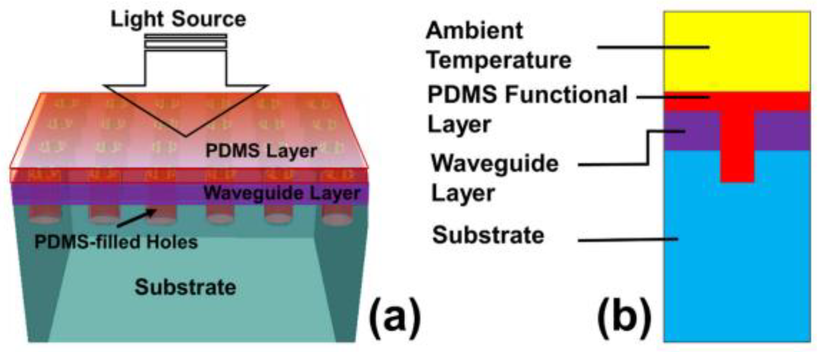
The near-infrared spectral region is examined numerically for a heat sensor based on a dielectric PhC [51]. The schematic of the PhC-based thermal sensor is shown in Figure 2a,b. A WG layer is placed on a silicon dioxide substrate, and air holes are drilled through it for easier fabrication. A functional layer of polydimethylsiloxane biguanide polymer is placed on top to sense ambient temperature; the optical characteristics of this layer change as the temperature does. Design and numerical simulation are performed using MEEP, an open-source finite-difference time-domain program. The device delivers a sensitivity value in the range of 0.109 nm/°C and a figure of merit (FOM) of 0.045 °C for an ambient temperature range of 10 to 90 °C, for which the sensor’s performance is examined. The device can be suggested for a variety of thermal sensing applications due to its high temperature tolerance, benign chemical qualities, inexpensive material cost, and ease of integration with optical fiber [51].
The fabrication of PhC structures can be complex and expensive. It often requires specialized equipment and techniques, such as electron-beam lithography (EBL) or nanoimprint lithography (NIL), which can limit their widespread adoption. PhC sensors are typically designed to operate within a specific wavelength range [52,53]. This limited range restricts their applicability to specific sensing applications and may require different designs or structures for different sensing targets. This WG configuration can be sensitive to shifts in the surrounding environment, for example, temperature, humidity, and strain. These variations can affect the RI of the materials used in the PhC structure, leading to fluctuations in the sensor’s performance and accuracy. When used for biological sensing applications, PhC sensors may face challenges due to the interaction between the sensing surface and the biological samples. Biofouling, non-specific binding, and other surface effects can affect the sensor’s performance and accuracy. Moreover, integrating PhC sensors into existing systems or devices can be challenging due to their specialized fabrication requirements and unique optical properties. This limitation may hinder their adoption in certain applications where seamless integration is crucial. Despite these disadvantages, PhC-based sensors offer unique advantages such as high sensitivity, label-free detection, and the potential for miniaturization. Ongoing research and technological advancements aim to overcome these limitations and expand the practical use of these sensors in various fields.
4. Surface Plasmon Resonance (SPR) Based Sensing Devices
Plasmonics is the study of the behavior of plasmons, which are collective oscillations of free electrons in a metal. In particular, the interaction of light with the free electrons on the surface of a metal can result in the excitation of SPs, which are waves of electron density that propagate along the metal surface [54]. SPs are collective oscillations of free electrons that can be excited on the surface of a metal [55]. These oscillations can couple with photons, resulting in strong light-matter interactions that can be exploited for various purposes. Localized surface plasmon resonances (LSPRs) are SP types that occur in small metallic nanoparticles or structures [56]. When the frequency of incident light matches the natural frequency of the LSPR, it can excite collective oscillations of free electrons within the nanoparticle, leading to strong absorption and scattering of light. LSPRs are highly dependent on the nanoparticle’s size, shape, and material, as well as the surrounding medium, making them a valuable tool for sensing and spectroscopy applications. Propagating surface plasmon polaritons (PSPPs) are hybrid waves that arise from the coupling between the EM waves in a dielectric medium and the SPs on a metal surface [57]. When the incident light’s frequency matches the SP’s natural frequency, a surface wave is generated that propagates along the metal-dielectric interface. This wave can be restrained to a sub-wavelength scale, allowing for highly efficient light-matter interactions [58]. PSPPs are used in various applications, such as nanophotonic devices, plasmonic WGs, and surface-enhanced Raman spectroscopy (SERS) [59].
SPR is a powerful tool for studying the interaction of light with matter, particularly in the field of biosensing. When the frequency of the incident light matches the natural frequency of the SP, a resonance occurs, leading to an alteration in the RI near the metal surface. This change in RI can be spotted and quantified, allowing for the detection of biomolecules and other analytes that bind to the metal surface. Plasmonic materials exhibit strong interactions between their electrons and EM radiation in the visible to near-infrared spectral range [60]. These materials typically consist of metals such as gold, silver, or copper, which have a high electron density and can support the collective oscillation of electrons known as SPs. Plasmonic materials are of great interest in the field of nanotechnology because they allow for the manipulation and control of light on a nanoscale [61].
Plasmonic sensors have significant potential for various environmental research applications due to their unique properties and capabilities. They offer the potential for real-time and continuous monitoring of environmental parameters. Their high sensitivity, fast response time, and compatibility with miniaturization enable the deployment of portable and autonomous sensor systems. Plasmonic sensors can be integrated into networks or distributed sensor arrays to provide spatially resolved and comprehensive environmental data. Plasmonic sensors can be utilized for the detection and analysis of biological entities in environmental samples. For example, they can detect and quantify specific bacteria, viruses, or biomarkers indicative of environmental contamination or ecosystem health. Plasmonic biosensors can be combined with microfluidic systems for automated sample handling and analysis, enabling rapid and sensitive environmental bioassays [62].
Plasmonic sensors can detect and analyze a wide range of environmental contaminants, including pesticides, toxins, and chemical warfare agents. The high sensitivity and selectivity of plasmonic sensors allow for the identification and quantification of these contaminants, even at trace levels. This capability is essential for environmental risk assessment and remediation efforts. They can contribute to the monitoring and analysis of atmospheric pollutants, including volatile organic compounds (VOCs) and greenhouse gases [63]. The ability of plasmonic sensors to detect low concentrations of these gases can aid in air quality assessment, climate change studies, and the development of mitigation strategies.
Prism-based SPR sensing devices are the most common type of SPR sensing device. These sensors use a thin metal film, typically made of gold or silver, coated onto a glass or prism surface. The metal film is often a few nanometers thick and is employed to excite SPs when light is directed onto it. When light is directed onto the prism, it is reflected off the metal film and interacts with the electron density at the metal surface. This interaction generates SPs, and the propagation of SPs is responsive to shifts in the RI of the medium near the metal surface. This makes SPR sensing devices useful for sensing changes in the concentration or binding of analytes near the metal surface. Prism-based SPR sensing devices are commonly used in different applications, including biomolecular interaction analysis, drug discovery, and environmental monitoring. They are extremely sensitive, label-free, and can be used to measure a broad range of analytes involving proteins, DNA, and small molecules. The detection of cancer and diabetes diseases is a crucial area of research in biosensing. To improve the accuracy of detection, researchers have introduced various methods, including the application of zinc selenide (ZnSe) semiconductor material to improve the sensitivity of a standard Ag-based SPR biosensor [64]. The suggested sensing device structure, as shown in Figure 3a is simple, economical, and simple to fabricate. In testing, the sensor detected various tumorous cells in human blood with an outstanding sensitivity of 359°/RIU and detected various glucose levels in human urine with high performance. The suggested biosensor can effectively sense distinct kinds of cancer cells and various concentrations of glucose in the urine, providing a promising avenue for disease detection. The reflection spectrum of the proposed sensor for normal MDA-MB-231 cells and cancerous cells is shown in Figure 3b. In [65], researchers proposed a sensitive prism-based SPR sensing device for sensing formalin via multilayer black phosphorous (BP). The study examines the impact of various materials on the sensor’s performance, including prism materials, metals, and 2D materials. The intended sensing device structure, consisting of BK7, silver, and nine layers of BP, achieves a sensitivity of 289.4565°/RIU and a detection accuracy (DA) of 0.3125/° for formalin detection.
Grating-coupled SPR sensors utilize a diffraction grating to couple incident light to the SP waves on a thin metal film. These sensors provide benefits over prism-based SPR sensors, including the ability to use lower-cost light sources, the ability to measure in a label-free and real-time manner, and the ability to perform multiplexed measurements. When the incident angle and wavelength match the plasmon resonance condition, a resonant coupling occurs between the incident light and the SPs, resulting in a dip in the reflected light intensity, which can be used to measure fluctuations in the RI of the metal film caused by the binding of molecules to its surface [66].
Highly efficient and compact SPR sensing devices are in high demand due to their versatility in various application scenarios when compared to traditional sensing devices. However, most compact SPR sensing devices require additional equipment like spectrometers or rotation stages to achieve high-precision spectral or angular analysis, leading to increased costs. A recent study demonstrates a low-cost and compact SPR sensor that utilizes a single grating as a coupler and a disperser [67]. The sensor utilizes a versatile digital disc-recordable disc grating to couple polychromatic light emitted from a light-emitting diode to SP modes. The same grating was used to disperse the light, which was then collected by a linear charge-coupled device. The sensor shows a high RI resolution of 5.52 × 10⁻⁵ RIU and can be employed in various fields, involving food safety, environmental examination, and medical diagnosis. A Si grating-enabled nanostructure for the sensing of RI using SPR phenomena in the NIR region is proposed [68]. The proposed structure exhibits sensitive behavior (1000 nm/RIU) for a specific range of analyte RI and accurate sensing behavior with an average quality factor value of 650 RIU−1.
Another type of SPR sensor is known as a WG-based SPR sensor, which uses a WG structure to excite SP waves on a thin metal film [69]. The sensing principle is established by the resonant coupling of the incident light with the SP waves. This dip can be used to measure the binding of molecules to the metal film surface, delivering knowledge about the concentration and affinity of the analyte molecules. WG-based SPR sensors offer several advantages, including the ability to achieve high sensitivity and selectivity, the ability to integrate with other on-chip components, and the potential for multiplexed measurements. A novel approach called a planar WG-based SPR sensing apparatus is suggested [70] using a silver-chloride material with a black phosphorus structure to sense formalin, a chemical used for food preservation that is linked to chronic cancer. The study examines the optimization of metal thickness and the chloride material’s optimal performance through transmittance power and resonance shift observations. The proposed sensing apparatus has a sensitivity of 344°/RIU, a quality factor of 166.99 RIU−1, a detection accuracy of 3.34, and a FOM of 164.74 [70]. The researchers proposed a novel WG-based SPR sensor consisting of graphene/Au/SiC layers that can work in the visible and NIR wavelength ranges [71]. The cross-sectional schematic of the sensor is explained in Figure 4. The sensitivity of the sensor was characterized, and the study showed that increasing the graphene layers improved the sensitivity. With 10 graphene layers, the sensor achieved a sensitivity of 2810 nm/RIU. The sensing apparatus has the potential for use in portable biosensors for various biological and chemical sensing applications [1].
Two-dimensional materials, such as graphene, transition metal dichalcogenides (TMDs), and black phosphorus, offer several advantages that can improve the sensitivity of sensors [72,73,74]. The ultrathin nature of 2D materials enables them to be placed near the sensing elements, resulting in improved sensitivity [75]. This proximity enhances the interaction between the analyte and the material, leading to a more sensitive detection or measurement. Two-dimensional materials possess an extremely high surface-to-volume ratio due to their atomic-thin structure. This large surface area allows for greater interaction with the surrounding environment, enhancing the chances of detecting and capturing analytes or signals [76]. Two-dimensional materials exhibit unique electrical properties that contribute to sensor sensitivity [77]. For instance, graphene is a highly conductive material, allowing for efficient charge transfer and electrical sensing. TMDs, on the other hand, possess a direct bandgap, enabling them to emit and absorb light efficiently, which is useful for optoelectronic sensing applications. Two-dimensional materials can be employed in a wide range of sensing modalities, including chemical, biological, and physical sensing. Their high sensitivity and diverse response to different stimuli make them suitable for detecting gases, biomolecules, strain, temperature, and much more [78].
Nanoparticle-enhanced SPR sensors are biosensors that incorporate nanoparticles into the SPR sensing process to improve the sensor’s sensitivity and selectivity. The nanoparticles function as signal amplifiers, providing a larger surface area for biomolecule immobilization and increasing the interface between the target analyte and the sensing surface. Different types of nanoparticles, such as gold, silver, silica, and magnetic particles, have been used in the development of nanoparticle-enhanced SPR sensors. A study was conducted to demonstrate the highly sensitive recognition of SARS-CoV-2 nucleocapsid protein (N protein) utilizing nanoparticle-enhanced SPR methods [79]. The research revealed that extremely sizeable gold nanoparticles (AuNPs) with diameters of hundreds of nm played a vital plasmonic role in extensively improving the limit of detection (LOD). The sensitivity of the SPR technique was improved by these large nanoparticles, resulting in the lowest LOD of SARS-CoV-2 N protein ever obtained, which was 85 fM [79].
Another study looked at the fundamental characteristics of the receptor-binding domain (RBD), a crucial part of the SARSCoV-2 spike protein that is essential for viral infection. Surface-enhanced Raman spectroscopy (SERS) using AuNPs was used to record the Raman modes of the SARS-CoV-2 RBD [80]. Because of the aggregation of AuNPs, the observed Raman increase is substantially wavelength-dependent. By using principal component analysis, it was possible to determine the function of secondary structures in the SERS process, which is supported by thermal stability during laser heating. The distinctive Raman spectra of RBDs from SARS-CoV-2 and MERS-CoV were examined. Using machine learning methods, the Raman spectra of two RBDs can be readily differentiated with accuracy, precision, recall, and F1 scores all over 95%. In-depth knowledge of the SARS-CoV-2 RBD is provided by this work, which also lays the path for quick analysis and differentiation of complex proteins of infectious viruses and other macromolecules [80].
Plasmonic sensors often require precise control over the size, shape, and arrangement of metallic nanostructures to achieve the desired plasmonic properties. Fabrication techniques such as EBL or FIB milling are commonly employed but can be time-consuming, expensive, and challenging to scale up for large-area sensing devices [52]. Plasmonic sensors typically rely on metallic nanoparticles or thin films, such as gold or silver, which exhibit strong plasmonic resonances in the visible or infrared range. However, these metals may not be compatible with certain environments or specific sensing applications. For example, they may corrode in harsh chemical environments or be unsuitable for biological sensing due to their cytotoxicity. Choosing the right substrate is crucial for plasmonic sensors [19]. The substrate should be optically transparent in the spectral range of interest to enable efficient coupling of light with the plasmonic structures [81]. Additionally, the substrate should have low autofluorescence and minimal interaction with the analyte being sensed. Identifying suitable substrates that meet these criteria can be challenging. Plasmonic sensors are often exposed to various environmental factors, such as temperature variations, humidity, and chemical interactions. These factors can degrade the performance and stability of the plasmonic structures over time. Ensuring the long-term stability and reliability of plasmonic sensors remains a significant challenge. Achieving high fabrication yield and reproducibility is crucial for commercializing plasmonic sensors. The nanoscale nature of these devices makes them sensitive to fabrication variations, leading to inconsistent performance across different devices. Developing reliable fabrication processes and quality control measures is essential to addressing this challenge. Plasmonic sensors often need to be integrated with other components, such as light sources, detectors, and microfluidic systems, to form complete sensing platforms [82,83]. Ensuring seamless integration while maintaining the sensor’s performance and scalability can be complex and require interdisciplinary expertise. Addressing these fabrication challenges is essential to harnessing the full potential of plasmonic sensors and enabling their widespread adoption in various fields, including biomedical diagnostics, environmental monitoring, and industrial applications [84]. Ongoing research efforts aim to develop innovative fabrication techniques, explore new materials, and enhance the stability and reliability of plasmonic sensors to overcome these challenges [85].
5. Optical Fiber-Based Sensing Devices
Optical fibers are thin, flexible, and transparent materials made of glass or plastic that can transmit light over long distances without significant loss of energy. The basic principle behind optical fibers is total internal reflection (TIR), which occurs when light travels through a medium with a higher RI than the surrounding medium [86]. The core of a fiber is a thin, cylindrical strand of glass or plastic, typically less than 10 microns in diameter. The core is surrounded by a layer of cladding, which has a lower RI than the core. This difference in RI ensures that when light enters the core, it is reflected back and forth within the core rather than escaping through the cladding. Optical fibers are widely used in telecommunications, where they are utilized for transmitting digital information over long distances at high speeds. They are also used in medical equipment, sensors, and scientific instrumentation, where their small size and high sensitivity make them ideal for measuring and detecting changes in temperature, pressure, and other environmental factors [87].
In a fiber-based sensor, the fiber is used to detect changes in the surrounding environment, such as temperature, pressure, or chemical composition. The basic principle behind these sensors is that the light passing through the fiber is affected by changes in the environment, and this change is detected by measuring the properties of the light that emerges from the other end of the fiber. Optical fiber-based sensors have many advantages over traditional sensors, including their high sensitivity, fast response time, and immunity to EM interference. They are used in a wide range of applications, including structural monitoring, biomedical sensing, and environmental monitoring [88].
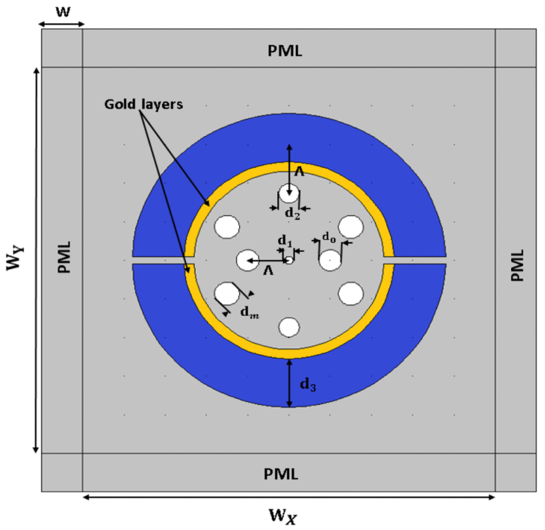
PhC and surface plasmon resonance (SPR) are two popular sensing technologies used in biochemical sensing. PhC structures utilize periodic nano-scale patterns to control the flow of light and create resonant modes that can be exploited to detect changes in the RI of the surrounding medium. SPR, conversely, uses the excitation of SPs on a thin metal film to measure changes in the RI near the surface of the film. Both PhC and SPR have benefits and limitations, and the selection of technology depends on the definite application needs. A unique PhC optical fiber biosensor utilizing the SPR principle is introduced, which provides a sensitivity level of 1000 nm/RIU [89]. PhC fiber (PhCF) is widely utilized for sensor design due to its unique structural features and properties. The structural parameters of PhCF can undoubtedly be modified as per the specific requirements of the sensor, which was previously difficult to achieve. Additionally, PhCF has a prominent level of birefringence, which enables it to distinguish between different polarizations of light. This makes it useful for sensors that detect changes in the polarization state of light. PhCF also has a high power fraction, which allows it to efficiently capture light and transmit it to the sensor. Furthermore, PhCF exhibits chromatic dispersion, which is useful for sensors that measure changes in the wavelength of light. Finally, PhCF has WG dispersion, which enables it to guide light along its length, making it useful for sensors that require light to be transmitted over a certain distance. These benefits make PhCF a smart option for sensor design. Researchers in [90] present an investigation into the computational analysis of a birefringent PhCF biosensor developed using the SPR model. Circular air holes, as shown in Figure 5, are used in a birefringent PhCF biosensor to allow multiple detections using and modes. A numerical analysis of the biosensor is conducted in amplitude and wavelength interrogation modes, resulting in sensing device resolution values of 5 × 10⁻⁵ RIU and 6 × 10⁻⁵ RIU for and modes, respectively, for spectral interrogation. For amplitude interrogation, the values are 3 × 10⁻⁵ RIU for modes and 4 × 10⁻⁵ RIU for modes. The PhCF biosensor exhibits the potential for multiple analyte detection with high sensitivity [90].
Fibre Bragg Gratings (FBGs) are optical devices that consist of a periodic variation in the RI of a fiber. This periodic variation acts as a wavelength-selective mirror, reflecting a specific wavelength of light while transmitting others. The spacing and depth of the periodic variation determine the wavelength of light that is reflected, making FBGs useful for filtering and sensing applications. FBGs are important optical devices due to their ability to measure physical parameters accurately and reliably, their ability to multiplex in a single fiber optic, their high stability in harsh environments, their small size, and their use as wavelength-selective filters in optical communication systems. Researchers developed a structural health monitoring system for aircraft wings using an optical fiber grating sensing network and a three-dimensional position correction algorithm established on FBG array test data [91]. The study proposed two fitting algorithms (bitone and spline with linear interpolations) to improve the accuracy of deformation parameter measurement. The experimental results showed that the bitone and spline interpolation methods improved the measurement accuracy of the system, with a relative error lower than 4.96% and an absolute error within 0.014 mm [92]. The study concluded that the FBG array measurements using these methods improve the fitting reconstruction effect for the wing structure and stabilize the compensation effect. A recent study has described a hot-wire anemometer established on a cladding-etched FBG coated with a layer of silver film and heated by a 1480 nm laser diode, as shown in Figure 6, to measure airflow velocity [93]. The study found that the heating efficiency of the FBG hot wire was improved by 3.8 times in magnitude by etching the fiber cladding from 125 μm down to 73.4 μm [93]. The achieved sensitivities at different airflow velocities were significantly higher than those of the reference anemometer without cladding etching. The results show that using cladding-etched FBG can improve the sensitivity of FBG-based hot-wire anemometers significantly.
Interferometric optical fiber devices are important because they exploit the wave nature of light and its interference phenomena to measure physical quantities such as strain, temperature, and pressure. These devices split a single beam of light into two, recombine them, and analyze the resulting interference pattern to determine the physical quantity being measured. They are established on fibers, which are thin and flexible strands of glass or plastic that can transmit light over long distances without significant loss of signal. Applications of interferometric optical fiber devices are found in aerospace, civil engineering, and biomedical engineering. Examples include interferometric sensors, gyros, and Fabry-Perot interferometers. A high-resolution optical fiber temperature sensor system utilizing an air-filled Fabry–Pérot (FP) cavity is described [38]. A fused-silica tube, a single-mode fiber, and a side-hole fiber are used to create the FP cavity, and the pressure is regulated by passing air through the side-hole fiber. The sensor demonstrates high-resolution temperature measurement and good stability in thermal cycle testing, with a maximum testing temperature of 800 °C [91]. Researchers have proposed an optical fiber temperature and strain sensor using dual MZIs that were assembled by fusion splicing of two different fibers [94]. The two MZIs have different responses to temperature and strain, and simultaneous measurement of both was experimentally justified using resonant dips in the transmission spectrum. The proposed sensors had maximum temperature and strain sensitivities of 66.67 pm/°C and −2.0 pm/µε, respectively, and could discriminate temperatures and strains as low as 0.20 °C and 0.71 µε, and 0.33 °C and 0.69 µε, respectively [94]. The sensor has potential applications due to its ease of fabrication, low costs, and good resolution.
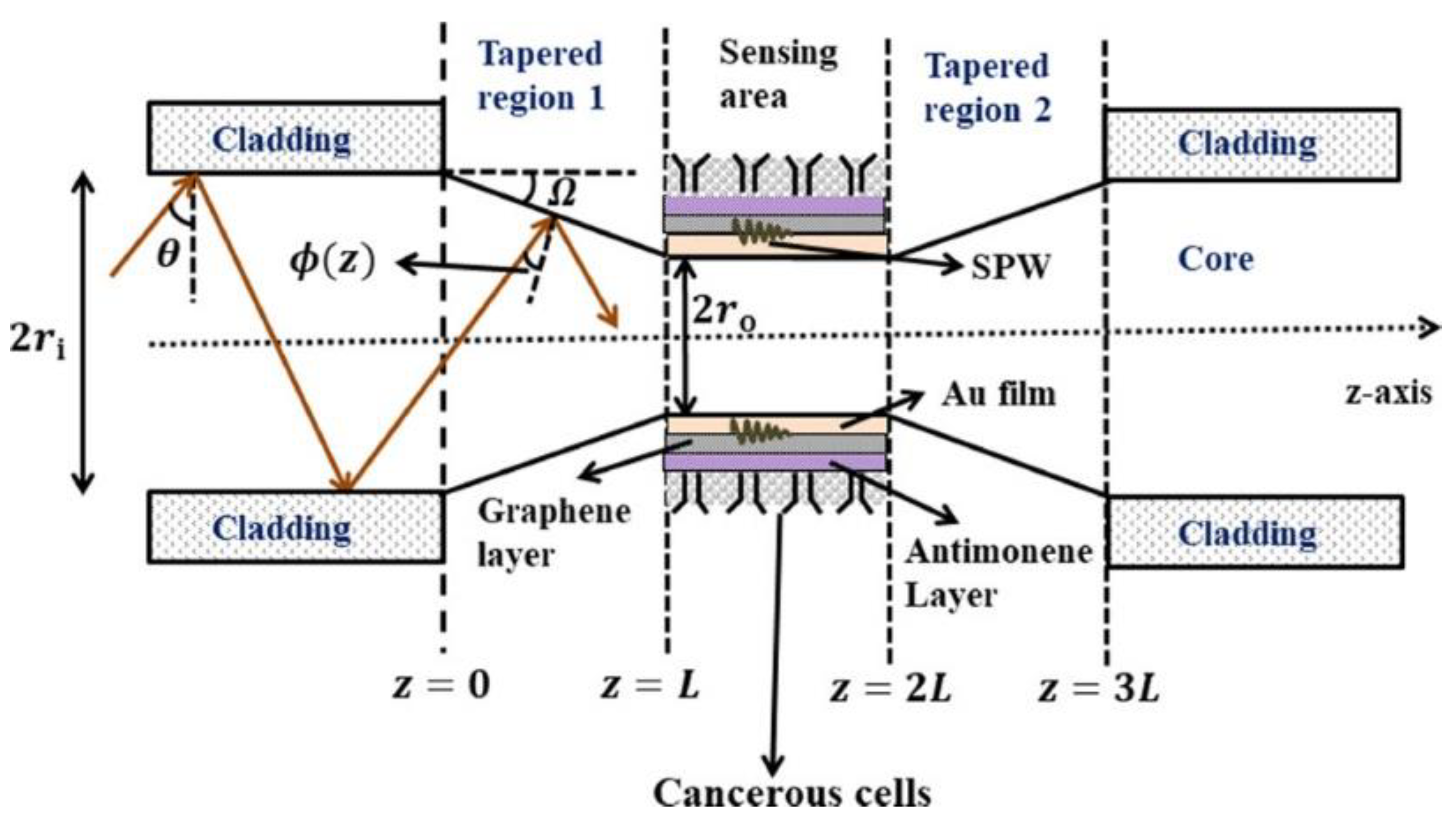
Surface Plasmon Resonance (SPR)-based fiber sensors can detect changes in the RI of a surrounding medium through the excitation of surface plasmon waves. They typically consist of a thin metal film deposited onto a fiber, and the sensitivity of the sensor is established by the distance between the metal film and the surrounding medium. When the RI of the surrounding medium changes, the metal film absorbs different wavelengths of light, resulting in a shift in the resonance angle that can be detected by a photodetector. These sensors are highly sensitive and have been used for a variety of applications, including biosensing, environmental monitoring, and chemical sensing. A team of researchers has demonstrated a new design of a graphene-antimonide-coated uniform-waist tapered fiber SPR biosensor, as shown in Figure 7, for early-stage cancer detection [95]. The biosensor has shown superior performance for early-stage cancer detection and can detect cancerous cells in the human body with refractive indices in the range of 1.36–1.4. The sensor’s design and analysis were conducted using a transfer matrix method-based simulation platform, and its performance was evaluated using various parameters. The numerical results showed that the SPR sensor has prospective applications in medical sciences for early-stage cancer diagnosis, with a maximum FOM of 131.1525 RIU−1, detection accuracy (DA) of 14.2126 μm−1, and LOD of 7.2 × 10⁻⁵ RIU [95].
Fluorescence-Based Fiber-Optic Probes (FF) are a type of sensor that detects changes in fluorescence signals through the excitation of fluorophores. They typically consist of an optical fiber and a fluorescent molecule attached to a sensing element. When excited by light, the fluorescent molecule emits light at a different wavelength, and the intensity of the emitted light is proportional to the concentration of the analyte being measured. FF probes are highly sensitive and have been used for a variety of applications, including environmental surveillance, medical diagnostics, and chemical sensing. Researchers developed a fluorescence-based fiber-optic temperature sensor by solidifying fluorescein and two of its derivatives, allyl fluorescein and diallyl fluorescein, in a GMA polymer matrix [96]. The sensitivity of the fluorescein dye to temperature changes was studied by investigating the two fluorescein derivatives separately, and their sensitivities were determined in different temperature ranges. The results showed that under room temperature, fluorescein dye in GMA polymer showed ineffective sensitivity to temperature changes. The fluorescence intensity peaks of allyl fluorescein dye in GMA polymer decreased slightly while warming up, while the fluorescence intensity peaks of diallyl fluorescein dye in GMA polymer showed a gradual decrease with sudden changes at specific temperatures. Above room temperature, the fluorescence intensity peaks decreased with rising temperature [96].
Light diffuser integrated optical fiber (LDOF) sensors are devices that use fibers with integrated light diffusers to measure physical constraints, for instance, temperature, pressure, and strain. These sensors can be used for several purposes, including structural health surveillance, biomedical sensing, and environmental surveillance. The light diffuser integrated into the fiber helps to distribute light uniformly over a sensing region, which improves the sensor’s sensitivity and accuracy. The sensors are also compact and can be easily integrated into existing systems, making them suitable for use in harsh environments or hard-to-reach places. Biocompatible materials were used to develop a photonic sensing platform to decrease the immune response in vivo in medical diagnostics. Real-time fiber sensors were created to measure stimuli-responsive polymers’ volumetric modulation using asymmetric microlens structures on stimuli-sensitive hydrogels [97]. These sensors were chemically attached to silica and biocompatible fibers, and a smartphone was used for quantitative measurements. To showcase the real-time sensing capabilities of the fiber probe, the researchers conducted experiments with different concentrations of ethanol, propanol, and dimethyl sulfoxide. They also observed that the fiber probe exhibited a quick response to changes in pH levels in the acidic region, with a sensitivity of 40 nW/pH. A microlens array-imprinted polymer was attached to a hydrogel fiber to develop biocompatible probes for physiological applications. In the reflection configuration, the fiber probe showed a sensitivity of 7 nW/pH [97]. These hydrogel fiber probes have potential applications in point-of-care diagnostics, continuous biomarker surveillance, and critical care sensing devices.
While fiber sensors offer numerous advantages, they also have some limitations and disadvantages. Optical fiber sensors can be more expensive compared to traditional sensors. The cost is primarily associated with the specialized fibers, connectors, and signal processing equipment required for their implementation. However, as technology continues to advance and become more widespread, the cost is gradually decreasing. Fibers are delicate and can be easily damaged. They are susceptible to bending, twisting, and mechanical stresses, which can lead to signal loss or complete failure. Care must be taken during installation and handling to ensure the integrity of the fibers. Installing fiber sensors can be more complex compared to traditional sensors. Proper alignment and connection of the fiber end, as well as ensuring the correct positioning and orientation of the sensing element, require skilled technicians and specialized equipment. Optical fibers have limitations on the maximum distance over which they can transmit light without significant signal loss. Attenuation, dispersion, and other factors can affect the signal quality and limit the range of the sensor. This can be addressed by using repeaters or signal amplifiers, but it adds complexity and cost to the system. Moreover, certain environmental conditions can impact the performance of optical fiber sensors. For example, high temperatures, extreme humidity, or exposure to certain chemicals may degrade the fiber or affect the accuracy of the measurements. Specialized fiber coatings or protective housing may be required in harsh environments. Optical fiber sensors can be influenced by external factors such as temperature fluctuations, vibrations, or EMI. These factors can introduce noise or affect the accuracy of the measurements. Appropriate calibration and compensation techniques may be necessary to mitigate these effects.
6. Optical WG-Based Sensing Devices
An optical WG is a physical structure that guides and confines EM waves, typically light, within a specific path or channel. These WGs are employed in a variety of applications, including telecommunications, medical equipment, and optical sensors [98]. Optical WGs can be made of various materials, such as glass, polymers, or semiconductor materials. The most common type of optical WG is a fiber cable, which uses a core made of glass or plastic to confine the light surrounded by a cladding layer that reflects the light into the core [99]. Other types of optical WGs include planar WGs, which are used in integrated optics, and PhC WGs, which use a periodic structure to confine the light [100].
Optical WG-based sensors are also extensively used in chemical and biological sensing applications [101,102,103], where they can detect changes in the surrounding environment with high sensitivity and specificity. These sensors, whether they are chemical, gas, or biosensors, all rely on the same basic principle. They use optical WGs to detect changes in the RI of the sample caused by the presence of the target molecule or gas. The specific type of optical WG-based sensor used depends on the type of molecule or gas being sensed. Regardless of the specific type of sensor used, optical WG-based sensors offer several advantages over other sensing technologies. They are sensitive, selective, and can detect extremely low concentrations of target molecules or gases. Optical WG-based sensors have several purposes in various fields, including environmental surveillance, biomedical research, clinical diagnostics, industrial process control, and safety and security [104]. They can be used to detect pollutants in water, gases in the atmosphere, biomolecules in biological samples, and toxic gases in industrial settings.
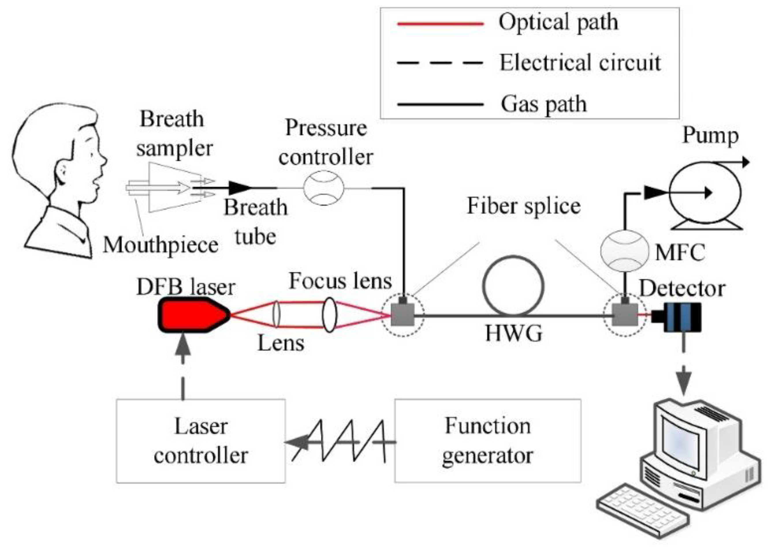
The analysis of breathing gases is a practical approach for the diagnosis of diseases or monitoring metabolic conditions. This diagnostic method offers the benefit of being non-invasive and extremely safe, mainly when compared to other diagnostic techniques. It can also easily obtain samples from individuals with serious illnesses, including elderly people or newborns. Furthermore, it provides doctors and patients with real-time results, which is particularly valuable for the early detection of diseases. The authors of the study [105], developed a mid-infrared gas sensor established on a hollow waveguide (HWG) and distributed feedback lasers as shown in Figure 8, which were able to instantaneously measure concentration changes of various isotopologues in exhaled breath and determine isotope ratios. The sensing system had a swift response time of 3 s and was found to be precise and accurate in measuring isotopic ratios. The use of Kalman filtering improved precision and accuracy even further. The sensor has the potential for respiratory surveillance and disease diagnosis.
Effective surveillance of air quality is essential due to the significant impact of air pollution on public health and the environment. The current traditional air quality surveillance methods are limited and expensive, making them less effective in providing comprehensive information. Hence, the development of smaller and more cost-effective devices can authorize widespread surveillance of air quality, letting policymakers and individuals make informed decisions to improve air quality. The advancement of a passively demodulated interferometer established on 3 × 3 WG couplers for measuring light absorption of trace gases and aerosol particles through the photothermal effect is presented [106]. This system does not require active quadrature control and uses an algorithm for evaluating the photothermal interferometry signal. NO2 calibration experiments are conducted using different couplers, and the results of a laboratory measurement campaign using aerosolized nigrosin are conferred. The article highlights interferometer phase noise as the primary noise component and recommends improving the setup to improve the current instrumental detection limit, which is currently at a value of 100 Mm−1 (1σ, 60 s), corresponding to mass concentrations of about 10 µg/m3 for submicrometer-size black carbon particles.
PCB-integrated optical WG sensors are a type of sensing technology that combines printed circuit board (PCB) technology with optical WGs to create high-performance, low-cost sensing devices. The integration of PCB technology and optical WGs allows for the shrinking of the sensing device and enables the creation of large-scale sensor arrays, making it possible to monitor multiple parameters simultaneously. This technology has numerous applications, including environmental surveillance, medical diagnostics, and industrial process control. Recently, a study [107] presented a new platform for cost-effective PCB-integrated optical WG sensors that use polymer WGs and commercial chemical dyes. The study demonstrates the fabrication and assembly of a PCB-integrated ammonia gas sensor, achieving a sensitivity of approximately 30 ppm and a linear response of up to 600 ppm at room temperature. The capability of detecting multiple analytes from a single device via principal-component analysis is also demonstrated.
Researchers have investigated optical fiber- or WG-based pH sensors over the past two decades to improve their sensitivity and miniaturization. A recent study [108] proposes a new and economical pH sensor based on polymer WG Bragg grating, as shown in Figure 9, that addresses crucial aspects such as sensitivity enhancement, miniaturization, narrow band response, and stable performance. The proposed sensor realized a sensitivity of 10.4 nm/pH for a pH range of 4 to 7, which is two orders higher than all other Bragg grating pH sensors. It also has a narrow band response and excellent fabrication tolerances, making it suitable for the perishable food industry.
Currently, there is a high demand for biosensor technologies that can rapidly and inexpensively detect a variety of contaminants in water. WG-based evanescent wave fluorescent biosensors have gained significant attention due to their high sensitivity, selectivity, and potential for easy miniaturization. A fluorescent immunosensor capable of detecting up to 32 contaminants rapidly and simultaneously has been developed using an integrated channel WG [109]. WG tapers enhance the efficiency of excitation and collection of fluorescent signals in the presence of fluorophore photobleaching in a solid-surface bioassay. The immunosensor is the first of its kind for detecting microcystin-LR (MC-LR) in lake water using an adjusted WG geometry. All real lake samples, including those containing MC-LR in the sub-microgram per liter range, could be verified with recovery rates between 84% and 108%, indicating its capability to measure MC-LR in water samples [109].
Optical WG sensors typically have a limited range of operation. The sensing range is determined by the length of the WG, and it may not be suitable for applications that require long-distance measurements. WG sensors often require specific types of WGs that are designed for a particular wavelength or range of wavelengths. This can limit their compatibility with different sensing applications, especially if the desired wavelength is outside the range supported by the structure.
The fabrication and installation of optical WG sensors can be complex and require specialized equipment and expertise. This can increase the cost and complexity of implementing these sensors, especially for large-scale applications. Furthermore, optical WG sensors are typically made of delicate materials, such as glass, polymers, or semiconductors, which can be susceptible to physical damage [14]. Any damage to the WG can affect the sensor’s performance and require costly repairs or replacements. Optical WG sensors can be more expensive compared to other sensing technologies, especially for customized or specialized applications [110]. The cost of the WG materials, fabrication processes, and supporting equipment can contribute to the overall expense. However, it is important to note that the specific disadvantages of optical WG sensors can vary depending on the design, implementation, and intended application. Some of these limitations can be addressed through ongoing research and development efforts in the field.
7. Optical Wearable Sensors
In a short period of time, wearable sensing technology has transformed from a science fiction idea to a wide variety of practical consumer and medical gadgets [111]. Wearable sensors consist of a sensing element that interacts with the physical quantity being measured. The sensing element can be based on various principles, such as piezoelectric, capacitive, resistive, optical, or magnetic. The specific design of the sensing element depends on the type of sensor and the target application. It is important to note that the sensitivity of wearable sensors can vary depending on factors such as the sensor design, manufacturing quality, environmental conditions, and specific application requirements. Different sensors may have different sensitivity levels, and choosing the appropriate sensor for a particular application involves considering factors like the desired measurement range, resolution, and nature of the physical quantity being measured. Wearables are growing because of factors including the accessibility and user-friendliness of miniaturized electronics, the emergence of smartphones and other connected devices, the growing consumer demand for health awareness, and the unfulfilled need for doctors to continuously collect high-quality medical data from their patients [112]. Amid growing achievements, there is always a desire for additional information from the body. Due to the non-specific nature of most sensing modalities used in contemporary wearables (pulse, galvanic skin reaction, etc.), this demand is still unfulfilled (e.g., how many factors can increase your pulse or trigger you to sweat). Furthermore, most wearable sensing devices employ methods that have been in use for many years. Even the most complicated wearables, such as continuous transdermal glucose monitors, profit from nearly 30 years of improvements in enzyme electrodes found in basic and incredibly affordable finger-prick glucose test strips. In addition, transdermal glucose measurement may be the only commonly used wearable that continually tracks the progress of a severe ailment [113,114].
The global wearable sensing market is anticipated to be worth $5.5 billion by 2025, with presently under-development technologies making up approximately a third of that sum [115]. A wearable sensing device, such as a customized fitness surveillance device, is currently owned by over 1/10 of Americans, a threefold increase from 2012 [116]. By collecting data on the pulse, blood oxygen level, motion, movement, step count, and even eating and sleeping behaviors via mobile phones and cloud connections, fitness trackers and smartwatches may develop tailored health profiles [117]. Non-intrusive biomedical measurements are frequently carried out optically, with the area of the skin that must be evaluated exposed to a light source of a certain wavelength [118]. The sensing device collects light that is refracted, reflected, and absorbed. It then describes and quantifies the biological data (the identical sensations as employed by the spectrophotometer). The most crucial element for sending an optical signal via the skin is that it determines how far the light may go. These light beams can vary from UV to deep IR, according to the necessary penetration depth and significant absorption peak for the appropriate sensing application. Figure 10 shows the upsurge of wearable sensing devices and the future of wearable technology [119].
Wearable optical heart rate monitors (HRMs) established on PPG have become incredibly popular, with a plethora of tech companies creating and promoting them [120,121]. Many companies, including Sony, Microsoft, Apple, Motorola, FitBit, MioGlobal, and Masimo, have created optical PPG sensing devices that may be placed on the wrist, around the chest, or even in the ears, utilizing optical sensing devices focusing on headphones that work in the reflection mode. Due to their compact size and ability to create stronger signals via transmission-based readings because of their placement on the finger, ring PPG devices are also of concern. Nowadays, a variety of optical and electrical activities may be completed by currently on-the-market sensing devices, such as monitoring blood oxygen levels and PPGs for pulse tracking, counting steps, breathing rates, body temperatures, and even determining sleep quality [122]. Sportspeople are always searching for new treatments and technology to enhance their abilities and stay healthy [123]. More and more athletes are using wearables to monitor their training and recovery. The inside and outside workloads of athletes are currently tracked by sports teams using wearable technology. The next technological gap for sports medicine practitioners to tailor hydration and recovery plans to each athlete is the ability to continuously monitor indicators from saliva or sweat unobtrusively [124]. Over the past two decades, wearable sensing devices have changed from being seen from a device viewpoint to a strategic perspective, with the system merging the device with data. There remains a medical need to assess, establish, and confirm this automation, especially for sports medicine. An earlier study has focused on specific technical domains of the wearables field, such as smart sensors [125,126], materials [127,128], and soft interfaces [129], or on the manufacturing and use of such gadgets to concentrate on health conditions such as atrial fibrillation [130], cystic fibrosis [131], or diabetes [132,133]. There is still an unfulfilled need to evaluate, establish, and assure this technology, particularly for sports medicine [134].
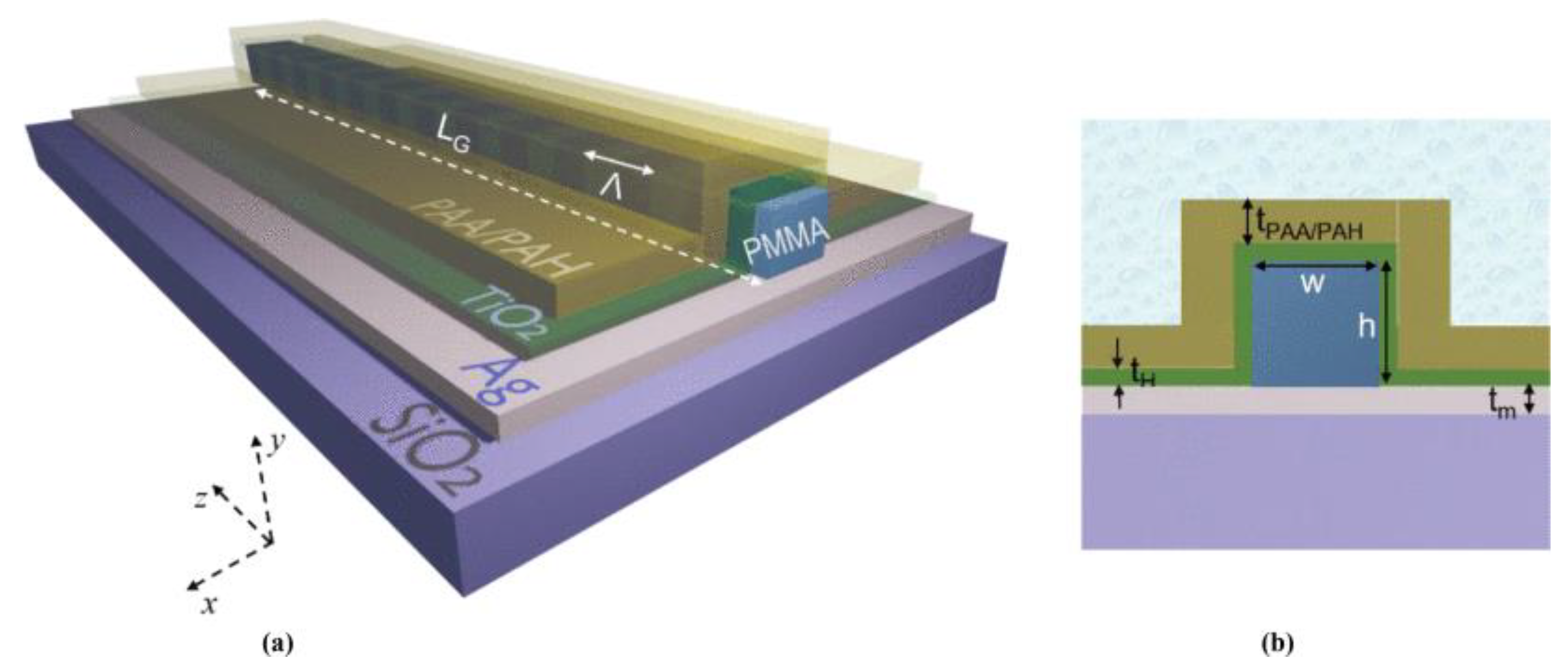
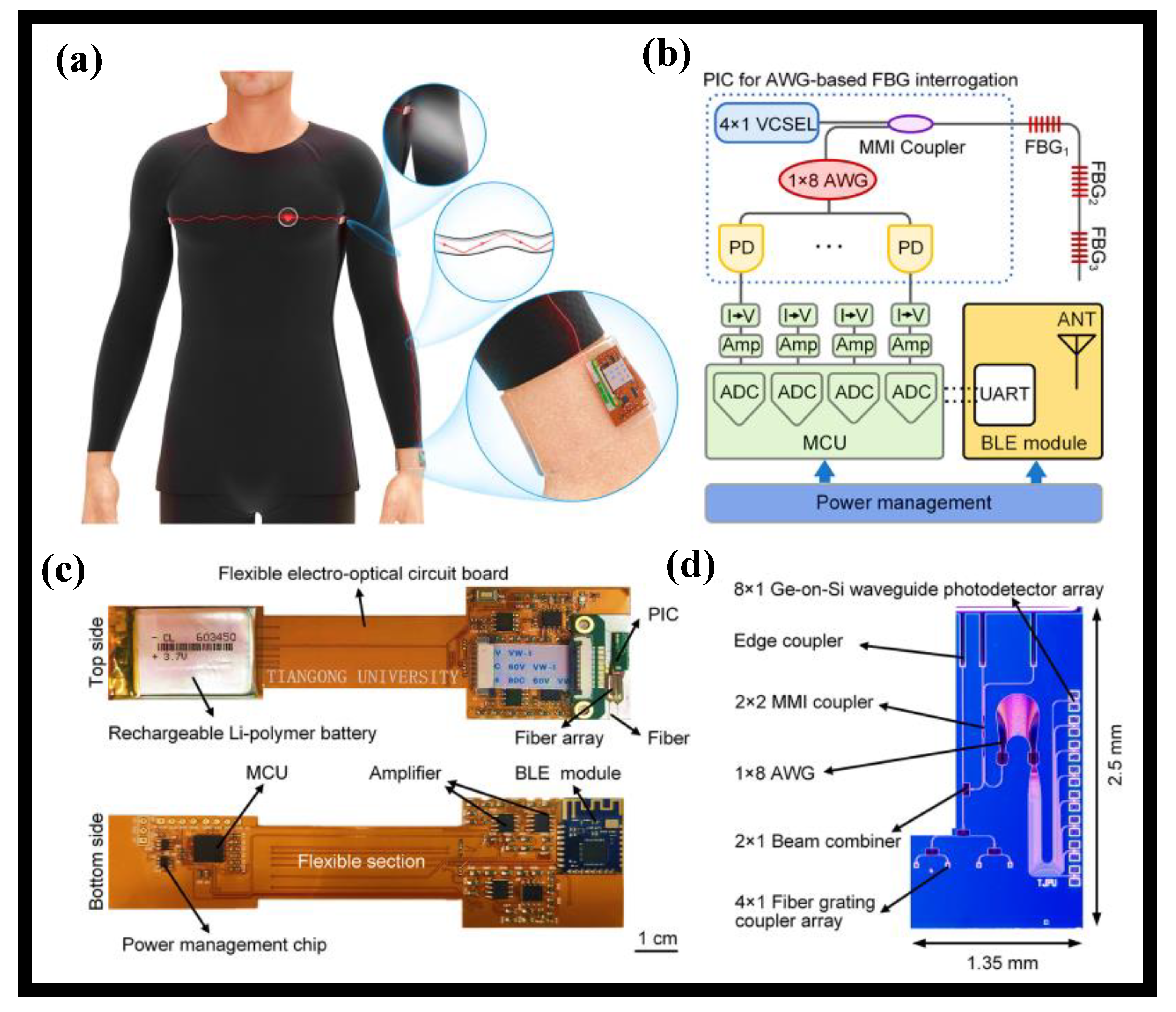
For enhanced multiparameter sensing in digital health monitoring systems, wearable sensors are the most advantageous. The first demonstration of a completely integrated optical interrogator is made [135]. For the continuous, dynamic, and long-term capture of human physiological data, an optical interrogator that is robust, compact, and inexpensive is produced by consolidating all the optical components on a silicon photonic chip. The interrogator was built inside a bracelet, making it possible to monitor heartbeats and measure body temperature. Figure 11a shows how the wearable flexible integrated optical integrator (WFIOI) is primarily made up of three FBGs placed on skin-tight garments and a flexible electro-optical circuit board with a wristband construction. A schematic of the fully flexible electro-optical circuit and the manufactured circuit board is shown in Figure 11b,c, respectively. Figure 11d shows the PIC’s conceptual architecture. A 4 × 1 long-wavelength VCSEL array, a 1 × 8 AWG edge coupler, a 2 × 2 MMI coupler, a 2 × 1 combiner, a 4 × 1 fiber grating coupler array, an integrated 8-channel Ge-on-Si WG PD array, straight WGs, and bend WGs were all included in the PIC, which had a size of roughly 2.5 mm 1.35 mm. The light source array is made up of four VCSELs with center wavelengths of 1545.34, 1548.53, 1551.33, and 1552.15 nm [135]. The findings of this work may be immediately used in the specialized design of ultra-downsized optical interrogator systems and open the way for the creation of integrated wearable optical interrogators the size of watches that may find use in health monitoring.
8. Current Challenges Associated with the Development of Photonic Sensors
There are particular difficulties in the development of photonic sensors. Realizing high sensitivity in photonic sensors is one of the main difficulties. The degree of a sensor’s sensitivity affects its capacity to identify minute variations in the quantity being measured. It takes careful consideration and optimization to create sensors that can pick up on really low light levels or minute changes in other optical characteristics [5].
Thermal noise, shot noise, and electronic noise are only a few of the several types of noise that photonic sensors are particularly vulnerable to [136]. These noise sources have the potential to reduce the sensor’s overall performance and lower the signal-to-noise ratio. Continuous difficulties in the development of photonic sensors include lowering noise levels and enhancing signal processing methods. Additionally, there are many environmental conditions that might affect the performance of photonic sensors. For instance, changes in temperature, humidity, vibrations, electromagnetic interference, and ambient light can have an impact on how accurately and consistently the sensor measures various conditions. It is essential to create plans to reduce or make up for these environmental consequences.
Fabricating and integrating photonic sensors with other components or systems can be complex. Photonic sensors often require precise fabrication processes, including lithography, etching, and deposition techniques [137]. Integration with other components, such as light sources, detectors, and electronics, poses additional challenges to ensure compatibility and optimal performance. In many applications, there is a need for miniaturized photonic sensors that can be integrated into compact devices or deployed in challenging environments. Miniaturization brings challenges in terms of maintaining or improving sensor performance while reducing size and power consumption.
Cost is a significant consideration in the development and deployment of photonic sensors. Certain fabrication techniques and materials used in photonic sensor technologies can be expensive, limiting their widespread adoption. Finding cost-effective manufacturing processes and scalable production methods is an ongoing challenge [138].
Photonic sensors often require calibration to maintain accurate and reliable measurements. Factors such as aging effects, drift, and variations in environmental conditions can impact the sensor’s calibration and long-term stability. Developing robust calibration methods and ensuring sensor stability over extended periods are essential challenges [139].
Interdisciplinary initiatives integrating materials science, optics, electronics, signal processing, and system integration are necessary to meet these problems. To conquer these obstacles and realize the full potential of photonic sensors in a variety of applications, including biological sensing, environmental monitoring, telecommunications, and industrial ones, more research and technological improvements are required.
9. Concluding Remarks
Photonic sensors have seen substantial advances in recent years, driven by the increasing demand for high-precision and high-sensing technologies in a wide range of applications, including environmental surveillance, medical diagnostics, and industrial automation [42]. The integration of photonic sensors with microelectronics has led to the advancement of compact and low-priced sensors that can be easily integrated with other electronic systems. This has opened new applications in areas such as healthcare, where integrated sensing devices can be utilized for real-time monitoring of vital signs. Optical fiber-based sensors use optical fibers to detect changes in temperature, pressure, or strain. These sensors offer several benefits over traditional electronic sensors, including higher sensitivity, resistance to electromagnetic obstruction, and the ability to function in harsh environments. Recently, SPR-based sensors emerged as a promising platform for sensing applications that use the interaction between light and metallic nanostructures to perceive shifts in the RI of the ambient medium. These sensors offer high sensitivity and can be engaged for label-free recognition of biomolecules and other analytes [45]. Moreover, photonic crystal-based sensors use variations in the properties of the photonic crystal to detect changes in the surrounding environment. These sensors offer high sensitivity and can be exploited for applications such as chemical sensing and biosensing. Plasmonic sensors can also be utilized to detect and monitor various types of pollutants in the environment, including heavy metals, organic compounds, and gases. The high sensitivity and label-free detection capabilities of plasmonic sensors make them well-suited for real-time monitoring of pollutant concentrations in air, water, and soil [140]. They can be employed for the assessment of water quality parameters such as pH, salinity, dissolved oxygen, and turbidity. By functionalizing the plasmonic structures with specific receptors or indicators, changes in these parameters can be detected and quantified. Plasmonic sensors can enable rapid and portable water quality analysis, which is crucial for environmental conservation and human health.
Medical optical sensors may perform a wide range of tasks [25]. They may be employed to enhance the intelligence of medical devices and implants, as well as to continuously monitor human physiology even when the patient is not present. Monitoring bodily functions makes it simpler to identify vital signals like heart rate, respiration rate, blood pressure, etc., enabling early, speedy diagnosis and prevention [26,114]. It also helps patients keep track of their physiological parameters and notify their doctor if something changes. The form factors of most of the commercially accessible wearable technology are ultimately confined by the size and weight of the batteries needed for the power supply, which are mechanically hard components linked to bands and worn on the wrist. Many pieces of health information are contained in basic physiological signals. By analyzing the pulsatile constituent of the bloodstream, it is feasible to estimate important physiological parameters such as pulse inconstancy or variability employing photoplethysmography (PPG) and oxygen saturation in arterial blood using pulse oximetry [120,121]. A new kind of automation called wearable devices with “skin-like” properties is only now beginning to leave R&D laboratories and enter pre-commercial models. Due to their deformability, lightness, mobility, and flexibility, flexible skin-like sensors have reached various capabilities that were previously unattainable for conventional sensing devices [112].
Author Contributions
Conceptualization, M.A.B. and M.S.; methodology, M.A.B.; software, M.A.B.; validation, M.A.B.; formal analysis, M.A.B.; investigation, M.A.B.; resources, M.A.B.; data curation, M.S. and M.A.B.; writing—original draft preparation, M.S. and M.A.B.; writing—review and editing, M.A.B. and R.P.; visualization, M.A.B. and R.P.; supervision, M.A.B. and R.P.; project administration, M.S. and M.A.B.; funding acquisition, M.A.B. All authors have read and agreed to the published version of the manuscript.
Funding
This research received no external funding.
Institutional Review Board Statement
Not applicable.
Informed Consent Statement
Not applicable.
Data Availability Statement
Not applicable.
Acknowledgments
The author acknowledges the support from the Warsaw University of Technology for the completion of this work.
Conflicts of Interest
The authors declare no conflict of interest. The funders had no role in the design of the study; in the collection, analyses, or interpretation of data; in the writing of the manuscript; or in the decision to publish the results.
Abbreviations
Photonic integrated circuit—PIC; Waveguide—WG; Photonic crystal—PhC; Photonic crystal fiber—PhCF; Surface plasmon resonance—SPR; Metal-insulator-metal—MIM; Photoplethysmography—PPG; Localized surface plasmon polariton—LSPR; Surface plasmon—SP; Photonic crystal enhanced microscopy—PhCEM; Refractive index—RI; Internet of Things—IoT; Electromagnetic interference—EMI; Finite difference time domain—FDTD; Limit of detection—LoD; Mach–Zehnder interferometer—MZI; Figure of merit—FOM; Electron-beam lithography—EBL; Nanoimprint lithography—NIL; Propagating surface plasmon polariton—PSPP; Surface-enhanced Raman spectroscopy—SERS; Black phosphorous—BP; Near-infrared—NIR; Electron-beam lithography—EBL; Focused ion beam—FIB; Volatile organic compound—VOC; Total internal reflection—TIR; Fiber Bragg Grating—FBG; Fabry–Pérot—FP; Fluorescence-Based Fiber-Optic—FF; Light diffuser integrated optical fiber—LDOF; Hollow waveguide—HWG; Electromagnetic—EM; Printed circuit board—PCB; Ultraviolet—UV; Infrared—IR; Heart rate monitors—HRM; Wearable flexible integrated optical integrator—WFIOI.
References
- Chen, S.; Wang, J.; Zhang, C.; Li, M.; Li, N.; Wu, H.; Liu, Y.; Peng, W.; Song, Y. Marine Structural Health Monitoring with Optical Fiber Sensors: A Review. Sensors 2023, 23, 1877. [Google Scholar] [CrossRef]
- Ferreira, P.M.; Machado, M.A.; Carvalho, M.S.; Vidal, C. Embedded Sensors for Structural Health Monitoring: Methodologies and Applications Review. Sensors 2022, 22, 8320. [Google Scholar] [CrossRef]
- Krivosheev, A.I.; Barkov, F.L.; Konstantinov, Y.A.; Belokrylov, M.E. State-of-the-Art Methods for Determining the Frequency Shift of Brillouin Scattering in Fiber-Optic Metrology and Sensing (Review). Instrum. Exp. Tech. 2022, 65, 687–710. [Google Scholar] [CrossRef]
- Lu, P.; Lalam, N.; Badar, M.; Liu, B.; Chorpening, B.T.; Buric, M.P.; Ohodnicki, P.R. Distributed optical fiber sensing: Review and perspective. Appl. Phys. Rev. 2019, 6, 041302. [Google Scholar] [CrossRef]
- Butt, M.; Voronkov, G.; Grakhova, E.; Kutluyarov, R.; Kazanskiy, N.; Khonina, S. Environmental Monitoring: A Compre-hensive Review on Optical Waveguide and Fiber-Based Sensors. Biosensors 2022, 12, 1038. [Google Scholar] [CrossRef]
- Arano-Martinez, J.; Martinez-Gonzalez, C.; Salazar, M.; Torres-Torres, C. A framework for biosensors assisted by mul-tiphoton effects and machine learning. Biosensors 2022, 12, 710. [Google Scholar] [CrossRef]
- Kazanskiy, N.L.; Khonina, S.N.; Butt, M.A. Recent Development in Metasurfaces: A Focus on Sensing Applications. Nanomaterials 2022, 13, 118. [Google Scholar] [CrossRef]
- Irfan, M.; Khan, Y.; Rehman, A.U.; Butt, M.A.; Khonina, S.N.; Kazanskiy, N.L. Plasmonic Refractive Index and Temperature Sensor Based on Graphene and LiNbO3. Sensors 2022, 22, 7790. [Google Scholar] [CrossRef]
- Daher, M.G.; Taya, S.A.; Colak, I.; Vigneswaran, D.; Olaimat, M.M.; Patel, S.K.; Ramahi, O.M.; Almawgani, A.H. Design of a nano-sensor for cancer cell detection based on a ternary photonic crystal with high sensitivity and low detection limit. Chin. J. Phys. 2022, 77, 1168–1181. [Google Scholar] [CrossRef]
- Wu, R.; Biondi, A.; Cao, L.; Gandhi, H.; Abedin, S.; Cui, G.; Yu, T.; Wang, X. Composite Bridge Girders Structure Health Monitoring Based on the Distributed Fiber Sensing Textile. Sensors 2023, 23, 4856. [Google Scholar] [CrossRef]
- Nowak, S.; Sherizadeh, T.; Esmaeelpour, M.; Guner, D.; Karadeniz, K.E. Hybrid Fiber Optic Cable for Strain Profiling and Crack Growth Measurement in Rock, Cement, and Brittle Installation Media. Sensors 2022, 22, 9685. [Google Scholar] [CrossRef] [PubMed]
- Yuan, B.; Ying, Y.; Morgese, M.; Ansari, F. Theoretical and Experimental Studies of Micro-Surface Crack Detections Based on BOTDA. Sensors 2022, 22, 3529. [Google Scholar] [CrossRef] [PubMed]
- Png, W.H.; Lin, H.S.; Pua, C.H.; Abd Rahman, F. Pipeline monitoring and leak detection using Loop integrated Mach Zehnder Inter-ferometer optical fiber sensor. Opt. Fiber Technol. 2018, 46, 221–225. [Google Scholar] [CrossRef]
- Khonina, S.; Voronkov, G.; Grakhova, E.; Kazanskiy, N.; Kutluyarov, R.; Butt, M. Polymer Waveguide-Based Optical Sen-sors—Interest in Bio, Gas, Temperature, and Mechanical Sensing Applications. Coatings 2023, 13, 549. [Google Scholar] [CrossRef]
- Zhirnov, A.A.; Chesnokov, G.Y.; Stepanov, K.V.; Gritsenko, T.V.; Khan, R.I.; Koshelev, K.I.; Chernutsky, A.O.; Svelto, C.; Pnev, A.B.; Valba, O.V. Fiber-Optic Telecommunication Network Wells Monitoring by Phase-Sensitive Optical Time-Domain Reflectometer with Disturbance Recognition. Sensors 2023, 23, 4978. [Google Scholar] [CrossRef]
- Zahir, M.H.M.; Aziz, K.M.A.; Ghazali, A.R.; Latiff, A.H.A. Effectiveness of Fiber Optic Distributed Acoustic Sensing (DAS) in Vertical Seismic Profiling (VSP) Field Survey. Appl. Sci. 2023, 13, 5002. [Google Scholar] [CrossRef]
- Weiss, M.; Srivastava, R.; Groger, H.; Lo, P.; Luo, S.-F. A theoretical investigation of environmental monitoring using sur-face plasmon resonance waveguide sensors. Sens. Actuators A Phys. 1996, 51, 211–217. [Google Scholar] [CrossRef]
- Kazanskiy, N.; Khonina, S.; Butt, M. Polarization-insensitive hybrid plasmonic waveguide design for evanescent field ab-sorption gas sensor. Photonic Sens. 2021, 11, 279–290. [Google Scholar] [CrossRef]
- Butt, M.A. Numerical Assessment of a Metal-Insulator-Metal Waveguide-Based Plasmonic Sensor System for the Recognition of Tuberculosis in Blood Plasma. Micromachines 2023, 14, 729. [Google Scholar] [CrossRef]
- Ali, S.; Khan, S.; Bermak, A. Inkjet-Printed Human Body Temperature Sensor for Wearable Electronics. IEEE Access 2019, 7, 163981–163987. [Google Scholar] [CrossRef]
- Asada, H.; Shaltis, P.; Reisner, A.; Rhee, S.; Hutchinson, R. Mobile monitoring with wearable photoplethysmographic bio-sensors. IEEE Eng. Med. 2003, 22, 28–40. [Google Scholar] [CrossRef] [PubMed] [Green Version]
- Bent, B.; Goldstein, B.A.; Kibbe, W.A.; Dunn, J.P. Investigating sources of inaccuracy in wearable optical heart rate sensors. NPJ Digit. Med. 2020, 3, 18. [Google Scholar] [CrossRef] [PubMed] [Green Version]
- Colella, R.; Catarinucci, L. 3D printed wearable sensor tag based on UHF RFID ICs implementing a novel interrogation modality. In Proceedings of the International Conference on IC Design & Technology (ICICDT), Otranto, Italy, 4–6 June 2018; pp. 17–20. [Google Scholar]
- Liu, J.; Liu, M.; Bai, Y.; Zhang, J.; Liu, H.; Zhu, W. Recent Progress in Flexible Wearable Sensors for Vital Sign Monitoring. Sensors 2020, 20, 4009. [Google Scholar] [CrossRef] [PubMed]
- Kazanskiy, N.L.; Butt, M.A.; Khonina, S.N. Recent advances in wearable optical sensor automation powered by battery versus skin-like battery-free devices for personal healthcare—A review. Nanomaterials 2022, 12, 334. [Google Scholar] [CrossRef]
- Butt, M.A.; Kazanskiy, N.L.; Khonina, S.N. Revolution in Flexible Wearable Electronics for Temperature and Pressure Monitoring—A Review. Electronics 2022, 11, 716. [Google Scholar] [CrossRef]
- Bayoumy, K.; Gaber, M.; Elshafeey, A.; Mhaimeed, O.; Dineen, E.H.; Marvel, F.A.; Martin, S.S.; Muse, E.D.; Turakhia, M.P.; Tarakji, K.G.; et al. Smart wearable devices in cardiovascular care: Where we are and how to move forward. Nat. Rev. Cardiol. 2021, 18, 581–599. [Google Scholar] [CrossRef]
- Francoeur, J.; Roberge, A.; Lorre, P.; Monet, F.; Wright, C.; Kadoury, S.; Kashyap, R. Optical frequency domain reflectometry shape sensing using an extruded optical fiber triplet for intra-arterial guidance. Opt. Express 2023, 31, 396–410. [Google Scholar] [CrossRef]
- Monet, F.; Sefati, S.; Lorre, P.; Poiffaut, A.; Kadoury, S.; Armand, M.; Iordachita, I.; Kashyap, R. High-Resolution Optical Fiber Shape Sensing of Continuum Robots: A Comparative Study. In Proceedings of the 2020 IEEE International Conference on Robotics and Automation (ICRA), Paris, France, 15 September 2020. [Google Scholar]
- Islam, F.; Wanigasekara, C.; Rajan, G.; Swain, A.; Prusty, B.G. An approach for process optimisation of the Automated Fibre Placement (AFP) based thermoplastic composites manufacturing using Machine Learning, photonic sensing and thermo-mechanics modelling. Manuf. Lett. 2022, 32, 10–14. [Google Scholar] [CrossRef]
- Rogers, C.; Piggott, A.Y.; Thomson, D.J.; Wiser, R.F.; Opris, I.E.; Fortune, S.A.; Compston, A.J.; Gondarenko, A.; Meng, F.; Chen, X.; et al. A universal 3D imaging sensor on a silicon photonics platform. Nature 2021, 590, 256–261. [Google Scholar] [CrossRef]
- Available online: https://www.futuremarketinsights.com/reports/photonics-sensor-and-detector-market (accessed on 10 June 2023).
- Arthurs, E.G. Perspectives on the future of photonics: The best is yet to come. Adv. Photon. 2019, 1, 010501. [Google Scholar] [CrossRef] [Green Version]
- Butt, M.; Khonina, S.; Kazanskiy, N. 2D-Photonic crystal heterostructures for the realization of compact photonic devices. Photonics Nanostruct.-Fundam. Appl. 2021, 44, 100903. [Google Scholar] [CrossRef]
- Butt, M.; Khonina, S.; Kazanskiy, N. Recent advances in photonic crystal optical devices: A review. Opt. Laser Technol. 2021, 142, 107265. [Google Scholar] [CrossRef]
- Yang, D.; Wang, X.; Tian, H.; Ji, Y. Electro-optic modulation property of slow light in coupled photonic crystal resonator arrays. Opt. Appl. 2011, 41, 753–763. [Google Scholar]
- Chen, Y.; Dong, J.; Liu, T.; Zhu, Q.; Chen, W. Refractive index sensing performance analysis of photonic crystal containing graphene based on optical Tamm state. Mod. Phys. Lett. B 2016, 30, 1650030. [Google Scholar] [CrossRef]
- Poonguzhali, S.; Sivasangari, A.; Ajitha, P.; Lalithakumari, S.; Sridevi, A.; Danasegaran, S.K. Design and performance analysis of smart photonic sensors for industrial applications. Curr. Appl. Phys. 2022, 39, 183–189. [Google Scholar]
- Rodriguez, G.A.; Markov, P.; Cartwright, A.P.; Choudhury, M.H.; Afzal, F.O.; Cao, T.; Halimi, S.I.; Retterer, S.T.; Kravchenko, I.I.; Weiss, S.M. Photonic crystal nanobeam biosensors based on porous silicon. Opt. Express 2019, 27, 9536–9549. [Google Scholar] [CrossRef]
- Fan, S.; Joannopoulos, J.D. Analysis of guided resonances in photonic crystal slabs. Phys. Rev. B 2002, 65, 235112. [Google Scholar] [CrossRef] [Green Version]
- Khani, S.; Hayati, M. Optical biosensors using plasmonic and photonic crystal band-gap structures for the detection of basal cell cancer. Sci. Rep. 2022, 12, 5246. [Google Scholar] [CrossRef]
- Chen, W.; Long, K.; Lu, M.; Chaudhery, V.; Yu, H.; Choi, J. Photonic crystal enhanced microscopy for imaging of live cell adhesion. Analyst 2013, 138, 5886–5894. [Google Scholar] [CrossRef]
- Zhou, Y.; Hu, H.; Chen, W.; Lu, M.; Tian, L.; Yu, H. Single nanoparticle detection using photonic crystal enhanced micros-copy. Analyst 2014, 139, 1007–1015. [Google Scholar] [CrossRef]
- Scullion, M.; Falco, D.; Krauss, T. Slotted photonic crystal cavities with integrated microfludics for biosensing applications. Biosens. Bioelectron. 2011, 27, 101–105. [Google Scholar] [CrossRef] [PubMed]
- Kazanskiy, N.; Khonina, S.; Butt, M. Plasmonic sensors based on Metal-insulator-metal waveguides for refractive index sensing applications: A brief review. Phys. E Low-Dimens. Syst. Nanostruct. 2019, 117, 113798. [Google Scholar] [CrossRef]
- Kamada, S.; Okamoto, T.; El-Zohary, S.E.; Haraguchi, M. Design optimization and fabrication of Mach-Zehnder interfer-ometer based on MIM plasmonic waveguides. Optics Express 2016, 24, 16224–16231. [Google Scholar] [CrossRef] [PubMed]
- Guan, X.; Wang, X.; Frandsen, L.H. Optical temperature sensor with enhanced sensitivity by employing hybrid waveguides in a silicon Mach-Zehnder interferometer. Opt. Express 2016, 24, 16349–16356. [Google Scholar] [CrossRef] [PubMed] [Green Version]
- Martínez, A.; Sanchis, P.; Marti, J. Mach–Zehnder interferometers in photonic crystals. Opt. Quantum Electron. 2005, 37, 77–93. [Google Scholar] [CrossRef]
- Dündar, M.A.; Ryckebosch, E.C.; Nötzel, R.; Karouta, F.; Van Ijzendoorn, L.J.; Van Der Heijden, R.W. Sensitivities of InGaAsP photonic crystal membrane nanocavities to hole refractive index. Opt. Express 2010, 18, 4049–4056. [Google Scholar] [CrossRef] [Green Version]
- Kassa-Baghdouche, L.; Cassan, E. Mid-infrared gas sensor based on high-Q/V point-defect photonic crystal nanocavities. Opt. Quantum Electron. 2020, 52, 260. [Google Scholar] [CrossRef]
- Khan, Y.; Butt, M.A.; Khonina, S.N.; Kazanskiy, N.L. Thermal Sensor Based on Polydimethylsiloxane Polymer Deposited on Low-Index-Contrast Dielectric Photonic Crystal Structure. Photonics 2022, 9, 770. [Google Scholar] [CrossRef]
- Broers, A.N. Resolution limits for electron-beam lithography. IBM J. Res. Dev. 1988, 32, 502–513. [Google Scholar] [CrossRef]
- Manfrinato, V.R.; Zhang, L.; Su, D.; Duan, H.; Hobbs, R.G.; Stach, E.A.; Berggren, K.K. Resolution Limits of Electron-Beam Lithography toward the Atomic Scale. Nano Lett. 2013, 13, 1555–1558. [Google Scholar] [CrossRef]
- Lai, R.; Shi, P.; Yi, Z.; Li, H.; Yi, Y. Triple-Band Surface Plasmon Resonance Metamaterial Absorber Based on Open-Ended Prohibited Sign Type Monolayer Graphene. Micromachines 2023, 14, 953. [Google Scholar] [CrossRef] [PubMed]
- Butt, M. Numerical investigation of a small footprint plasmonic Bragg grating structure with a high extinction ratio. Photon. Lett. Pol. 2020, 12, 82–84. [Google Scholar] [CrossRef]
- Butt, M.; Khonina, S.; Kazanskiy, N. A plasmonic colour filter and refractive index sensor applications based on metal–insulator–metal square µ-ring cavities. Laser Phys. 2020, 30, 016205. [Google Scholar] [CrossRef]
- Zhang, Z.; Fang, Y.; Wang, W.; Chen, L.; Sun, M. Propagating Surface Plasmon Polaritons: Towards Applications for Re-mote-Excitation Surface Catalytic Reactions. Adv. Sci. 2016, 3, 1500215. [Google Scholar] [CrossRef] [PubMed] [Green Version]
- Butt, M.; Kazanskiy, N.; Khonina, S. Tapered waveguide mode converters for metal-insulator-metal waveguide plasmonic sensors. Measurement 2023, 211, 112601. [Google Scholar] [CrossRef]
- Moretti, L.; Mazzanti, A.; Rossetti, A.; Schirato, A.; Polito, L.; Pizzetti, F.; Sacchetti, A.; Cerullo, G.; Della Valle, G.; Rossi, F.; et al. Plasmonic control of drug release efficiency in agarose gel loaded with gold nanoparticle assemblies. Nanophotonics 2021, 10, 247–257. [Google Scholar] [CrossRef]
- Bellassai, N.; D’Agata, R.; Jungbluth, V.; Spoto, G. Surface plasmon resonance for biomarker detection: Advances in non-invasive cancer diagnosis. Front. Chem. 2019, 7, 570. [Google Scholar] [CrossRef] [Green Version]
- Anwar, R.S.; Ning, H.; Mao, L. Recent advancements in surface plasmon polaritons-plasmonics in subwavelength structures in microwave and terahertz regimes. Digit. Commun. Netw. 2018, 4, 244–257. [Google Scholar] [CrossRef]
- Mauriz, E. Recent progress in plasmonic biosensing schemes for virus detection. Sensors 2020, 20, 4745. [Google Scholar] [CrossRef]
- Pathak, A.; Viphavakit, C. VOC Biomarker Monitoring for Diabetes Through Exhaled Breath Using Ag/P-TiO2 Composite Plasmonic Sensor. IEEE Sens. J. 2021, 21, 22631–22637. [Google Scholar] [CrossRef]
- El-assar, M.; Taha, T.; El-Samie, F.; Fayed, H.; Aly, M. ZnSe-based highly-sensitive SPR biosensor for detection of different cancer cells and urine glucose levels. Opt. Quantum Electron. 2022, 55, 76. [Google Scholar] [CrossRef]
- Kumari, A.; Vyas, V.; Kaur, B.; Kaushik, B.K.; Kumar, S. Black phosphorous-based highly sensitive surface plasmonic sensor for detection of formalin. IEEE Trans. Plasma Sci. 2023, 51, 140–147. [Google Scholar] [CrossRef]
- Long, S.; Cao, J.; Wang, Y.; Gao, S.; Xu, N.; Gao, J.; Wan, W. Grating coupled SPR sensors using off the shelf compact discs and sensitivity dependence on grating period. Sens. Actuators Rep. 2020, 2, 100016. [Google Scholar] [CrossRef]
- Wang, E.; Cao, J.; Cao, K.; Xu, N.; Zhu, H. Compact surface plasmon resonance sensor using the digital versatile disc grat-ing as a coupler and a disperser. Opt. Eng. 2023, 62, 017105. [Google Scholar] [CrossRef]
- Pandey, A.K.; Kumar, H. Quality factor enhanced plasmonic grating sensor in the near infrared region of application. Opt. Quantum Electron. 2022, 55, 57. [Google Scholar] [CrossRef]
- Feiler, M.; Ziman, M.; Kovac, J.; Kuzma, A.; Uherek, F. Design of Optimal SPR-Based Multimode Waveguide Sensor for a Wide Range of Liquid Analytes. Photonics 2023, 10, 618. [Google Scholar] [CrossRef]
- Vasimalla, Y.; Singh, L. Design and analysis of planar waveguide-based spr sensor for formalin detection using Ag-Chloride-Bp structure. IEEE Trans. NanoBiosci. 2023, 22, 365–374. [Google Scholar] [CrossRef]
- Du, W.; Miller, L.; Zhao, F. Numerical Study of Graphene/Au/SiC Waveguide-Based Surface Plasmon Resonance Sensor. Biosensors 2021, 11, 455. [Google Scholar] [CrossRef]
- Ye, Z.; Wu, P.; Wang, H.; Jiang, S.; Huang, M.; Lei, D.; Wu, F. Multimode tunable terahertz absorber based on a quarter gra-phene disk structure. Results Phys. 2023, 48, 106420. [Google Scholar] [CrossRef]
- Shangguan, Q.; Chen, Z.; Yang, H.; Cheng, S.; Yang, W.; Yi, Z.; Wu, X.; Wang, S.; Yi, Y.; Wu, P. Design of ultra-narrow band graphene refractive index sensor. Sensors 2022, 22, 6483. [Google Scholar] [CrossRef]
- Jia, Z.; Huang, L.; Su, J.; Tang, B. Tunable Electromagnetically Induced Transparency-Like in Graphene metasurfaces and its Application as a Refractive Index Sensor. J. Light. Technol. 2020, 39, 1544–1549. [Google Scholar] [CrossRef]
- Xia, G.; Zhou, C.; Jin, S.; Huang, C.; Xing, J.; Liu, Z. Sensitivity enhancement of two-dimensional materials based on genetic optimization in surface plasmon resonance. Sensors 2019, 19, 1198. [Google Scholar] [CrossRef] [PubMed] [Green Version]
- Sulleiro, M.; Dominguez-Alfaro, A.; Alegret, N.; Silvestri, A.; Gomez, I. 2D materials towards sensing technology: From fun-damentals to applications. Sens. Bio-Sens. Res. 2022, 38, 100540. [Google Scholar] [CrossRef]
- Shi, S.; Hu, R.; Wu, E.; Li, Q.; Chen, X.; Guo, W.; Sun, C.; Hu, X.; Zhang, D.; Liu, J. Highly-sensitive gas sensor based on two-dimensional material field effect transistor. Nanotechnology 2018, 29, 435502. [Google Scholar] [CrossRef]
- Tyagi, D.; Wang, H. Recent advances in two-dimensional-material-based sensing technology toward health and environ-mental monitoring applications. Nanoscale 2020, 12, 3535–3559. [Google Scholar] [CrossRef]
- Yano, T.-A.; Kajisa, T.; Ono, M.; Miyasaka, Y.; Hasegawa, Y.; Saito, A. Ultrasensitive detection of SARS-CoV-2 nucleocapsid protein using large gold nanoparticle-enhances surface plasmon resonance. Sci. Rep. 2022, 12, 1060. [Google Scholar] [CrossRef]
- Zhang, K.; Wang, Z.; Liu, H.; Perea-López, N.; Ranasinghe, J.C.; Bepete, G.; Minns, A.M.; Rossi, R.M.; Lindner, S.E.; Huang, S.X.; et al. Thermal stability of the SARS-CoV-2 receptor-binding domain using surface-enhanced raman scattering and machine learning. ACS Photon. 2022, 9, 2963–2972. [Google Scholar] [CrossRef]
- Kazanskiy, N.L.; Khonina, S.N.; Butt, M.A. A Review of Photonic Sensors Based on Ring Resonator Structures: Three Widely Used Platforms and Implications of Sensing Applications. Micromachines 2023, 14, 1080. [Google Scholar] [CrossRef]
- Butt, M.; Kazanskiy, N.; Khonina, S. On-chip symmetrically and asymmetrically transformed plasmonic Bragg grating formation loaded with a functional polymer for filtering and CO2 gas sensing applications. Measurement 2022, 201, 111694. [Google Scholar] [CrossRef]
- Butt, M.A.; Kazanskiy, N.L.; Khonina, S.N. Miniaturized Design of a 1 × 2 Plasmonic Demultiplexer Based on Metal–Insulator-Metal Waveguide for Telecommunication Wavelengths. Plasmonics 2023, 18, 635–641. [Google Scholar] [CrossRef]
- Dahlin, A.; Wittenberg, N.; Hook, F.; Oh, S.-H. Promises and challenges of nanoplasmonic devices for refractometric bio-sensing. Nanophotonics 2023, 2, 83–101. [Google Scholar] [CrossRef] [PubMed] [Green Version]
- Duan, H.; Wang, T.; Su, Z.; Pang, H.; Chen, C. Recent progress and challenges in plasmonic nanomaterials. Nanotechnol. Rev. 2022, 11, 846–873. [Google Scholar] [CrossRef]
- Hill, K.; Fujii, Y.; Johnson, D.; Kawasaki, B. Photosensitivity in optical fiber waveguides: Application to reflection filter fabrication. Appl. Phys. Lett. 1978, 32, 647. [Google Scholar] [CrossRef]
- Jabin, M.A.; Luo, Y.; Peng, G.D.; Rana, M.J.; Ahmed, K.; Nguyen, T.K.; Paul, B.K.; Dhasarathan, V. Design and fabrication of amoeba faced photonic crystal fiber for biosensing application. Sens. Actuators A Phys. 2020, 313, 112204. [Google Scholar] [CrossRef]
- Elsherif, M.; Salih, A.E.; Muñoz, M.G.; Alam, F.; AlQattan, B.; Antonysamy, D.S.; Zaki, M.F.; Yetisen, A.K.; Park, S.; Wilkinson, T.D.; et al. Optical fiber sensors: Working principle, applications, and limitations. Adv. Photon. Res. 2022, 3, 2100371. [Google Scholar] [CrossRef]
- Rifat, A.; Mahdiraji, G.A.; Shee, Y.G.; Shawon, J.; Adikan, F.M. A novel photonic crystal fiber biosensor using surface plasmon resonance. Procedia Eng. 2016, 140, 1–7. [Google Scholar] [CrossRef] [Green Version]
- Otupiri, R.; Akowuah, E.; Haxha, S.; Ademgil, H.; AbdelMalek, F.; Aggoun, A. A novel birefringent photonic crystal fiber surface plasmon resonance biosensor. IEEE Photon. J. 2014, 6, 6801711. [Google Scholar] [CrossRef] [Green Version]
- Chowdhury, H.R.; Han, M. Fiber optic temperature sensor system using air-filled fabry–pérot cavity with variable pressure. Sensors 2023, 23, 3302. [Google Scholar] [CrossRef]
- Liu, Z.; Shao, T.; Yin, L.; Liu, C. Local structural health monitoring system in aircraft based on fiber Bragg grating array. Results Opt. 2023, 11, 100393. [Google Scholar] [CrossRef]
- Tang, Y.; Chen, X.; Zhang, J.; Lv, D.; Xiong, L.; Dong, X. Sensitivity-enhanced hot-wire anemometer by using cladding-etched fiber bragg grating. Photon. Sens. 2023, 13, 230305. [Google Scholar] [CrossRef]
- Li, Y.; Jiang, Y.; Tang, N.; Wang, G.; Tao, J.; Zhang, G.; Ge, Q.; Zhang, N.; Wu, X. Fiber optic temperature and strain sensor using dual Mach-Zehnder interferometers. Appl. Opt. 2023, 62, 1977–1983. [Google Scholar] [CrossRef] [PubMed]
- Vikas; Saccomandi, P. Antimonene-coated uniform-waist tapered fiber optic surface plasmon resonance biosensor for the detection of cancerous cells: Design and optimization. ACS Omega 2023, 8, 4627–4638. [Google Scholar] [CrossRef] [PubMed]
- Mahmoud, T.M.; Negm, N.A.; Kana, M.T.H.A.; Fattah, G.A. Effect of polymeric dye network bonding on fluorescence thermometry for optical fiber temperature sensor. J. Mater. Sci. Mater. Electron. 2023, 34, 313. [Google Scholar] [CrossRef]
- Elsherif, M.; Moreddu, R.; Hassan, M.U.; Yetisen, A.K.; Butt, H. Real-time optical fiber sensors based on light diffusing microlens arrays. Lab Chip 2019, 19, 2060–2070. [Google Scholar] [CrossRef]
- Su, Y.; Zhang, Y.; Qiu, C.; Guo, X.; Sun, L. Silicon photonic platform for passive waveguide devices: Materials, fabrication, and applications. Adv. Mater. Technol. 2020, 5, 1901153. [Google Scholar] [CrossRef]
- Hiscocks, M.; Ganesan, K.; Gibson, B.; Huntington, S.; Ladouceur, F.; Prawer, S. Diamond waveguides fabricated by reactive ion etching. Optics Express 2008, 16, 19512–19519. [Google Scholar] [CrossRef]
- Wang, L.; Xie, W.; Van Thourhout, D.; Zhang, Y.; Yu, H.; Wang, S.H. Nonlinear silicon nitride waveguides based on PECVD deposition platform. Opt. Express 2018, 26, 9645–9654. [Google Scholar] [CrossRef] [Green Version]
- Qi, Z.-M.; Itoh, K.; Murabayashi, M.; Yanagi, H. A composite optical waveguide-based polarimetric interferometer for chemical and biological sensing applications. J. Light. Technol. 2000, 18, 1106–1110. [Google Scholar]
- Mukundan, H.; Kubicek, J.Z.; Holt, A.; Shively, J.E.; Martinez, J.S.; Grace, K.; Grace, W.K.; Swanson, B.I. Planar optical waveguide-based biosensor for the quantitative detection of tumor markers. Sens. Actuators B Chem. 2009, 138, 453–460. [Google Scholar] [CrossRef]
- Peng, W.; Pickrell, G.; Shen, F.; Wang, A. Experimental investigation of optical waveguide-based multigas sensing. IEEE Photon. Technol. Lett. 2004, 16, 2317–2319. [Google Scholar] [CrossRef]
- Bednorz, M.; Urbanczyk, M.; Pustelny, T.; Piotrowska, A.; Papis, E.; Sidor, Z.; Kaminska, E. Application of SU8 polymer in waveguide interferometer ammonia sensor. Mol. Quantum Acoust. 2006, 27, 31–40. [Google Scholar]
- Zhou, T.; Wu, T.; Wu, Q.; Ye, C.; Hu, R.; Chen, W.; He, X. Real-time measurement of CO2 isotopologue ratios in exhaled breath by a hollow waveguide based mid-infrared gas sensor. Opt. Express 2020, 28, 10970–10980. [Google Scholar] [CrossRef] [PubMed]
- Visser, B.; Bilal, J.; Flory, N.; Wipf, M.; Steigmeier, P.; Ruggeberg, T. Waveguide based passively demonulated photothermal interferometer for light absorption measurements of trace substances. Appl. Opt. 2023, 62, 374–384. [Google Scholar] [CrossRef] [PubMed]
- Bamiedakis, N.; Hutter, T.; Penty, R.; White, I.; Elliott, S. PCB-Integrated optical waveguide sensors: An ammonia gas sensor. J. Light. Technol. 2013, 31, 1628–1635. [Google Scholar] [CrossRef]
- Saha, N.; Brunetti, G.; Armenise, M.N.; Ciminelli, C. A compact, highly sensitive ph sensor based on polymer waveguide bragg grating. IEEE Photon. J. 2023, 15, 2200607. [Google Scholar] [CrossRef]
- Liu, L.; Zhou, X.; Wilkinson, J.S.; Hua, P.; Song, B.; Shi, H. Integrated optical waveguide-based fluorescent immunosensor for fast and sensitive detection of microcystin-LR in lakes: Optimization and Analysis. Sci. Rep. 2017, 7, 3655. [Google Scholar] [CrossRef] [Green Version]
- Rahlves, M. Flexible and low-cost production of waveguide based integrated photonic devices. Procedia Technol. 2016, 26, 309–315. [Google Scholar] [CrossRef] [Green Version]
- Patel, S.; Park, H.; Bonato, P.; Chan, L.; Rodgers, M. A review of wearable sensors and systems with application in rehabili-tation. J. NeuroEng. Rehabil. 2012, 9, 2012. [Google Scholar] [CrossRef] [PubMed] [Green Version]
- Nachiar, C.C.; Ambika, N.; Moulika, R.; Poovendran, R. Design of cost-effective wearable sensors with integrated health monitoring system. In Proceedings of the 4th International Conference on I-SMAC (IoT in Social, Mobile, Analytics and Cloud) (I-SMAC), Palladam, India, 7–9 October 2020; pp. 1289–1292. [Google Scholar]
- Cappon, G.; Acciaroli, G.; Vettoretti, M.; Facchinetti, A.; Sparacino, G. Wearable Continuous Glucose Monitoring Sensors: A Revolution in Diabetes Treatment. Electronics 2017, 6, 65. [Google Scholar] [CrossRef] [Green Version]
- Jin, X.; Li, G.; Xu, T.; Su, L.; Yan, D.; Zhang, X. Fully integrated flexible biosensor for wearable continuous glucose monitoring. Biosens. Bioelectron. 2022, 196, 113760. [Google Scholar] [CrossRef]
- Available online: Marketresearch.com (accessed on 10 June 2023).
- Tang, S.L.P. Wearable Sensors for Sports Performance. In Textiles for Sportswear; Woodhead Publishing: Sawston, CA, USA, 2015; pp. 169–196. [Google Scholar]
- Seshadri, D.; Li, R.; Voos, J.; Rowbottom, J.; Alfes, C.; Zorman, C.; Drummond, C. Wearable sensors for monitoring the physiological and biochemical profile of the athlete. NPJ Digit. Med. 2019, 2, 72. [Google Scholar] [CrossRef] [PubMed] [Green Version]
- Jung, D.; Jung, D.; Kong, S. A lab-on-a-chip-based non-invasive optical sensor for measuring glucose in saliva. Sensors 2017, 17, 2607. [Google Scholar] [CrossRef] [PubMed] [Green Version]
- Available online: https://www.sensortips.com/featured/where-are-wearable-sensors-worn/ (accessed on 10 June 2023).
- Chow, H.-W.; Yang, C.-C. Accuracy of optical heart rate sensing technology in wearable fitness trackers for young and older adults: Validation and comparison study. JMIR mHealth uHealth 2020, 8, e14707. [Google Scholar] [CrossRef]
- Colvonen, P.J. Response To: Investigating sources of inaccuracy in wearable optical heart rate sensors. NPJ Digit. Med. 2021, 4, 38. [Google Scholar] [CrossRef]
- Guillodo, E.; Lemey, C.; Simonnet, M.; Walter, M.; Baca-García, E.; Masetti, V.; Moga, S.; Larsen, M.; Network, H.; Ropars, J.; et al. Clinical applications of mobile health wearable–based sleep monitoring: Systematic review. JMIR mHealth uHealth 2020, 8, e10733. [Google Scholar] [CrossRef] [PubMed]
- Pasadyn, S.R.; Soudan, M.; Gillinov, M.; Houghtaling, P.; Phelan, D.; Gillinov, N.; Bittel, B.; Desai, M.Y. Accuracy of commercially available heart rate monitors in athletes: A prospective study. Cardiovasc. Diagn. Ther. 2019, 9, 379–385. [Google Scholar] [CrossRef] [PubMed]
- Seshadri, D.; Li, R.; Voos, J.; Rowbottom, J.; Alfes, C.; Zorman, C.; Drummond, C. Wearable sensors for monitoring the internal and external workload of the athlete. NPJ Digit. Med. 2019, 2, 71. [Google Scholar] [CrossRef] [PubMed] [Green Version]
- Choi, J.; Ghaffari, R.; Baker, L.B.; Rogers, J.A. Skin-interfaced systems for sweat collection and analytics. Sci. Adv. 2018, 4, eaar3921. [Google Scholar] [CrossRef] [Green Version]
- Heikenfeld, J.; Jajack, A.; Rogers, J.; Gutruf, P.; Tian, L.; Pan, T.; Li, R.; Khine, M.; Kim, J.; Wang, J.; et al. Wearable sensors: Modalities, challenges, and prospects. Lab Chip 2018, 18, 217–248. [Google Scholar] [CrossRef] [Green Version]
- Haddara, Y.M.; Howlader, M.M.R. Integration of heterogeneous materials for wearable sensors. Polymers 2018, 10, 60. [Google Scholar] [CrossRef] [Green Version]
- Yao, S.; Swetha, P.; Zhu, Y. Nanomaterial-Enabled Wearable Sensors for Healthcare. Adv. Health Mater. 2017, 7, 1700889. [Google Scholar] [CrossRef]
- Someya, T.; Bao, Z.N.; Malliaras, G.G. The rise of plastic bioelectronics. Nature 2016, 540, 379–385. [Google Scholar] [CrossRef] [PubMed]
- Steinberg, B.A.; Piccini, J.P. Screening for atrial fibrillation with a wearable device. JAMA 2018, 320, 139–141. [Google Scholar] [CrossRef] [PubMed]
- Emaminejad, S.; Gao, W.; Wu, E.; Davies, Z.A.; Nyein, H.Y.Y.; Challa, S.; Ryan, S.P.; Fahad, H.M.; Chen, K.; Shahpar, Z.; et al. Autonomous sweat extraction and analysis applied to cystic fibrosis and glucose monitoring using a fully integrated wearable platform. Proc. Natl. Acad. Sci. USA 2017, 114, 4625–4630. [Google Scholar] [CrossRef] [PubMed] [Green Version]
- Domschke, A.M. Continuous non-invasive ophthalmic glucose sensor for diabetics. Chimia 2010, 64, 43–44. [Google Scholar] [CrossRef]
- Wang, J. Electrochemical glucose biosensors. Chem. Rev. 2008, 108, 814–825. [Google Scholar] [CrossRef]
- Rum, L.; Sten, O.; Vendrame, E.; Belluscio, V.; Camomilla, V.; Vannozzi, G.; Truppa, L.; Notarantonio, M.; Sciarra, T.; Lazich, A.; et al. Wearable Sensors in Sports for Persons with Disability: A Systematic Review. Sensors 2021, 21, 1858. [Google Scholar] [CrossRef]
- Li, H.; An, Z.; Zhang, S.; Zuo, S.; Zhu, W.; Zhang, S.; Huang, B.; Cao, L.; Zhang, C.; Zhang, Z.; et al. Fully Photonic Integrated Wearable Optical Interrogator. ACS Photon. 2021, 8, 3607–3618. [Google Scholar] [CrossRef]
- Song, N.; Ma, K.; Jin, J.; Teng, J.; Cai, W. Modeling of thermal phase noise in a solid core photonic crystal fiber-optic gyro-scope. Sensors 2017, 17, 2456. [Google Scholar] [CrossRef] [Green Version]
- Fan, L.; Varghese, L.T.; Xuan, Y.; Wang, J.; Niu, B.; Qi, M. Direct fabrication of silicon photonic devices on a flexible platform and its application for strain sensing. Opt. Express 2012, 20, 20564–20575. [Google Scholar] [CrossRef]
- Butt, M.A.; Tyszkiewicz, C.; Karasiński, P.; Zięba, M.; Kaźmierczak, A.; Zdończyk, M.; Duda, Ł.; Guzik, M.; Olszewski, J.; Martynkien, T.; et al. Optical Thin Films Fabrication Techniques—Towards a Low-Cost Solution for the Integrated Photonic Plat-form: A Review of the Current Status. Materials 2022, 15, 4591. [Google Scholar] [CrossRef] [PubMed]
- Zhai, Y.; Song, P.; Chen, X. A fast calibration method for photonic mixer device solid-state array lidars. Sensors 2019, 19, 822. [Google Scholar] [CrossRef] [PubMed] [Green Version]
- Zhang, P.; Chen, Y.-P.; Wang, W.; Shen, Y.; Guo, J.-S. Surface plasmon resonance for water pollutant detection and water process analysis. TrAC Trends Anal. Chem. 2016, 85, 153–165. [Google Scholar] [CrossRef]
Figure 1.
SEM pictures of SOI fabricated slotted PhC cavities [44].
Figure 1.
SEM pictures of SOI fabricated slotted PhC cavities [44].

Figure 2.
(a) PhC sensor for thermal sensing application [51]; (b) unit cell model with PDMS layer deposited on top [51].

Figure 3.
(a) Schematic representation of the proposed sensing device [64], (b) Reflection spectrum in the presence of normal and cancerous cells [64].

Figure 4.
Cross-sectional schematic of the proposed graphene/Au/SiC WG SPR sensor structure. Inspired by [71].
Figure 4.
Cross-sectional schematic of the proposed graphene/Au/SiC WG SPR sensor structure. Inspired by [71].

Figure 5.
Schematic representation of all sections of the PhCF biosensor [90].
Figure 5.
Schematic representation of all sections of the PhCF biosensor [90].

Figure 6.
Schematic representation of the proposed fiber anemometer, showing the micrograph of the waist-enlarged fiber bi-taper (Inset 1) and the micrograph of the etched FBG (Inset 2) [93].
Figure 6.
Schematic representation of the proposed fiber anemometer, showing the micrograph of the waist-enlarged fiber bi-taper (Inset 1) and the micrograph of the etched FBG (Inset 2) [93].

Figure 7.
Schematic representation of the proposed tapered fiber SPR biosensor [95].
Figure 7.
Schematic representation of the proposed tapered fiber SPR biosensor [95].

Figure 8.
Graphical illustration of the detection system for breathing gas established on a hollow waveguide (HWG) [105].
Figure 8.
Graphical illustration of the detection system for breathing gas established on a hollow waveguide (HWG) [105].

Figure 9.
(a) A schematic diagram in 3D and (b) a cross-sectional view of the sensor configuration [108].
Figure 9.
(a) A schematic diagram in 3D and (b) a cross-sectional view of the sensor configuration [108].

Figure 10.
Wearables can be worn almost anywhere on the body for daily activities, including health monitoring. Inspired by [119].
Figure 10.
Wearables can be worn almost anywhere on the body for daily activities, including health monitoring. Inspired by [119].

Figure 11.
(a) Photographs and graphical representations of the WFIOI used to monitor the heart sound and body temperature in humans [135], (b) WFIOI’s schematic diagram [135], (c) The WFIOI’s electro-optical circuit board is shown schematically [135], and (d) PIC for an AWG-based FBG interrogation microphotograph [135].

Disclaimer/Publisher’s Note: The statements, opinions and data contained in all publications are solely those of the individual author(s) and contributor(s) and not of MDPI and/or the editor(s). MDPI and/or the editor(s) disclaim responsibility for any injury to people or property resulting from any ideas, methods, instructions or products referred to in the content. |
© 2023 by the authors. Licensee MDPI, Basel, Switzerland. This article is an open access article distributed under the terms and conditions of the Creative Commons Attribution (CC BY) license (https://creativecommons.org/licenses/by/4.0/).
Share and Cite
MDPI and ACS Style
Shahbaz, M.; Butt, M.A.; Piramidowicz, R. A Concise Review of the Progress in Photonic Sensing Devices. Photonics 2023, 10, 698. https://doi.org/10.3390/photonics10060698
AMA Style
Shahbaz M, Butt MA, Piramidowicz R. A Concise Review of the Progress in Photonic Sensing Devices. Photonics. 2023; 10(6):698. https://doi.org/10.3390/photonics10060698
Chicago/Turabian StyleShahbaz, Muhammad, Muhammad A. Butt, and Ryszard Piramidowicz. 2023. "A Concise Review of the Progress in Photonic Sensing Devices" Photonics 10, no. 6: 698. https://doi.org/10.3390/photonics10060698
Note that from the first issue of 2016, this journal uses article numbers instead of page numbers. See further details here.