A Comprehensive Review on Defects-Induced Voltage Losses and Strategies toward Highly Efficient and Stable Perovskite Solar Cells


1
Department of Electronic and Electrical Engineering, Southern University of Science and Technology, Shenzhen 518055, China
2
Washington Clean Energy Testbeds, Department of Materials Science and Engineering and Mechanical Engineering, University of Washington, Seattle, WA 98195, USA
3
College of Chemistry and Environmental Engineering, Shenzhen University, Shenzhen 518060, China
*
Author to whom correspondence should be addressed.
†
These authors equally contributed to the article.
‡
Current Address: Department of Mechanical and Industrial, Engineering, University of Illinois at Chicago, Chicago, IL 60607, USA.
Photonics 2024, 11(1), 87; https://doi.org/10.3390/photonics11010087
Submission received: 4 December 2023
/
Revised: 29 December 2023
/
Accepted: 3 January 2024
/
Published: 17 January 2024
(This article belongs to the Special Issue Organic and Hybrid Optoelectronic Materials and Devices)
Abstract
:The power conversion efficiency (PCE) of single-junction perovskite solar cells (PSCs) has reached 26.1% in small-scale devices. However, defects at the bulk, surface, grain boundaries, and interfaces act as non-radiative recombination centers for photogenerated electron-hole pairs, limiting the open-circuit voltage and PCE below the Shockley–Queisser limit. These defect states also induce ion migration towards interfaces and contribute to intrinsic instability in PSCs, reducing the quasi-Fermi level splitting and causing anomalous hysteresis in the device. The influence of defects becomes more prominent in large-area devices, demonstrating much lower PCE than the lab-scale devices. Therefore, commercializing PSCs faces a big challenge in terms of rapid decline in working performance due to these intrinsic structural defects. This paper provides a comprehensive review of recent advances in understanding the nature and the classification of defects, their impact on voltage losses, device parameters, intrinsic stability, and defect quantification and characterization techniques. Novel defect passivation techniques such as compositional engineering, additive engineering, post-treatments, dimensionality engineering, and interlayer engineering are also reviewed, along with the improvements in PCE and stability based on these techniques for both small-area devices and large-area roll-to-roll coated devices.
1. Introduction
Perovskite solar cells (PSCs) based on organic-inorganic metal halide perovskites have achieved a certified power conversion efficiency (PCE) of 26.1% just a decade after research efforts began. This remarkable success exceeds the efficiency of other well-developed thin-film photovoltaic technologies, such as copper indium gallium selenide (CIGS) or cadmium telluride (CdTe) in small-area devices (<1 cm2) [1]. The outstanding optoelectronic properties of perovskites (large absorption coefficient, long carriers diffusion length, tunable band gap, etc.) [2,3,4], their low-cost and abundance in the earth [5,6,7], and their ease of fabrication through low-temperature solution deposition technologies [8] make PSCs highly attractive for commercialization. It is expected that PCE of PSCs will surpass that of single crystalline silicon solar cells (26.7%) [9] in the near future, making them a highly efficient renewable energy source that could replace fossil fuels [10]. However, the current PCE is still lower than the theoretically calculated value based on the energy bandgap of perovskites (1.48–1.6 eV). Furthermore, the rapid decrease in PCE when operating in ambient air remains a significant challenge in achieving the minimum twenty-year operation lifetime required for the commercialization of a solar cell technology [11,12,13,14]. The PCE being lower than the Shockley–Queisser (SQ) limit and the unstable photovoltaic performance of PSCs are both primarily caused by defects in the polycrystalline perovskite layer during its solution fabrication [15,16,17,18,19].
Due to the soft ionic nature of perovskites, defects are inevitably produced in a disorderly manner during the crystallization process. The low formation energy of perovskite is a primary reason for the generation of point defects [7,20,21] that are readily produced on the surface and along the grain boundaries (GBs). These defects act as trap states for photogenerated electrons and holes, limiting the performance of the device. Most of the defects formed in perovskite materials are shallow-level defect states with low formation energies and negligible contribution to non-radiative recombination, allowing perovskites to exhibit high defect tolerance, as explained by their long diffusion lengths [22]. However, these defects can alter the energy level alignment of the active layer with adjacent carrier transport layers. Moreover, charged point defects can migrate to interfaces as the ionic defects in perovskite film provide a pathway for their movement by creating an electric field. The accumulated ions at the interfaces adversely affect the charge collection of the device, resulting in current density-voltage (J-V) hysteresis [23,24,25,26]. Moisture instability is also related to interfacial defects as oxygen or water molecules penetrate the perovskite layer through these defects and induce its degradation. Deep-level bulk defects are produced under high-temperature growth conditions and are also accountable for suppressing PCE and device stability. Many reports confirm that the improvement in open-circuit voltage (VOC) and fill factor (FF) are directly related to the passivation of defect states in PSCs. Therefore, it is essential to passivate both deep-level and shallow-level defects to enhance device performance and improve stability.
Numerous effective defect passivation techniques, including compositional engineering [27], additive engineering [28], post-surface treatments [29], dimensionality engineering [30], and interlayer engineering [31] have been reported in recent years to improve the stability and PCE of PSCs [32,33,34,35,36,37]. Mixed cations and anions compositions can tune bandgap, eliminate phase instability, and increase carrier lifetime by limiting the formation of bulk defects. A-site doping with a small amount of alkali metal cations can effectively stabilize the pure perovskite phase and eliminate hysteresis by suppressing the bulk defects (ion vacancies, interstitial ions, etc.) and surface or GBs defects [38,39,40,41]. For instance, Kim et al. [42] doped the FA-cation site with 0.03% of methylenediammonium (MDA) and cesium (Cs) cations and reported a high efficiency of 24.4% in formamidinium lead triiodide (FAPbI3)-based PSCs by passivating bulk or deep level defects. Similarly, transition metal halides such as nickel chloride (NiCl2) and niobium fluoride (NbF5) mainly stabilize the α-phase and passivate Pb-I antisite defects through the formation of perovskite films [43,44]. The addition of small amounts of chemicals such as zwitterions, Lewis bases and acids [45,46,47,48,49,50], alkyl salts, multifunctional molecules, the long chain polymers having electron donor or acceptor function groups [51,52], the molecules with -conjugated structure, the ionic liquids [53,54], and quantum dots [55] can improve film quality and the performance of PSCs by passivating the defects along the GBs with their ionic or coordinating bonds.
Surface defects are known to be a significant source of non-radiative recombination centers and can easily form during the thin film crystallization process. Passivating agents such as Lewis acids and bases [27,56], long-chain polymers [57], hydrophobic molecules [58], and wide bandgap oxygen-containing lead salts [59] can be used to passivate these surface defects. For example, thiophene derivatives containing Lewis acid-base functional groups are widely reported to enhance charge transfer and collection at the interface while passivating surface defects with their highly delocalized π-electrons [60]. The passivation of interfacial defects by forming a layered two-dimensional (2D) perovskite on the top surface of a three-dimensional (3D) perovskite remarkably improves the stability and performance of PSCs. The 2D layered perovskites suppress the electron density at the hole transport layer (HTL) and 3D perovskite interface due to their electron-repelling nature, improving the device stability and PCE [61]. They can also reduce trap density at the interface, suppress non-radiative recombination, and enhance the Fermi-level splitting [62]. Additionally, the interlayers between the charge transport layer and perovskite absorber can facilitate the charge transport by reducing energy offset and optimizing the energy level alignment, as well as act as a barrier to the moisture penetration in the atmosphere, thus increasing the operating lifetime of PSCs.
Currently, the PCE of large-area perovskite solar cells is considerably lower than that of small area devices. Therefore, suppression of defect states in large-area perovskite thin films is more challenging than in small-area thin films. It is crucial to develop suitable passivation techniques that can control crystallization during the fabrication of large-area PSCs to accelerate the commercialization of PSCs.
In this review, we comprehensively discuss the defects in PSCs, including their formation, origin, and classification, as well as their impact on the photovoltaic performance and stability of the devices. We also examine the relationship between defects and ions migration, hysteresis, and intrinsic instability. Given the complexity of defect-induced loss mechanisms in multi-layered PSCs, we also discuss the defect characterization techniques that are commonly used to quantify recombination losses in the device. Finally, we review the latest strategies for passivating defects in PSCs, including bulk, GBs, post-surface treatments, and the interfacial defect passivation techniques. This review also highlights recent improvements in the performance and stability of PSCs achieved through these strategies.
2. Effect of Defect States on Device Performance
2.1. Device Configurations and Operation
Halide PSCs are typically designed with two main architectures: the conventional n-i-p heterojunction and inverted p-i-n heterojunction structures [63,64] (Figure 1a,c). The n-i-p structured PSCs consist of either mesoporous or planar absorber layer. The former is referred to as mesoporous (n-i-p) PSCs and the latter is referred to as planar (n-i-p) PSCs as shown in Figure 1a,b. While conventional n-i-p PSCs demonstrated higher efficiency to date than p-i-n structured devices, the latter are more exciting for the photovoltaic community due to their ease of fabrication, small hysteresis, and compatibility with tin-based perovskite cells, tandem cells, and flexible PSCs. In a complete device, the perovskite photo-absorber layer is sandwiched between n-type and p-type layers, which serve as electron and hole selective contacts and produce a potential gradient in the perovskite active layer that varies linearly due to the band alignment at thermodynamic equilibrium. Under illumination, the incident photons are absorbed by perovskite active layer, exciting the electron from the valence band (VB) to the conduction band (CB). Subsequently, under a short-circuit condition, a built-in electric field separates the photoexcited electron-hole pairs into free electrons and holes, driving them towards the selective contacts for efficient charge collection [63] as shown in the Figure 1d. It is crucial that the absorber layer has a long carrier lifetime and high carrier mobility to ensure that the photoexcited charge carriers are successfully transported to the respective interfaces. Perfect energy alignment of CB and VB of the perovskite with the CB of the electron transport layer (ETL) and VB of the HTL, respectively, ensures the injection of carriers from the interfaces into the respective transport layers. Finally, high hole mobility of HTL and high electron mobility of ETL guarantee the efficient and smooth extraction and collection of carriers to produce photocurrent and complete the operation of the PSC.
Although the ideal operational steps in PSCs are well-defined, in practical scenarios, the devices demonstrate lower efficiency than the theoretically calculated value of PCE. This lower device performance is mainly due to the carrier recombination processes [65,66,67]. In addition to radiative recombination, non-radiative recombination caused by defect states in the bulk, at surface GBs and interfaces is the primary source of loss in PCE, which is not considered in the theoretical calculation of solar cell parameters. Moreover, poor film quality results in low external electroluminescence quantum yields, which further lowers PCE. Therefore, improving film quality and eliminating non-radiative recombination pathways in complete devices is essential to achieve the targeted goal of attaining the theoretically calculated value of PCE.
2.2. Charge Carriers’ Recombination Pathways in PSCs
After light absorption and excitation (Figure 2a), the charge carriers with energy greater than the bandgap interact with each other and lose their energy to the conduction band minimum. This process is known as thermalization (Figure 2b). The excited carrier possibly may then undergo one or more primary recombination pathways: radiative recombination (spontaneous band to band) (Figure 2c), trap-assisted Shockley–Read–Hall (SRH) recombination due to low film quality, and interface recombination originating from all the interfaces involved in cells (Figure 2d), and Auger recombination (either direct or indirect) due to electron-phonon interaction (Figure 2e). These defect-induced recombination processes not only reduce the PCE but also trigger the instability of PSCs.
Furthermore, Auger and radiative recombination pathways are the intrinsic recombination processes occurring in the semiconductors [66]. However, recent studies showed that the PSCs with material carrier concentrations in the range of 1013 to 1015 cm−3 demonstrate much lower Auger recombination and may even be secondary under AM 1.5G illumination. In contrast, crystalline silicon solar cells display a strong Auger recombination, which reduces the PCE limit to 29%, much lower than their theoretical limit of 33% [66]. Nevertheless, Auger recombination, also known as electron-phonon interaction, cannot be ignored as it contributes to non-radiative recombination losses and is detrimental to the carrier mobility of the perovskite absorber [68,69].
Figure 2.
(a) Light absorption and charge excitation process in perovskite absorber. (b) Thermalization process of charge carriers. Specified recombination channels of photo generated carriers including (c) Radiative. (d) Trap-assisted and (e) Auger recombination (both direct and indirect).
Figure 2.
(a) Light absorption and charge excitation process in perovskite absorber. (b) Thermalization process of charge carriers. Specified recombination channels of photo generated carriers including (c) Radiative. (d) Trap-assisted and (e) Auger recombination (both direct and indirect).

The influence of Auger recombination in the PSCs depends on the carrier concentration of the absorbing layer. In the perovskite absorbing layers with a high carrier concentration (>1017 cm−3), the contribution from Auger recombination is quite distinctive among the non-radiative recombination losses [68]. However, defect-assisted recombination, the primary source of non-radiative recombination, mainly depends on the defect density and their energy depth [69,70,71,72]. Equation (1) represents the density of photogenerated free-charge carriers (n) and their recombination mechanism in a complete PSC [73,74].
In the above equation, k1, k2, k3 are rate constants for the trap-assisted, radiative, and Auger recombination, which can be determined by using pump-probe spectroscopy and photoluminescence (PL) decay, and G is the generation rate of charges. For wide-bandgap perovskites, the rate constant for Auger recombination at 1 Sun is negligible, and Auger recombination has little influence. Therefore, trap-assisted recombination dominates as the main recombination loss. Furthermore, the total effective carrier lifetime () is frequently used to describe the quality of the crystal, which can be defined as = (Δn is excess local charge carrier density or concentration, and Ueff is the effective recombination rate). Considering all the non-radiative recombination channels in perovskites, the overall carrier lifetime τeff can be described by Equation (2) [75]:
Equation (2) indicates that the overall carrier lifetime is closely related to all the non-radiative recombination pathways (surface, bulk, interfaces, and the Auger recombination) in the PSCs [76,77]. Thus, suppressing the non-radiative recombination (caused by deep and shallow defect states in the active layer and the interfaces) increases carrier lifetime, leading to improving the device’s overall performance.
2.3. Defect-Induced Trap States and Their Origin
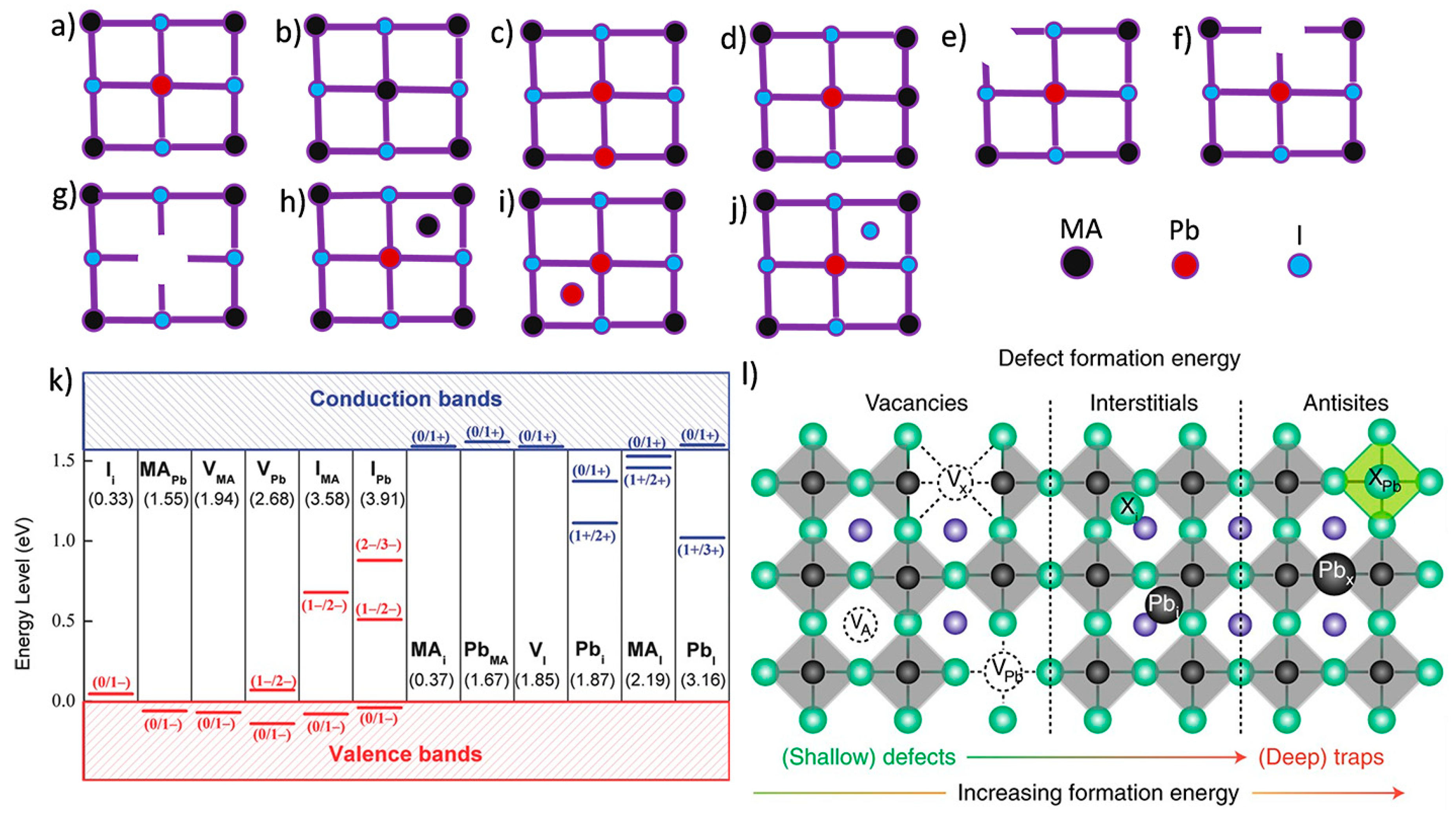
Consider the ideal crystal structure of perovskites, where each ion is located on its equilibrium site (Figure 3a). However, in reality, polycrystalline perovskite thin films are fabricated using a low-cost solution process, resulting in various structural defects and unintentional impurities during the post-treatment [78]. These structural defects can be classified as deep-level defects or shallow-level defects, depending on their thermal activation energy. Defects with a thermal activation energy higher than KBT where KB and T represent Boltzmann constant and absolute temperature, respectively, are considered deep-level defects and are suspected to be the main cause of non-radiative recombination in PSCs. The lattice imperfections other than the short-range point defects are one-dimensional (1D) dislocations, 2D-grain boundary defects, 3D precipitates, and the mobile species [79].
In perovskites, particularly methylammonium lead iodide (CH3NH3PbI3), the most widely studied defects are intrinsic ionic point defects, which have different origins [80,81]. Based on theoretical calculations, the defects in perovskite (CH3NH3PbI3) can be classified into 12 point defects: antisite substitutions (MAPb, PbI, and MAI) (Figure 3b–d, note: another three antisite substitutions IMA, IPb and PbMA are not shown in the Figure); vacancies (VMA, VI, and VPb) (Figure 3e–g) and interstitials (MAi, Pbi, and Ii) (Figure 3h–j), where MA is methylammonium (CH3NH3) [82,83,84,85,86].
It is well-known that the formation energy of a substance thermodynamically governs its stability. A substance can exist in the most stable state with the lowest formation energy. Therefore, point defects have been extensively studied theoretically by calculating their formation energies in a host perovskite crystal in equilibrium with the pure constituents (I2, Pb, and MA) based on density functional theory (DFT). Depending on their formation energies, these microscopic defects are classified as deep-level defects and shallow-level defects (Figure 3k,l). Theoretical reports suggest that point defects in standard CH3NH3PbI3 perovskite crystals that contribute to shallow or intraband states (close to CB and/or VB) have low formation energies, while those contributing to deep levels in the bandgap have high formation energies [87]. Defects such as IPb, IMA, Pbi, and PbI have high formation energies and contribute to deep-level defect states [78,88] as shown in Figure 3k. However, their high formation energies at room temperature suggest that they should not contribute to a high density of non-radiative recombination centers [80,81,89]. On the other hand, PbI and IMA defects, depending on growth conditions, have formation energies that might be high enough to make them deep-level recombination centers. Moreover, several experimental results confirm the existence of deep-level defects in perovskite films [90,91], where the predominant contributors are halide vacancies (VI) [92].
The majority of point defects in perovskite crystals, including Ii, MAPb, VMA, VPb, MAi, PbMA, VI, and MAI, have shallow-level defects due to their low formation energies (Figure 3k). These defects occupy a higher proportion of overall defect density in perovskite crystals than the deep-level defects. Huang et al. reported that the defects in the perovskites are more likely to be located within bands or the energy levels near the band edges due to the antibonding coupling in the valence band between the p orbital of iodine and a lone pair in s orbital of Pb [93].
Figure 3.
(a) Schematic illustration of an ideal MAPbI3 lattice. (b–d) Antisite defects in MAPbI3 lattice: (b) MAPb. (c) PbI. (d) MAI. (e–g) Vacancy defects in MAPbI3 lattice: (e) VMA. (f) VI. (g) VPb. (h–j) Interstitial defects in MAPbI3 lattice: (h) MAi. (i) Pbi. and (j) Ii. (k) Transition energies of point defects in MAPbI3 lattice. Reproduced with permission from ref. [80]. Copyright 2014 Wiley. (l) Distinctive defect states in MAPbI3 perovskite, including vacancies, antisites, and interstitials according to their increasing formation energy and their depths in bandgap. Reproduced with permission from ref. [89]. Copyright 2018 Springer Nature.

Although shallow-level defects are considered benign types of defects due to their much lower charge recombination rate and their little influence on the photovoltaic performance of freshly prepared devices, they possess mobile charge species that can migrate under illumination, heat, and the built-in electric field, leading to unintentional doping effects by accumulating at interfaces [94]. Light-induced ionic redistribution or the migration of defects such as interstitials, antisites, or vacancies can also cause local band bending and impede charge transportation [95], leading to anomalous hysteresis in J-V curve [96,97], degradation of perovskites or metal electrodes [98,99,100,101], and the phase segregation [102,103,104,105]. Therefore, interface defect trap states, which mainly result from the migration of ionic defects and the mismatching energy levels at the interfaces, should be mainly responsible for the non-radiative recombination losses [106].
The density of trap states in polycrystalline perovskite film is significantly higher than that in single-crystal perovskite, which hinders charge transport and shortens the charge carrier diffusion length [107,108] Polycrystalline perovskite films also contain GBs that are unavoidable during low-temperature solution fabrication, leading to structural disorder at these interfaces and the formation of defect states [109]. These defects can negatively impact the optoelectronic properties of perovskite films by reducing photoluminescence and resulting in extra loss of photogenerated charge carriers. While research has shown that trap-assisted recombination is more dominant at the interfaces than at the GBs [110], more studies focused on surfaces and interfaces using novel passivation techniques are necessary to improve the performance of PSCs.
2.4. Impact of Defect-Induced Non-Radiative Recombination on Device Parameters
The presence of trap states in perovskite thin films and at adjacent interfaces of PSCs, can severely affect their photovoltaic parameters, such as VOC, short-circuit current (JSC), and FF, thereby limiting PCE and stability. Under the bias-illumination, incident light excites electrons from the valence band into the conduction band, splitting the Fermi level (EF) into quasi-Fermi levels of electrons (EFn) and holes (EFp). The steady-state charge density, which is determined by the balance between charge generation and recombination rates, controls the quasi-Fermi level splitting (QFLS = EFn − EFp) [111]. In an ideal case with no recombination in the bulk, at the surface, grain boundaries, and interfaces, the EF of its corresponding carrier would remain constant at the quasi-Fermi level without any drop, and there would be no energy loss. In that case, the output power of the device would be equal to the QFLS [112].
However, when non-radiative recombination creates a pathway for the recombination of excess free charge carriers, it reduces the steady-state charge density and QFLS and, ultimately decreases the VOC of PSCs. Hence, non-radiative recombination is the fundamental source of the open-circuit losses [113]. The relationship between VOC, radiative and non-radiative recombination losses can be described by the external photoluminescence quantum efficiency (ηext) [66,114]:
where VOC,rad is the radiative limit of the open-circuit voltage when non-radiative recombination is fully suppressed. Therefore, the deficit in VOC due to nonreductive recombination can be expressed as [115,116]:
Thus, the voltage loss due to non-radiative recombination can be quantified by measuring the photoluminescence quantum yield (PLQY) or electroluminescence quantum efficiency (EQEEL). Improvement in PLQY and EQEEL in passivated PSCs leads to an increase in VOC and a decrease in non-radioactive recombination losses, thereby improving PCE. It has been reported that a 1% improvement in PLQY of PSCs can result in a 0.12 V increase in VOC.
Stranks et al. [102] used a potassium halides layer to passivate non-radioactive recombination centers at the surface and interface of triple-cation perovskite crystals, resulting in a high PLQY of 66% and a very low non-radiative recombination loss (Voc,non-rad = 0.11 V). Additionally, energy level mismatch between the EFn in the perovskite layer and the CB of ETL or between the EFp in the perovskite layer and the VB of HTL can cause band bending at the interfaces, leading to a reduction in the QFLS and a loss in VOC. In addition to affecting VOC, non-radiative recombination also has a pronounced effect on the FF of devices. The maximum FFmax of PSCs can be calculated as the following Equation (4) [117]:
As shown in Equation (4), the FFmax of PSCs is closely related to VOC. Since VOC is highly influenced by non-radiative recombination, as discussed in Equation (3), FFmax is also expected to be affected by non-radiative recombination. The recombination at the surface and GBs also influence the charge extraction efficiency, potentially affecting the JSC and FF of PSCs [110]. Defects passivation may reduce the contact resistance at the absorber/charge transport layer interface, and the addition of passivation agents into perovskite precursors may even change the film morphology, resulting in fewer pinholes as shunt paths, which can improve FF in PSCs. Optical losses, which stem from photon reflection or poor absorption in poorly responding cell regions, are mainly responsible for the lower value of JSC. Furthermore, electrical losses originating from finite resistance in the light absorption layer, defects within the transport layer, and poor contact between the transport layer and the electrodes affect charge extraction, increasing the series resistance, which reduces FF [110,118]. Furthermore, micro-cracks, scratches, and other severe defects on the perovskite surface can cause increased surface roughness, which in turn affects FF.
2.5. Defect Induced Hysteresis Behavior and Intrinsic Instability
The hysteretic behavior in the J-V characteristic of PSCs presents a challenge to accurately characterize their photovoltaic performance. Although the exact reasons for this behavior are still under debate, many studies suggest that charge defects and ions migration (Figure 4a–d) [119,120] are responsible for the anomalous hysteresis observed in the J-V characteristics of different scanning directions [121,122]. Despite achieving impressive PCE values, most PSCs still suffer from hysteresis [123] and instability [124], which are associated with varying amounts of active charge defect states in the perovskite thin films and device interfaces [119,120]. Ion migration induces intrinsic defects and affects the electric field distribution at interfaces. By using the time-resolved Kelvin probe force microscopy (tr-KPFM) technique, Stefan et al. demonstrated that the hysteresis in PSCs is caused by the localized positive ionic space charge at the ETL surface and negative ionic space charge across the perovskite layer. These charges form an opposite charge layer at the perovskite/ETL interface upon illuminating or applying external voltage (Figure 4e–h). Thus, they attributed the hysteresis to the formation and release of ionic interface charge caused by the variation in illumination or electric field [122]. Their results also confirm that the ion migration toward the interface region impedes the smooth charge extraction and transportation. However, the interplay between ion migration and interfacial defects still requires further exploration.
Several approaches have been proposed to suppress hysteresis in PSCs. One of the most effective methods is the use of additives for the interface, GBs, and ionic defects passivation. FA-based and mixed cationic perovskites have also been found to demonstrate less hysteresis than MA-based PSCs. Another promising technique is the fabrication of 2D/3D graded junctions, which has been shown to reduce hysteresis in mixed-dimensional PSCs. Additionally, an appropriately high scanning rate and improving the crystallinity of the perovskite layer have been found to suppress hysteresis in the PSCs. However, it should be noted that sometimes, scanning direction and rate do not influence the hysteresis. Moreover, the inverted structure device has been found to show less hysteresis compared to regular structure devices. The presence of hysteresis is one of the limitations of developing PSCs. To fully optimize the devices, it is essential to have an accurate understanding of the hysteresis and its effect on PSCs.
Figure 4.
(a) Ion migrations in MAPbI3 perovskite absorber for VI defects. (b) Ion migrations for VMA defects. (c) Ion migrations for VPb defects. (d) Ion migration for Ii defects. Reproduced with permission from ref. [24]. Copyright 2015 Royal Society of Chemistry. (e–h) Demonstration of how the ion migration causes hysteresis in MAPbI3 solar cell: (e) Field-free absorber layer (f) under the applied electric field across the device the immediately the mobile I− ions accumulate the anode interface while electric field drives electrons towards the cathode and holes towards the anode. The drifted ions start to screen the external voltage. Additionally, ions are adsorbed at the cathode interface. (g) The complexation and neutralization (X+-I−) at the cathode is reducing the perovskite from mobile ions. Positive charges at the anode interface are compensated by electrons from the fluorine-doped tin oxide (FTO). These charges now screen almost the entire electric field, and the potential is flat across the perovskite layer. (h) Upon switching off the field between the electrodes, the slow release of the separated charges at the interfaces keeps a reverse electric field in the perovskite layer. This reverse field aids in driving electrons towards the anode and holes towards the cathode. Reproduced with permission from ref. [122]. Copyright 2018 Royal Society of Chemistry.

Charge defects and ion migration triggered by light or heat not only cause hysteresis but also severely induce intrinsic instability in the PSCs [24]. During the low-temperature fabrication of the perovskite active layer, a high density of defects (1016–1018 cm−3) is unavoidably generated [125]. Moreover, due to the moderately weak chemical bonds in the perovskite lattice, the low-energy defect formation process remains active with even slight external influence. These defects, which are ionic in nature, do not significantly affect the performance of a freshly prepared device. However, the migration and accumulation of these ionic defects towards the interfaces can rapidly degrade the perovskite material and charge transport layers (CTL). The damaged interfacial layers can allow moisture to react with the perovskite, which further accelerates the degradation of devices under ambient conditions, seriously hindering the commercial application of PSCs. To mitigate the adverse effect of ionic charge defects, successful techniques include 2D/3D mixed perovskites, which reduce the number of defects and significantly improve device stability. Additionally, it is known that the movement of iodide ions is a significant source of instability and hysteresis [126]. Therefore, passivating with additives and interface engineering are the other most successful techniques for obtaining high efficiency and improved stability of PSCs.
3. Estimation of Defect-Induced Recombination Losses and Techniques for Calculating Defect Density
As mentioned earlier, trap-assisted recombination mostly affects VOC and FF. Therefore, calculating the VOC deficit provides an overall measure of the loss resulting from non-radiative recombination occurring at the interfaces and grain boundaries and in the bulk. Accurately quantifying the VOC deficit is useful for analyzing the passivation effect of additives and for designing new passivation molecules to further enhance device performance. We can calculate the VOC deficit by accurately calculating the bandgap and measuring the photoluminescence quantum efficiency (PLQE) or the external radiative efficiency (ERE).
3.1. Calculating the Bandgap
Accurately estimating the bandgap of semiconductor materials is crucial for precise calculations of the VOC deficit caused by trap-assisted recombination occurring in bulk or device interfaces. However, the presence of a substantial number of defects and variation in perovskite film thickness can make it challenging to estimate the bandgap accurately, leading to underestimation or overestimation of recombination losses in the form of VOC deficit in PSCs. Various techniques, such as Kubelka–Munk processes, Tauc plots, and the onset of electroluminescence quantum efficiency (EQE) spectra are used to calculate the bandgap of perovskite thin-film material [127]. The Kubelka–Munk technique calculates the bandgap by measuring the reflection of incident light, while the Tauc plots method utilizes the absorption of incident light in a wide spectral range to determine the bandgap. However, the accuracy in the calculated bandgap for thicker perovskite film is less reliable due to sub-band absorption, resulting in an underestimation of its value. The observed redshift of the onset of EQE spectra is also due to the absorption by electrically active sub-bands. Nevertheless, the effect of absorption by the active sub-band on determining the bandgap can be reduced by using the differential of EQE spectra [128]:
In the above equations, a and b represent the integration limits, E represents the photon energy, and the probability distribution function for the bandgap energy is defined by P(Eg). Furthermore, taking the photon energies for the P(Eg) calculation equal to 50% of the EQE peak value can help reduce additional noise.
3.2. Photoluminescence Quantum Efficiency
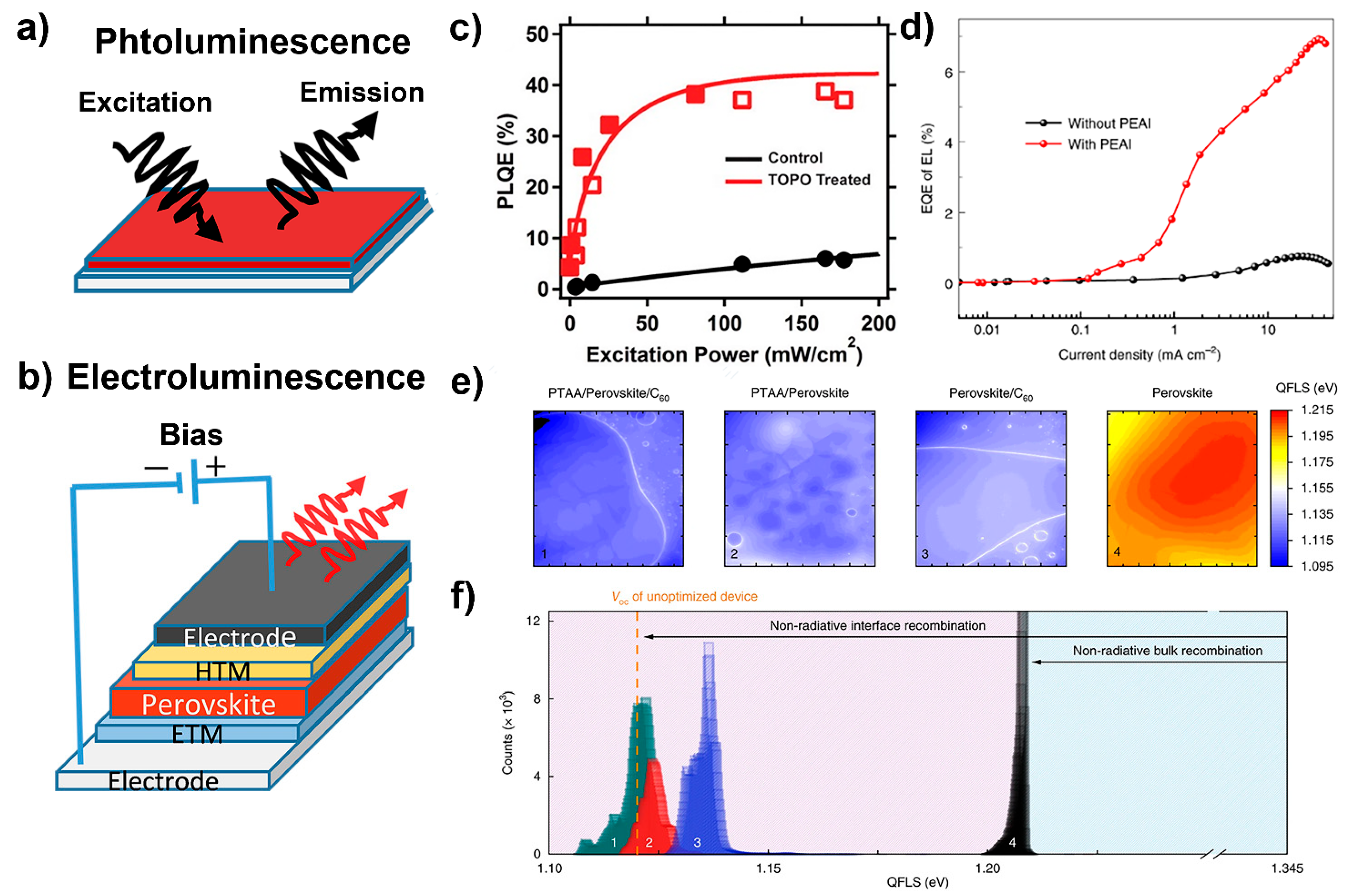
High photoluminescence quantum efficiency values approaching unity indicate suppression in non-radiative recombination, which is desirable to achieve PCEs close to the theoretically calculated values for single-junction PSCs. If the PLQE value reaches unity, it can be inferred that all non-radiative recombination pathways have been eliminated, and charges are recombining through the emission of photons. When measuring PLQE, incident photons with excitation intensity equivalent to 1 Sun excite carriers to all accessible states, ignoring any imbalance in carrier transport. The relationship between output VOC and the photoluminescence quantum yield (PLQY) is given as [66,129]: . At 1 Sun and excitation density of 1015 cm−3, an increase in PLQY from 1% to unity results in 0.12 V increase in VOC. The obtained PLQY spectra depend on film quality, energy levels matching ETL or HTL with the perovskite layer, and the interfacial recombination channels, as well as other optical losses such as photon escape and parasitic absorption. As PSC is composed of a complex, layered structure, recombination losses in the intrinsic perovskite layer and at the interfaces can be quantified separately. For example, the PLQY of the perovskite layer can be calculated separately by depositing it on a quartz substrate, as shown in Figure 5a, and then the interfacial recombination loss can be estimated by measuring PLQY when the perovskite layer is in contact with the ETL or the HTL (Figure 5b). In this case, a decrease in PLQY value reflects the presence of recombination pathways at the interfaces. The defects introduced at the interfaces may create a barrier for electrons and contribute to their recombination at interfaces, leading to significant loss to the PCE [130]. Moreover, defect passivation can suppress non-radiative recombination and enhance PLQE. For example, Ginger et al. [131] treated perovskite films with tri-n-octylphosphine oxide (TOPO), resulting in devices exhibiting a 35% PLQE compared to 3% for control film, as shown in Figure 5c.
3.3. External Radiative Efficiency
Estimation of VOC deficit induced by trap-assisted recombination is often performed using the external radiative efficiency (ERE) under a forward bias with an external voltage source. ERE is typically measured when the injected current under bias is equal to the illumination current. The value of ERE indicates the extent of losses due to non-radiative recombination. A high ERE value indicates low non-radiative recombination losses, suggesting that sufficiently large injected current emits the photons by radiative recombination of carriers [132]. However, the ERE of a complete PSC is generally lower than the PLQY of a perovskite active layer measured alone or in a complete device due to the inequalities in the spatial distribution of the quasi-Fermi levels. The value of ERE can only be compared with the PLQY if the distribution of QFLS remains flat in both measurements. For planar PSCs, the high reabsorption and low light-out coupling efficiency (20–25%) contribute to lower ERE compared to PLQY [66,134]. The VOC can be estimated by using the equation [135,136]:
When the ERE value is one, the radiative recombination reaches its theoretical limit, and each time ERE is reduced by an order of magnitude, there is an approximately 60 mV deficit in VOC. The best electroluminescence (EL) efficiency exhibits up to 8% [132] for the phenethylammonium iodide (PEAI)-modified device, as shown in Figure 5d, which is higher than that of single-junction silicon (Si) solar cells (ERE = 2%) [137]. However, gallium arsenide (GaAs) solar cells, which yield higher PCE than the Si solar cells, exhibit ERE of 32.3% [65], indicating that there is significant potential for improvement in ERE from PSCs. Nevertheless, when measuring the electroluminescence of a complete perovskite device, two drawbacks must be considered. Firstly, in a forward-biased PSC, the unbalanced transport of electrons and holes (because of the preference of injected charge carriers to occupy the lowest-energy states) hampers carrier transport in the perovskite active layer [138]. Secondly, the forward biasing electric field can encourage ion migration in the perovskite layer, and the ion dislocation produces internal electric fields [139,140]. Consequently, the external electric field accountable for the movement of the carrier towards the emissive regions is screened by an internal electric field. This phenomenon increases the uncertainty in the measurement of non-radiative recombination losses. Therefore, comparing the ERE with the measured PLQY of a complete device may be a realistic strategy for the accurate estimation of non-radiative recombination losses [129].
3.4. Photoluminescence Imaging
The defect states responsible for non-radiative recombination in perovskite absorbers are distributed randomly throughout the bulk, surface, and interfaces. However, the regions near the surface of perovskite film are believed to have a high concentration of trap states. Hyperspectral absolute photoluminescence imaging is a commonly used technique to identify the origin and spatial distribution of defect states in complete PSCs and effectively quantify the trap-assisted recombination losses caused by the defect states at bulk, bottom, and top interfaces (Figure 5f).
By using this technique, Stolterfoht et al. [133] showed that the non-radiative recombination losses in the active area are sufficiently non-uniform, and their corresponding losses result in decreasing the QFLS. The interfacial recombination after the incorporation of each charge transport layer individually with perovskite layer (such as poly[bis(4-phenyl)(2,4,6-trimethylphenyl)amine] (PTAA) as HTL and fullerence (C60) as ETL) results in an 80 meV drop in the QFLS at each interface (Figure 5e). It is important to note that the loss in VOC due to non-radiative recombination induced by each layer does not simply add up in complete perovskite device operation. Rather, the overall VOC deficit is attributed to the increase in the trap-assisted recombination current, which has a logarithmic relation with VOC. Therefore, each individual recombination channel within a complete perovskite device plays an important role, and their comprehensive understanding is necessary for improving the performance of PSCs in the future.
3.5. Thermal Admittance Spectroscopy (TAS)
Understanding defects and the depths of their energy levels is essential for reducing non-radiative recombination losses in PSCs. TAS is used to obtain detailed information on the trap density of states (tDOS) in a complete PSC. Charged defects in the photoactive layer act as small, localized capacitors, and the trapping-detrapping of carriers in defects is related to the charge-discharge process in the capacitor. By tracing variations in junction capacitance with the frequency of applied alternating current (A.C.) voltage, the features of defects can be deduced. In its working process, first the charged defect states are thermally activated, then they release their charge within the A.C. period and capably foster the admittance signal. The discharging of defects depends on both the depth of the defect energy level and the temperature, which can be reflected by the junction capacitance at varying modulated A.C. frequency. The energy Eω of the defect energy state at a frequency (ω) could be assessed as [78,90]:
In the above equation, Ed and Ev represent the depth of defects energy level and the valance band maximum, respectively. The defect density (Nt) derived from angular frequency-dependent capacitance is given by Equation (8):
In Equation (8), ω stands for angular frequency, and C denotes the capacitance. Vbi is a built-in potential and is derived from the capacitance-voltage (C-V) curve. W represents the depletion width, which is taken from Mott-Schottky analysis and expressed as [78,141]:
In Equation (9), A and εr represent the contact area and relative dielectric constant. Measurements using TAS reveal a larger density of defect states (∼1018 cm−3) in a complete PSC compared to the density of defects in a sole perovskite film in isolated form. The defects induced tDOS having different energy depths usually be categorized into three bands: band 1 lies in an energy interval of 0.35–0.40 eV, band 2 lies between 0.40–0.50 eV, and band 3 lies above 0.50 eV (Figure 6a). Some useful approaches for reducing the tDOS include coating a layer of phenyl-C61-butyric acid methyl ester (PC61BM) on the surface of the perovskite active layer, which can effectively decrease the tDOS of band 2 and band 3 almost two orders of magnitude (Figure 6a), and surface passivation, which can substantially reduce the deep-level defect states. Nevertheless, identifying the nature and origin of all kinds of defects using only TAS is challenging. A surface-sensitive technique, such as scanning tunneling microscopy (STM), can accurately provide defect information in a single perovskite crystal, but the high roughness of polycrystalline film limits its use.
3.6. Steady-State PL Emission
In addition to electrical properties, defects can strongly affect the optical properties of perovskite semiconductors. Therefore, steady-state PL emission has been widely used to estimate the defect density in perovskite films for photovoltaic applications [78,144]. Initially, the perovskite film is photoexcited with pump fluence. After photoexcitation, either the excited charges in perovskite film emits photon through the band-to-band transition, or they become trapped in defect states, resulting in negligible or no emission. If all the defect traps are filled with the photogenerated charges in perovskite thin film, this is indicated by a turning point at low pump fluence, also known as a trap filling turning point. The trap filling turning point at low pump fluence is called a threshold trap pump fluence () which can be determined by the intersection of the pump fluence axis and linearly extrapolated PL intensity. The total defect density ntrap can be assessed by the following equation [78,144,145]:
The term α in Equation (10) stands for the absorption coefficient, whereas E represents the energy of a single photon at the laser pulse wavelength. A higher accuracy in calculating the total defect density can be achieved by using an increased pump fluence for PL emission. Furthermore, this technique enables the estimation of defect densities in the surface and bulk of the perovskite material. However, the depth of the defects’ energy level cannot be inferred from its experimental data, which is the drawback of this technique.
3.7. Space Charge Limited Current (SCLC)
The SCLC technique is another widely used characterization tool for quantifying defect density and carrier mobility and understanding defect-induced trap mechanisms inside the PSCs [142,146,147,148]. In this technique, an adequately large electric field is applied to an electron- or hole-only device via Ohmic contacts and a portion of the ejected electrons/holes is trapped by the defects in perovskite, reducing the density of free charges and limiting the current by the space-charge effect. The dark J-V curves obtained from this technique exhibit three regions: the Ohmic or the linear region, trap-filling limit (TFL) region, and the SCLC region, which is trap-free. The linear region represents the Ohmic response, where current density and electric field intensity have a linear relation (I ∝ V). The trap-filling region shows a rapid increase in the current with increasing the electric field (I ∝ Vn, n > 3), where defect states are continuously filled until all the defects are filled as bias increases. Subsequently, the SCLC trap-free region (I ∝ V2) occurs. The trap density (nt) can be calculated using the following equation:
where, ε represents the dielectric constants for the photoactive layer, ε0 represents the vacuum permittivity, L represents the thickness of the perovskite active layer, and q represents the elementary charge. VTFL is the bias voltage required to occur the TFL region, which can be obtained from the dark J-V by fitting (Figure 6b). The dielectric constant of the photoactive layer (perovskite) can be calculated from Equation (12):
where, Cg denotes the geometrical capacitance of the active layer, ε0 = 8.85 × 10⁻¹⁴ F·cm−1 is permittivity of free space, and A represents the active area of the device [149]. Note that this technique only calculates the single type of defects for electron traps or hole traps at a time.
3.8. Deep-Level Transient Spectroscopy (DLTS)
DLTS is a technique that is used to detect deep-level traps that are difficult to detect by other characterization techniques [78,143,150,151]. It is significant because of its sensitivity, ease of operation, and its ability to set a window for emission rates [150]. The DLTS utilizes the variation in defect emission rates with temperature to define the energy difference between one of the band edges and the defect states in the forbidden gap and to estimate the capture cross-section of the defects [143]. The capacitance transients are explored using the DLTS technique by evaluating the variations in capacitance with variation in temperature (from the temperature of liquid nitrogen to the room temperature or above). The defect states are filled up by the charges generated under an initial low-temperature bias pulse. In this case, the emitting rate of a trap state is much lower than its capturing rate and the former can be neglected [78]. Upon increasing the temperature, if the emission rate is found in the rate window, the DLTS peaks will gradually appear as shown in Figure 6c (three peaks appear in control film denoted by A1, A2, and A3). The defect density can be estimated directly from the capacitance change, corresponding to complete filling of the trap states with a saturating injection pulse. The defect density at a particular temperature can be calculated by Equation (13) [150]:
where, ΔC represents the capacitance change due to a saturating injection pulse, C represents the capacitance of diode, and (NA − ND) denotes the net acceptor concentration on the p side of the junction. Additionally, the ΔE of the defects below CB can be calculated by Equation (14) [150]:
In the above equation, the terms <νn>, en, and σn stands for the mean thermal velocity of charge carriers, the rate of thermal emission of the trapped carriers, and the charge capture cross-section, respectively. And and ND represents the degeneracy of the defect and the effective density of states in the carrier band. ΔE stands for the energy separation between the trap level and the minority-carrier band. DLTS is a useful technique providing information related to concentration profile, electron- and hole-capture cross-section of the different defects and the ΔE of defects. However, the minority charge trap states might be missed in DLTS data as the forward current cannot fill them. Thus, a defect level during the fall time of the pulse might be empty even if it is saturated during the injection pulse [140,150]. Furthermore, the transient disappears, and defects (such as acceptors, bound exciton, and donors form shallow centers) cannot be filled between pulses if the optical emission rate is much lower than the thermal emission rate. Hence, a high thermal emission rate makes the DLTS unable to observe shallow-level defects.
4. Novel Defect Management Strategies to Mitigate Defect-Induced Losses and Instability Issues
The presence of disorderly lying defect states in perovskite solar cells is a well-known issue that hinders both device efficiency and stability. Multilayered perovskite solar cells are particularly susceptible to surface and interface defects during the fabrication process, with ionic defects generated during thermal annealing and interfacial defects from nonradioactive recombination centers leading to reduce the charge extraction and transport. In this section, we will review recent progress in improving the performance and stability of the PSCs through novel defect suppressing techniques, including compositional engineering, additive engineering for surface and GB passivation, dimensionality engineering, and the interfacial layers engineering.
4.1. Bulk or the Deep Level Defects Passivation Techniques
4.1.1. Compositional Engineering
Compositional engineering is one of the most successful techniques for regulating the optoelectronic properties of perovskite thin films, including light absorption, carrier mobility, defect density, and carrier concentration. This method allows for the modification of the perovskite film morphology and crystallinity through cationic or ionic doping [152,153]. For instance, the regular perovskite composition, MAPbI3, has corner-connected PbI6 octahedra, with MA+ cations occupying the interstices. At room temperature, the pure MAPbI3 phase is tetragonal. Generally, perovskites have the formula ABX3 (Figure 7a), where A represents a mono-cation such as methylammonium (MA), which can be substituted with formamidinium (FA), or cesium (Cs), or the mixed cations. B represents a metallic divalent cation Pb2+, which can be substituted with Sn2+, and X represents iodide, which can be substituted with other single or mixed halides. The flexibility to substitute A, B, or X ions in the pure perovskite structure makes hybrid perovskites highly suitable for photovoltaic applications. This flexibility enables the customization of the optical and electrical properties (Figure 7d–e) to meet specific requirements [154,155] Whether a particular composition can form a perovskite crystal structure can be predicted by estimating Goldschmidt’s tolerance factor t (Figure 7f), which is given by the equation, , where rA, rB and rx are the radii of ions in the perovskite ABX3 [156,157,158]. A perovskite can be stabilized when the tolerance factor falls within the range of 0.8–1 [159]. It has been reported that the A-site organic cation in lead halide perovskite lattice indirectly influences its structural stability and electrical properties. The Pb-I-Pb bond angle and Pb-I bond length are likely affected by the A-site cation, and the variation in these bond angles and lengths can influence the valance band maximum (VBM) and conduction band minimum (CBM) of perovskite semiconductor [160,161]. Similarly, the alteration of the B-site cation or halide anion can directly influence the VBM and CBM as the B-X bond determines band structure [161,162]. For instance, Park et al. claimed that excess lead iodide in the bulk perovskite can suppress the halide vacancy and govern the crystal orientation in the vertical direction towards the substrate [163].
Hence, the optoelectronic properties of perovskite are directly or indirectly influenced by A- and B-site cations and X-site anions [153]. Engineering at the cationic or anionic sites through mixed anions and cations or suitable substitution in standard perovskite structure can suppress non-radiative recombination and improve PCE and stability. This section reviews the progress made in PCE and stability in PSCs using different compositions.
X-site engineering: Early PSCs made with MAPbI3 exhibited low PCE due to poor crystallinity and morphology of the perovskite film. However, Jeon et al. were able to achieve a PCE of 16.2% by substituting Br for I in the perovskite composition and using the anti-solvent dipping technique to suppress defects during crystal growth [164]. Noh et al. also achieved a PCE of 12.3% by using a mixed halide MAPb(I1−xBrx)3 composition to tune the bandgap and improve the device stability [165]. The mixed composition MAPb(I1−xBrx)3 can tune the bandgap in the range from 1.53 eV to 2.97 eV (see Figure 7e) and provides high-efficiency colored PSCs [165,166]. Additionally, the addition of Cl− to MAPbI3 as an additive in the precursor has been shown to improve PCE by increasing carrier diffusion length [167]. Mixed halide composition has proven effective in improving perovskite film growth and tuning optoelectronic properties of the material, but the phase segregation or halide segregation in mixed halide perovskite can still negatively impact their stability.
Similarly, anion engineering with halides [168] or the pseudo halides such as thiocyanate (SCN−) [169], formate (HCOO−) [170] could also stabilize the α-phase FAPbI3 with optimized tolerance factor and reduced lattice constant. For example, in 2022, Jeong and coworkers [170] reported that after introducing some trace of formamidine formate (FAHCOO) (x mol %, x ≤ 4) into the perovskite precursor, the pseudo-halide anion formate (HCOO−) can suppress anion-vacancy defects at the surface and GBs and enlarge the crystal size of the formate-doped FAPbI3 (Fo-FAPbI3) film, which also achieve a high PCE of 25.6% (certified 25.2%) as well as a long-term operational stability of 450 h.
Both A and X sites engineering: The large bandgap of MAPbI3 (∼1.55 eV), which is greater than the Shockley–Queisser optimum of ∼1.4 eV for single-junction solar cells, means that it cannot absorb the full solar spectrum. Doping with the larger formamidinium (FA) cation can reduce the bandgap to around 1.48 eV (Figure 7d), improving optical and electrical properties and leading to higher JSC and PCE of PSCs. Additionally, reports suggest that the MA cation rotation can passivate deep-level defects such as iodide and lead vacancies, making A-site cation more influential in the traps, charge transport, and light absorption of perovskite devices. FA is more thermally stable than MA cation, making it a suitable doping candidate for device stability (Figure 7b–c). Pellet et al. reported the first A-site doping with FA cation to fabricate mixed cation (MAxFA1−xPbI3) PSCs in 2014. A-site engineering significantly improved light absorption, JSC, and the PCE of the devices [171]. Further improvement in crystal morphology and phase stability was realized when mixed cations and mixed halides were used [172]. Yang et al. reported the fabrication of high-efficiency PSCs from mixed cations (MA, FA) and mixed halides (iodine (I), bromine (Br)) solutions by a two-step spin-coating method, which suppressed deep-level defects and maintained the α-phase of FAPbI3 perovskites [151]. The additional I− passivated deep-level defects, and Br− improved the crystallinity of perovskite films. The resulting perovskite had a bandgap of 1.51 eV, with a certified efficiency of 22.1% in small area devices and 19.7% in 1 cm2.
Figure 7.
(a) The standard perovskite crystal structure ABX3. Reproduced with permission from ref. [166]. Copyright 2014 Royal Society of Chemistry. (b,c) Replaceable cations at A-site in perovskite lattice. Due to its volatile nature, MA cation thermally degrades at a temperature of 80 °C compared to rubidium (Rb) or Cs, which are thermally more stable. Reproduced with permission from ref. [173]. Copyright 2018 American Association for the Advancement of Science. (d) Ultraviolet-visible (UV-Vis) absorption spectra for the APbI3 perovskites formed by tuning the bandgap with the replacement of the A-cations, where A is either FA, MA, or Cs. Reproduced with permission from ref. [166]. Copyright 2014 Royal Society of Chemistry. (e) Tauc plot for bandgap determination of MAPbX3, where X is either I, Cl, or Br. (where the asterisk symbol (*) denotes the multiplication sign) Reproduced with permission from ref. [153]. Copyright 2015 Wiley. (f) Energy difference between α-phase and different δ-phases for FA1–xCsxPbI3 alloys with different Cs ratios. Reproduced with permission from ref. [159] Copyright 2015 American Chemical Society. (g) Illustration of maximum achievable PCE and JSC theoretically as a function of the bandgap (Eg). Replacement of MA to FA cation causes a moderately small change of 0.1 eV. While the halide change (I-Br) causes a large change of 0.7 eV. Reproduced with permission from ref. [173]. Copyright 2018 American Association for the Advancement of Science.

The addition of Cs to mixed organic cations (FA, MA) solution for the formation of triple cation mixed halide perovskite has been shown to improve the stability and photovoltaic performance of devices. PSCs fabricated from these perovskite solutions have a bandgap of up to 1.63 eV (Figure 7g) and produce higher VOC of 1.24 V [135]. In 2016, Saliba et al. reported the use of triple cations perovskite solution for PSCs, resulting in enhanced efficiency, stability, and reproducibility. They found that the addition of a small amount of Cs in FA/MA-based solution prevented the photo-inactive yellow phase by reducing the effective radius of FA/MA composite and bringing it close to the tolerance factor of the cubic lattice. The resulting triple cation solution was able to crystalize into defect-free high-quality films. With optimized cationic concentration, they achieved a PCE of 21.1%, which remained at ∼18% after a standard test for 250 h [20].
In 2019, Matsui et al. [174] conducted experiments to explore the relationship between thermal stability and the perovskite composition. They chose Cs0.05(MA0.17FA0.83)0.95Pb(I0.83Br0.17)3 perovskite composition, which has previously been reported to be highly efficient and thermally stable. They found that excess rubidium (Rb) in precursor suppressed the growth of lead iodide (PbI2), even in PbI2-rich precursors. However, reducing the Br ratio in perovskite crystal was necessary to prevent rubidium bromide (RbBr)-based aggregations that decrease device performance. They determined that the optimized perovskite composition for stability and PCE was Rb0.05Cs0.05FA0.75MA0.15Pb(I0.95Br0.05)3, which retained 92% of its initial PCE of 20.6% after 1000 h of testing at the international standard of 85 °C/85% relative humidity (RH).
Many reports confirm the little excess PbI2 in the precursor is better for GBs defects passivation and elimination of hysteresis in planar PSCs. Jiang et al. [175] investigated the effect of PbI2 content on hysteresis, PCE, and stability of mixed composition planar PSCs. They found that a moderate amount of residual PbI2 at GBs was beneficial for passivating GB defects and eliminating hysteresis in the devices, while too much residual PbI2 led to lower stability and severe hysteresis. With an optimized PbI2 concentration, they achieved a certified PCE of 20.9% in a device with an active area of 0.073 cm2, demonstrating higher stability and efficiency without hysteresis.
Recently, Bu and coworkers [176] reported an efficient fabrication method for high-quality FA/Cs perovskite films by incorporating methylammonium chloride (MACl), PbI2, and potassium hexafluorophosphate (KPF6) in the FA0.88Cs0.12PbI3–perovskite precursor solution. This approach significantly reduced the formation energy, enhanced the crystallinity, and passivated both the GBs and the surface of the perovskite films. Consequently, the resulting small-sized solar cells exhibited a high PCE of 24.02%, while the solar mini-module with a size of 5 cm × 5 cm demonstrated a PCE of 20.5%.
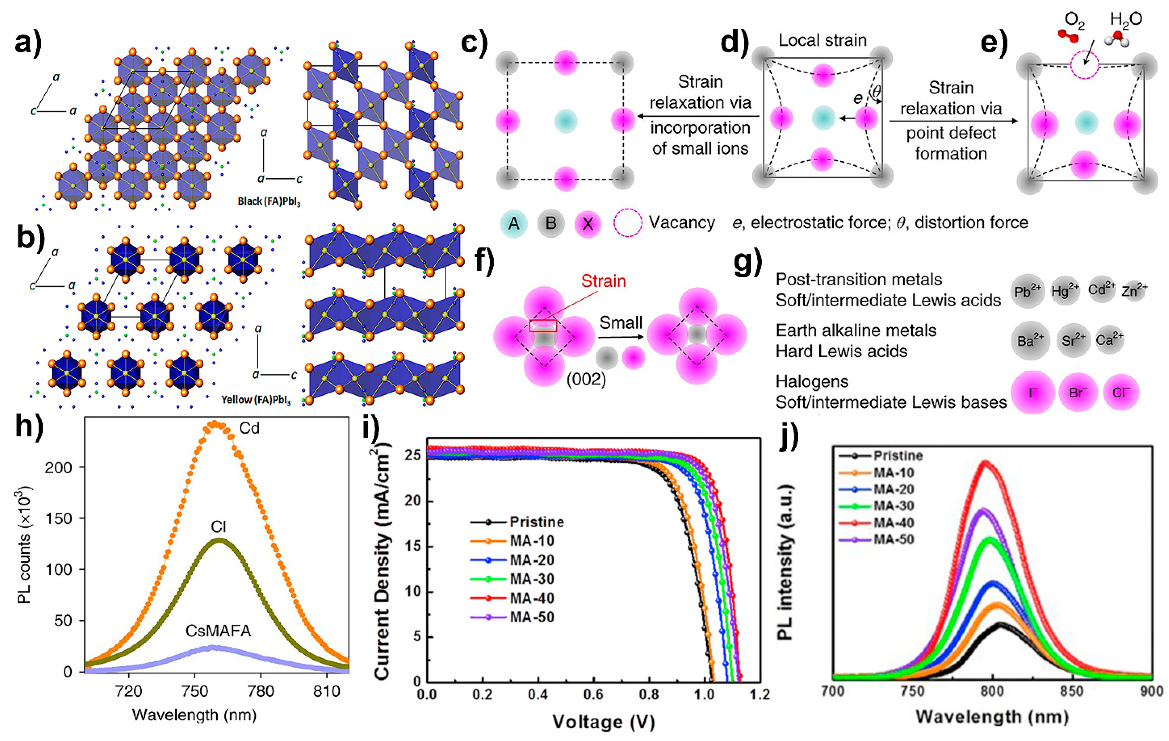
Stabilizing the photoactive α-phase of FAPbI3: Compared to MAPbI3-based PSCs, FAPbI3-based PSCs have a reduced bandgap of 1.48 eV due to the slightly larger size of FA cation (Figure 7b–d), which enhances light absorption and potentially leads to higher JSC and PCE closer to the SQ limit. However, their stability is comparatively lower than that of MAPbI3-based perovskite due to their tolerance factor, which falls close to the upper boundary of the Goldschmidt chart. Moreover, the structural instability of FAPbI3 at room temperature remains a challenge as it can crystallize to an undesired, photo-inactive hexagonal δ-phase with a wide bandgap [177] (Figure 8a,b). The room-temperature stable hexagonal phase has a high tolerance factor and activation energy, which can be reduced by using mixed cations, anions, or additives to promote the formation of the desired stable black perovskite phase (see Figure 7f). However, even the trigonal photoactive α-phase or a black perovskite phase is also sensitive to humidity and high α-phase transition temperature, which makes this composition more challenging.
One approach to achieve the pure perovskite phase in FAPbI3 perovskite is by using mixed cations and anions compositions. For example, Jeon et al. [33] reported stabilizing the α-phase of FAPbI3 perovskite by modifying its precursor with methylammonium lead tribromide (MAPbBr3), resulting in a high PCE exceeding 18% for an optimized composition of (FAPbI3)0.85(MAPbBr3)0.15. However, additional halide content can increase bandgap and cause halide segregation, leading to PSC instability. Another approach is to form a thin layer of low dimensional perovskites on 3D perovskite, which has been shown to stabilize the α-phase of FAPbI3-based PSCs. Guaninium (G) organic spacer-based low-dimensional perovskites have also been investigated, achieving a high PCE of up to 16% in the G2FA1−nPbnI3n+1 perovskites [178].
Recently, researchers have produced highly efficient FA-based PSCs by using additive to stabilize its fast photoactive black phase and suppress the defect density. The use of alkali metal cations along with mixed cations composition in the precursor solution can help to improve morphology and stabilize the pure perovskite α-phase. For example, in 2018, Turren-Cruz et al. [173] achieved the highest stabilized PCE of 20.35% in optimized Rb5Cs10FAPbI3 perovskite composition. Similarly, in 2019, Min et al. [179] reported the highest stabilized PCE of 23.7% by stabilizing α-phase of MA+, Cs+, and Br− free pure FAPbI3 with 3.8 (mol %) methylenediammonium dichloride (MDACl2) additive, where MDA2+ cation doped into the lattice to stabilize the crystal structure and Cl− helped to improve the morphology and the crystallization. In the same year, Kim et al. [180] used 40 mol % MACl to stabilize an intermediate α-phase FAPbI3 perovskite by cationic site substitution, achieving a high certified PCE of 24.2%.
The lattice strain in FAPbI3 perovskite can produce vacancy defects due to the mismatch between the size of the lead halide cage and the A-cation (Figure 8c–e), resulting in the tilting of the PbX6 octahedra and distortion of the cage (Figure 8f). The introduction of isovalent, smaller ions can alleviate this lattice strain [181] (Figure 8g). In 2020, Kim et al. [42] achieved a stabilized efficiency of 24.4% in FAPbI3-based PSCs by substituting FA sites with a very small amount (0.03 mol %) of methylenediammonium (MDA) and cesium (Cs) cations. The synergistic effect of MDA and Cs cations lowered the lattice strain, stabilized the perovskite black phase, and increased carrier lifetime by passivating defects.
Compositional engineering is an efficient approach to improving the performance and stability of PSCs. Optoelectronic properties of perovskite are directly or indirectly affected by both A- and B-site cations and X-site anions. Engineering at cationic or anionic sites either by mixed anions and cations or suitable substitution in a standard perovskite structure can lead to suppression of non-radiative recombination and improvement in PCE and stability.
4.1.2. Bulk Passivation with Alkali Metal Cations
Defects such as iodine interstitials (Ii) in the perovskite absorber are generated during the growth process, resulting in an accelerated non-radiative recombination of photo-generated electron-hole pairs and decreased PCE of the perovskite devices. These iodine interstitials can readily migrate due to their low activation energy (0.29 eV) [182], causing undesirable current-voltage hysteresis and device instability [182,183]. Both the theoretical and experimental results confirm that the introduction of alkali metal halides (potassium iodide (KI), cesium iodide (CsI), lithium iodide (LiI), cesium chloride (CsCl), sodium fluoride (NaF, etc.) into the perovskites solution effectively suppresses bulk defects as well as defects along surface and GBs, inhibiting ions migration and anomalous hysteresis, and thereby improving carrier lifetime and the overall device performance. Qiao et al. [184] reported that the addition of alkali metal cations increases the defect formation energy and reduces defect concentration. If defects are formed, alkalis strongly bind to them and reduce their charge-trapping ability, thereby increasing carrier lifetime in MAPbI3. Their simulation result shows that the carrier lifetime of the passivated perovskite layer is extended seven times that of the control MAPbI3.
Abdi-Jalebi et al. demonstrated that the addition of an optimized amount of potassium iodide (KI) solution in triple cations perovskite (Cs0.06FA0.79MA0.15)Pb(I0.85Br0.15)3 solution successfully suppresses the non-radiative recombination by passivating halide vacancies and eliminates hysteresis by suppressing photoinduced ion migration in perovskite films [102]. The improvement in luminescence yields was attributed to the decrease in bandgap and surface and GBs defects passivation by the formed layer of KI at the surface of perovskite absorber layer. The origin of hysteresis in PSCs, as confirmed by several theoretical studies, is not the migration of iodine vacancies but the formation of Iodine Frenkel (I Frenkel) defects [41]. Based on density functional theory (DFT) calculations, it was reported that K+ ions with radii of 1.38 Å preferably occupy the interstitial sites in the perovskite lattice than the other alkali metal ions and serve as the most effective passivation agent for the elimination of hysteresis by avoiding the formation of Frenkel defects. Son et al. [41] investigated the bulk defect passivation effect of KI, CsI, and LiI alkali metal halides to eliminate hysteresis in mixed-cation-based PSCs. They reported that KI in mixed-cation perovskite solution had a remarkable ability to avoid Frenkel defects in the active layer compared to CsI and LiI. The elimination of hysteresis was ascribed to iodide interstitial passivation with K+.
Figure 8.
Polyhedral display of the black (a) and yellow (b) polymorphs of FAPbI3. The blue polyhedra represent the PbI6 octahedra, with the Pb and I atoms shown as yellow and orange spheres, respectively. In the black polymorph, the inorganic component consists of a 3D network of corner-linked PbI6 octahedra, with the yellow polymorph containing linear chains of face-sharing octahedra. Reproduced with permission from ref. [177]. Copyright 2013 American Chemical Society. (c–e) Representation of local strain in perovskite lattice. (d) which is reduced by the formation of point defects. (e) or by the incorporation of small ions. (f) Schematic illustration of strain in (002) plane, which can be suppressed by using small B or X-site ions. (g) Representative candidates that reduce strain by doping at the B/X site. (h) PL spectra of CsFAMA perovskite control film and doped with Cl and cadmium (Cd). Reproduced with permission from ref. [181]. Copyright 2018 Springer Nature. (i) Photovoltaic performance of pristine and passivated devices with different concentrations of MACl (10 mol %, 20 mol %, 30 mol %, 40 mol %, and 50 mol % denoted as MA-10 to MA-50, respectively). (j) Steady state PL spectra of control perovskite film and passivated with MACl (MA-10 to MA-50). Reproduced with permission from ref. [180]. Copyright 2019, Elsevier.

Zhou et al. [39] demonstrated the passivation of both halide anionic and organic cationic defects by dissolving a small amount of NaF in a triple-cation perovskite precursor solution. They described that F− can make a strong chemical bond with N–H (N–H···F) due to its high electronegativity, effectively passivating the organic cation vacancy and suppressing its migration towards interfaces, expressively circumventing the degradation of perovskite materials and improving the device stability. Due to its strong passivation effects, the devices exhibited a certified high PCE of 21.3% and an outstanding extended stability of retaining 90% initial efficiency after 1000 h under nonstop illumination and thermal stress of 85 °C.
4.1.3. Bulk Passivation with Divalent Metal Cations
Divalent metal cations such as calcium cation (Ca2+), strontium cation (Sr2+), europium cation (Eu2+) etc. are frequently used to stabilize the perovskite α-phase and improving device performance, particularly in the inorganic CsPbI2Br PSCs [185,186,187]. Han et al. [185] reported the calcium chloride (CaCl2) in CsPbI2Br for n-type doping in perovskite lattice. The Ca2+ ions passivated the GBs defects by combining with Cl− ions instead of incorporating in the lattice, increasing the Fermi level splitting, and delivering a very high VOC of 1.32 V. The defect density decreased from 9.10 × 1015 cm−3 to 3.03 × 1015 cm−3 in passivated devices. Wang et al. reported the addition of europium ion pair of Eu3+-Eu2+ acting as a “redox shuttle” to oxidize deep-level Pb cluster (Pb0) defect and reduce I0 defect in a cyclical redox transition process in PSCs [187]. The redox shuttle transfers electrons to I0 defects from Pb0, where Pb0 is oxidized to Pb2+ by the Eu3+ cation and the formed Eu2+ concurrently reduces I0 to I−. The passivated devices demonstrated a high PCE of 21.52% and improved long-term stability by retaining 90% of the initial efficiency after 8000 h. Similarly, the Sr2+ has been reported for partial substitution of toxic lead with less toxic doped strontium metal and its strong defects passivation in inorganic PSCs. The doped Sr enriched the CsPbI2Br surface and increased the FF and VOC by passivating the defects [186].
4.1.4. Bulk Passivation with Transition Metal Halides
Transition element halides such as NiCl2, NbF5, manganese ion (Mn2+), and cadmium iodide (CdI2), have been employed to suppress the formation of deep-level defects Pb0 and undercoordinated I− ions and I-rich antisites), thereby improving the performance and structural/phase stability of PSCs [43,44,188]. These transition metals, having filling d-orbits, can form strong bonds with various ligands to create stable coordination and effectively suppress migration.
For example, Wang et al. [43] added NiCl2 in PbI2 to form the MAPbI3 perovskite layer by a two-step sequential deposition. The solubility difference between NiCl2 and PbI2 enabled the penetration of methylamine iodide (MAI) in PbI2 and produced perovskite films with large and uniform-sized grains. They found that the addition of Ni2+ ions into the interstices of the PbI2 lattice results in strong electron interaction among Ni2+ with MA cations containing lone pair electrons and octahedral PbI64− during the growth of MAPbI3. This process effectively suppresses the formation of Pb0 and trap sites of antisite defects PbI3−. The Ni2+ ions also chemisorb at GBs to provide effective passivation, further suppressing the formation of antisite defects. Consequently, the optimized addition of 3% Ni2+ cations led to a significant improvement in photoluminescence lifetime from 285 to 732ns and a high PCE of 20.61%, as well as improved device moisture stability.
In another study, Liu et al. [44] added NbF5 in the perovskite precursor solution, which efficiently suppressed the undesired yellow δ-phase typically formed in FA-based perovskite film processes and promoted the development of the desired α-phase. This addition enhanced the crystallinity, optical absorption, and moisture tolerance of perovskite films through the passivation of trap states. Additionally, doping the B-site with Cd2+ by adding CdI2 in the precursor solution can suppress halide vacancy defects in Cs0.05MA0.15FA0.8PbI2.55Br0.45 (CsMAFA)-mixed PSCs, resulting in an increase in their formation energy (Figure 8h). The Cd-I bond is stronger than Pb-I due to the high electronegativity difference between I and Cd, immobilizing the ion migration and improving humidity and light stability [181,189]. Bai et al. also reported that the addition of Mn2+ cation in the CsPbI2Br precursors slowed down nucleation, delaying the crystal growth rate to attain high crystalline perovskite thin films [188].
In short, metal cations are effective passivation agents that can eliminate the formation of deep-level defects and suppress hysteresis and ion migration to improve device stability and performance. However, more in-depth investigation is required to determine whether the metal cations passivate the GBs and surface defects or are located within the perovskite lattices.
4.1.5. Bulk Passivation with Halide Anions
The halogen ions such as Cl−, F−, I− are commonly used as additives in perovskite solutions to control the perovskite crystal growth process, suppress defects, and improve the morphology of the perovskite absorber layer [190]. These ions can be introduced by adding compounds such as ammonium chloride (NH4Cl), lead chloride (PbCl2), CsCl, CsI, MACl, lithium fluoride (LiF), formamidine chloride (FACl), NbF5, trimethylammonium chloride (TACl), and N,1-diiodoformamidine (DIFA). Among them, Cl− is the most extensively studied ion, as it can improve the morphology of perovskite film by slowing down crystallization and enlarging grain size. Even though Cl− can quickly escape during thermal annealing, the residue can improve device performance by passivating defects at the GBs [191,192]. For example, Kim et al. achieved a remarkable PCE of 24.02% in FAPbI3-based PSCs by adding an optimized 40 mol % MACl to the precursor solution [180]. They found that MA+ could passivate the cationic defects, while the Cl− anion reduced the activation energy needed to transform intermediates to the black photoactive phase of FAPbI3 films, thereby improving and stabilizing the perovskite structure and the device performance (Figure 8i, j). F− ions, due to the high electronegativity of fluorine, can effectively make extended hydrogen bonds (N–H⋯F) with organic cations (MA+/FA+) and ionic bonds with undercoordinated Pb2+. This suppresses defect density and impedes the halide anions and organic cations diffusion/migration. Liu et al. used NbF5 as an additive in FA-based PSCs, which facilitated obtaining photoactive perovskite α-phase by suppressing the formation of unwanted δ-phase [44]. Due to the passivation effects of F− ions, the defect density was reduced from 1.75 × 10¹⁵ to 0.8 × 1015 cm−3, which is a more than 50% reduction in overall defect density. Li et al. added N,1-diiodoformamidine (DIFA) additive to FA0.85MA0.15PbI3 perovskite solution to suppress non-radiative recombination losses caused by halogen vacancies (VI) trap states and the GBs defects [193]. They found that the DIFA additive improved moisture stability due to its hydrophobic C-I groups [194]. Due to the passivation of VI, the iodide vacancy, and the GBs defects were significantly decreased, while the PCE was improved from 19.07% to 21.22%. Finally, replacing the iodine with Br in the PbI64− octahedra improves the perovskite film quality, crystal structure, and optoelectronic properties due to the change in the bandgap [195,196,197]. The addition of Br can suppress the defects along the GBs and induce a significant bending of the potential barrier [198].
4.2. Grain Boundaries Passivation
The ionic nature of the perovskites results in solution-processed polycrystalline thin films with a high density of defect states at the surface and GBs. These defects can dramatically suppress the PCE and induce instability in the PSCs [199]. GBs are particularly susceptible to defect accumulation, as confirmed by the fast photoluminescence decay in non-passivated perovskite film [200]. To mitigate this issue and improve stability and performance, various additives have been explored for electronic defect passivation at GBs, including ionic liquids, zwitterions, Lewis bases/acids, quantum dots, small amino acid molecules and alkylamine ligands [201,202,203].
4.2.1. GBs Passivation with Alkyl Salts
The performance of p-i-n structure perovskite is generally inferior to regular n-i-p PSCs. However, Zheng et al. [204] reported the high-efficiency inverted PSCs (Figure 9a) by using trace amount (<0.3 mol.%) of long-chain alkylamine ligands (AALs) including phenethylamine (PEA), n-butylamine (BA), oleylamine (OA), and octylamine (OAm) directly in the mixed cation perovskite precursors in one-step coating method. The long alkyl chain increases moisture stability while the amine group passivates the A-side vacancy defects. Octylamine was found to have a stronger passivation effect than other alkylamine ligands, with a large improvement in carrier lifetime from 114 ns in pristine to 1049 ns in OAm passivated perovskite films. Furthermore, the passivated devices demonstrated a lower trap density of 4.4 × 10²² m−3 eV−1 at shallower energy (0.32 eV) than 1 × 10²³ m−3 eV−1 at 0.35 eV in pristine film at room temperature (300 K; Figure 9c). The improved film quality and optoelectronic properties resulting from optimized passivation of OAm led to a significant improvement in VOC from 1.06 V to 1.17 V and PCE from 20.5% to 23.0% (see Figure 9b). Moreover, the passivated devices displayed remarkable thermal stability, with no reduction in PCE after 1000 h or continuous operation under AM1.5 illuminations, while the control devices rapidly lost 42% of their initial PCE after only 350 h.
More recently, Zhu et al. [205] reported on the addition of trace amounts of phenylmethylammonium iodide (PMAI) to perovskite precursor for the passivation of organic and halide vacancy defects at GBs. The optimized amount of PMAI was found to regulate the crystal structure, passivate the defects (Figure 9d), and reduce the electron-phonon coupling of the photogenerated carriers. The passivated perovskite films exhibited a long carrier diffusion length exceeding 5 μm and a very long carrier lifetime exceeding 6 μs (Figure 9f) as well as a superior radiative efficiency of 13.59 ± 0.89% (Figure 9e). Finally, they achieved a high PCE of 23.32% with a minimal VOC deficit of 0.39 V.
4.2.2. GBs Passivation with Zwitterions
Zwitterions are widely reported passivation agents which can coordinate with both positively charged undercoordinated Pb2+ cationic defects and negatively charged Pb-I antisite defects, because they have both electron donor and acceptor groups. Thus, they are also known as bifunctional molecules [206]. In 2017, Zheng et al. developed and reported three zwitterion molecules (L-α-phosphatidylcholine, choline chloride, and choline iodide) for passivating cationic and anionic defects in FA0.85MA0.15Pb(I0.85Br0.15)3-based PSCs [201]. All three passivators showed a remarkable improvement in VOC and increased carrier lifetimes, with choline chloride delivering the best results, demonstrating a big improvement in VOC from 1.03 V to 1.14 V with only 0.39 V deficit and PCE from 19.2% to 21.0%. The devices stored in ambient conditions showed no change in PCE after 800 h. In 2018, they developed 3-(decyldimethylammonio)-propane-sulfonate inner salt (DPSI) and added 0.04 wt% in FA0.85MA0.15Pb(Br0.15I0.85)3 precursor for controlling the crystallization of bladed coated films and the passivation of VI and VMA with sulfonic anions and quaternary ammonium cations in DPSI. The synergetic effect of DPSI boosted the PCE up to 21.1% in 0.08 cm2 and 18.3% in 1 cm2 planar PSCs, displaying remarkable improvement in stability under illumination [207].
In another report, Cai et al. introduced trimethylammonium chloride (TACl) in the perovskite precursor to suppress GBs defects and the trap states [208]. This passivation significantly extended the carrier diffusion length and enabled a significant improvement in PCE from 19.1% to 20.9%. Liu et al. [209] added (0.1 wt%) zwitterion surfactant tetradecyldimethyl (3-sulfopropyl) ammonium hydroxide (TAH) in perovskite precursors for room temperature meniscus coating of perovskite films. This multifunctional additive improves perovskite ink adhesion on hydrophobic HTL (PTAA) and also improves the moisture stability of the devices. Furthermore, the remarkable improvement in carrier mobility and carrier lifetimes, and suppressed defect density of the passivated devices are attributed to the strong passivation of surface and GBs defects by the zwitterionic moieties of TAH. Thus, the strong passivation effect of TAH enabled a large improvement in PCE from 19.7% to 22.0% in inverted MAPbI3 PSCs. Nevertheless, more in-depth investigation of the passivation mechanism and its impact on device stability is needed due to the multifunctional effects of zwitterions.
4.2.3. GBs Passivation by Lewis Base Molecules
A diverse range of Lew7is base molecules, including molecules, polymers, and π-conjugated materials containing electron donor sulfur (S), nitrogen (N), and oxygen (O) atoms, are employed for passivating defects in PSCs [210,211,212,213]. These molecules can effectively suppress the undercoordinated Pb2+ or Pb cluster defects at GBs or the surface of perovskite thin films by forming Lewis adducts with defective trap-states when an optimized small quantity is added in the precursor solution.
Sanith et al. [47] initiated defects passivation with Lewis bases using pyridine and thiophene as organic Lewis bases in their study. They demonstrated that the undercoordinated Pb2+ defects are passivated by the lone pair of electrons on the S atom of thiophene and the N atom of pyridine by forming coordination bonds. Gao et al. [214] added the sulfur-containing defects passivation agent, thiourea, to the perovskite to improve the stability and performance of devices. The addition of thiourea in the precursor solution facilitated the improvement of thin-film crystallization and the development of lath-shaped grains, suppressing the ion migration. Furthermore, a Pb-S bond is formed at the outermost layer of perovskite, passivating the interfacial defects and improving the oxygen, light, and thermal stability of the devices. These passivation effects enabled them to achieve a high PCE of 19.57% in 0.1 cm2 and 17.67% in 1.0 cm2 active areas.
Small molecules containing conjugated carboxyl (C = O) groups have also been proven to improve stability and passivate GBs defects in PSCs with their O donor carboxyl groups. For example, Wang et al. [53] introduced 1,3,7-trimethylxanthine, also known as caffeine, in MAPbI3 precursor solution to improve PCE and thermal stability of the devices. The additive has two conjugated carboxyls (C = O) groups that passivate positively charged defects by strongly interacting with Pb2+ and suppress ionic migration. Moreover, it can slow down the crystallization process to obtain preferred crystallinity and morphology. Thus, the improvement in electronic properties with caffeine passivation resulted in a high PCE of 20.25%. The passivated devices retained 85% of their initial PCE after 1300 h of continuous heating at 85 ℃.
Li et al. [27] used quinolinic acid, consisting of multiple functional groups: two carboxylic acid (–COOH) groups and one pyridine group, to provide passivation at multiple defect sites. The O donor in a carboxylic acid group passivates the defect site associated with undercoordinated Pb2+ ions while the N donor in a pyridine group passivates another defect site associated with I vacancies, or vice versa, by donating their lone pair electrons. This achieved multiple defect site passivation, inducing a “double passivation” effect, and leading to a two-times increase in VOC compared to passivation by carboxylic acid or pyridine alone.
4.2.4. GBs Passivation with Lewis Acids
Lewis acids are also often used as additives in precursor solution or incorporated in antisolvent for in-situ passivation during the deposition and crystallization of perovskite films. By adding a small amount of electron acceptor Lewis acids, electron-rich defects such as Pb-I antisite or the undercoordinated iodide (I−) ions with extraneous electron pairs can be passivated. For example, fullerene (C60) and its derivatives (indene-C60 bis-adduct (ICBA), [6,6]-phenyl-C61-butyric acid methyl ester (PCBM) etc.) have shown good passivation effects due to the strong electron-accepting ability of their fullerene spherical structure. In a study by Wu et al. [215] the addition of PCBM in PbI2 precursor solution was shown to form pinhole-free perovskite thin films by a two-step deposition method. The added PCBM passivated the negatively charged vacancy defects at GBs. Although PCBM does not exist in the lattice. It was distributed along the GBs due to its too large size, as confirmed by electron energy loss spectroscopy (EELS) mapping. The improved quality and optoelectronic properties of perovskite films led to a high FF of 0.82 and a high PCE of 16%. In another similar study by Xu et al. [87], it was revealed that accepting electrons from electron-rich PbI3− antisite and the undercoordinated I− defects can change the spherical shape of fullerenes. They proved that thermodynamically, PCBM is inclined to interact with the Pb-I antisite defects at the GBs and surfaces. Wu et al. [216] reported the use of ICBA and PCBM in CH3NH3PbI3-xClx precursor as Lewis acid additives. They achieved better device performance with ICBA than PCBM due to higher solubility in N, N-Dimethylformamide (DMF) solvent. The addition of a small amount of ICBA effectively suppressed hysteresis and improved the PCE up to 18.14%, which is higher than the 16.54% obtained in PCBM-passivated device and the 15.49% obtained in the control device.
Zhang et al. [217] mixed α-bis-PCBM Lewis acid additive in antisolvent to promote preferred grain growth and passivation of Pb3− antisite defects in mixed cations perovskite simultaneously. They reported the improvement in efficiency, stability, and reproducibility with α-bis-PCBM passivation compared to PCBM passivation. The electrons extraction and transportation process were also improved with the α-bis-PCBM passivation. Consequently, a high PCE of 20.8% was delivered by α-bis-PCBM-passivated devices compared to 19.9% by PCBM-passivated devices and 18.8% by control devices.
4.2.5. GBs Passivation with Polymers
The long-chain polymers composed of different donor functional groups are commonly used in PSCs to improve their stability and performance by passivating defects predominantly at the GBs [57,211,218]. Due to their large molecular size, they can distribute along the GBs rather than being incorporated in the perovskite lattice and prevent the moisture penetration through GBs.
Huang et al. [200] designed a new small amino-acid type D-4-tert-butylphenylalanine (D4TBP) molecule for passivating GBs defects in the inverted PSCs (Figure 10a). The molecule, designated by molecular engineering, contains carboxyl, amine functional groups, and benzene ring, all of which suppress the electronic defect states on the surface and GBs without decreasing the grain size (Figure 10b). The amino acids are distributed along GBs rather than being doped in the crystal or staying on the surface, which is confirmed by obtaining the same PL results regardless of measuring from the top or bottom sides. Thermal admittance spectroscopy (TAS), PL, and TRPL results demonstrated a suppression in trap density and non-radiative recombination. With the optimized quantity of 7.5% mM additive in the precursors, VOC was enhanced from 1.08 to 1.20 V with a minimal deficit of 0.34 V (Figure 10c), and the PCE was improved from 19.7% to 21.4%.
Zhao et al. [219] introduced a facile GBs defect passivation technique during the in-situ polymerization process by adding dimethyl itaconate (DI) with C C and C O functional groups in the PbI2 precursor solution. The DI monomer goes through polymerization during the annealing of initially deposited PbI2. This in-situ polymerization of monomers left the as-formed layer of bulky polymer onto the GBs of PbI2. Due to the strong PbI2-polymer interaction, a higher energy barrier to the formation of the perovskite crystals by the reaction of formamidinium lead (FAI) with PbI2 in the second step is created (Figure 10d). This energy barrier contributes to the formation of an enlarged grain size. Furthermore, the defect density was reduced by the passivation of undercoordinated Pb2+ with the carbonyl groups of polymers deposited at GBs, resulting in a high PCE of 23.0%. Li et al. [220] selected the b-poly (1,1-difluoroethylene) as a polymer dipole, which suppressed ion migration and facilitated interfacial charge extraction, achieving excellent stability even under severe thermal cycling.
Figure 10.
(a) Schematic illustration of coordination of passivation molecule (D4TBP) with positive and negative charged defects in perovskite. (b) Grain size distribution of the pristine perovskite films and with other passivation molecules including phenylpropionic acid (PAc), phenethylamine (PEA), valine (VA), phenylalanine (PAA) and D4TBP. (c) J-V cure of device with VOC deficit of only 0.34 V. Reproduced with permission from ref. [200]. Copyright 2019 American Chemical Society. (d) Schematic illustration of polymerization-assisted grain growth (PAGG) process. Reproduced with permission from ref. [219]. Copyright 2020 Wiley.

4.2.6. GBs Passivation by Multifunctional Agents
The use of multifunctional passivation molecules in PSCs has become increasingly popular due to their ability to improve both device stability and performance by simultaneously passivating multiple trap-assisted recombination pathways [221]. For example, Cai et al. [222] reported 2,2-difluoropropanediamide (DFPDA), a multifunctional molecule, into the FA0.85MA0.15PbI3 precursor solution. DFPDA contains fluorine, carbonyl, and amino groups, which can passivate undercoordinated Pb2+ defects by making a chemical bond with carbonyl group, suppress ion migration by immobilizing the iodide by amino group, and increase the moisture stability by making a barrier on the perovskite film with fluorine group. Furthermore, DFPDA can also slow down the rate of crystallization to improve the crystallinity of the films. As a result, the PCE of the champion device was improved from 20% to 22.21% with extended moisture and thermal stability.
More recently, Wu et al. [223] added multifunctional additive scandium trifluoromethanesulfonate (Sc(OTF)3) to inverted MAPbI3−xClx PSCs. The additive contains negatively charged sulfonic groups, fluorine atoms, and the positive Sc3+ ion. The combination of these functional groups enabled the formation of perovskite films with improved morphology and fewer GB defects [224]. Additionally, Sc(OTF)3 can suppress the ion migration and improve stability by making hydrogen bonding with the MA+ cations. As a result, the PCE of the champion device was improved from 18.02% to 20.63%. In another study, Niu et al. [46] reported on the use of multifunctional semiconductor molecules with Lewis acid and base functional groups for the GB passivation in MAPbI3-based PSCs. This passivation led to a high PCE of 19.3% due to the reduced defect density and improved carrier lifetime.
4.2.7. GBs Passivation with Ionic liquids (ILs)
Many research groups have highlighted the multifunctional role of ionic liquids (ILs) in the development of PSCs. The structure of ILs contains large cationic functional groups and organic or inorganic anions, and the strong electrostatic force between ions enables them to minimize both negative (halide vacancies) and positive defects (Pb2+), thereby improving device performance, structural, thermal, and humidity stability of the perovskite devices.
For instance, Zhang et al. [225] optimized three imidazolium iodide-based ILs with side-chain functional groups –CH2C ≡CH, –CH2–CH=CH2, and –CH2C≡N (abbreviated as CC3, CC2, and CN respectively) as dopants in MAPbI3 precursor. They reported that the PSCs prepared with CC2 salt as passivation dopant following the amine fumigation step had higher PCE than control devices. A higher PCE of 19.21% in the CC2-doped device was attributed to the formation of PbI3– anions when PbI2 reacts with CC2, which improved physical properties, crystallinity, and the stability of the device.
In another study, Wang et al. [226] systematically studied and developed ionic liquid additive 1-alkyl-4-amino-1,2,4-triazolium (abbreviated as RATZ), in which R can be ethyl, butyl, octyl, and ATZ stands for 4-amino-1,2,4-triazolium, in MAPbI3 precursor to improve PCE and stability of the devices. The ILs molecule contains amino (–NH2) which can coordinate Pb2+ trap-states at the surface, and GBs and the alkyl chain in water-soluble triazolium can form a self-assembled monolayer (SAM) on perovskite, thereby improving the PCE from 16.13% to 20.03% and retaining 80% of the initial PCE at a relative humidity of 40% measured after 3500 h.
Bai et al. [227] introduced 0.3 mol. % ionic liquid 1-butyl-3-methylimidazolium tetrafluoroborate (BMIMBF4) in mixed cations and mixed halides perovskite precursor, which improved the PCE from 18.5% to 19.8%, and the device demonstrated remarkable extended thermal stability by retaining 95% of initial PCE when heated at 75 °C for more than 1800 h. The improvement in performance was attributed to the enhancement of grain size and suppression of ion migration by the passivation of BMIMBF4. And Li et al. [228]. used the ionic liquid n-butylammonium acetate (BAAc) to modulate the crystallization and nucleation process. The target perovskite film with the addition of 5 m% BAAc showed excellent hydrophobicity, oxidation resistance, reduced defect density, and preferential crystal orientation, owing to the tin coordination with specific O…Sn chelating bonds and N-H…X hydrogen bonds.
Recently, Zhu et al. [229] reported the use of ionic liquid 1,3-dimethyl-3-imidazolium hexafluorophosphate (DMIMPF6) in FAPbI3 precursor to decrease the energy barrier between the HTL and the perovskite and to passivate surface defects such as Pb-I antisite and Pb-cluster. Their experimental and theoretical results revealed that the DMIM+ in IL additive forms a bond with undercoordinated Pb2+ to effectively passivate the surface defects, thereby leading to the suppression of non-radiative recombination and improvement of efficiency and stability. Due to significant suppression of defect density (from Nt = 9.01 × 1015 cm−3 to Nt = 6.04 × 1015 cm−3), the passivated devices delivered a high PCE of 23.25% with enhanced stability.
4.2.8. GBs Passivation with Quantum Dots (QDs)
Numerous reports have confirmed that effectiveness of using quantum dots (QDs) as agents for passivating surface and GBs defects passivation agents in PSCs, thereby improving and stabilizing their performance [230,231]. Carbon QDs, possessing amino, hydroxyl and the carbonyl functional groups, can passivate electronic defects at the GBs, suppressing non-radiative recombination [232,233]. For instance, Huang et al. reported the passivation of undercoordinated Pb2+ trap states at GBs by adding carbon QDs with carbonyl and hydroxyl passivation groups. The passivated perovskite films displayed extended carrier lifetime, and higher PL intensity than control perovskite thin films and the corresponding passivated devices demonstrated a higher PCE of 18.24% than that of control MAPbI3 devices (15.67%).
Similarly, Chen et al. [234] added n-type multifunctional goethite quantum dots (FeOOH QDs) to induce preferred heterogeneous nucleation. The iron and oxygen of FeOOH QDs passivated the undercoordinated ions through Lewis acid-base adducts (Figure 11a). Moreover, the interaction between iron and –OH of FeOOH QDs and perovskite suppressed the migration of I− and MA+. The use of QDs in antisolvent during the film-forming process was also reported for passivating surface and GBs defects and forming high-quality perovskite films with large grain size (Figure 11b,c). Yang et al. introduced CsPbBr3-QDs into antisolvent, and due to their strong passivation effects, the PCE of triple cations PSCs boosted to 21.03% with high VOC of 1.19 V.
Recently, Mathews et al. [235] reported the GBs defects passivation by dispersing hybrid perovskite quantum dots Cs0.05(MA0.17FA0.83)0.95PbBr3 (QDs-Cs5) on the (FAPbI3)x(MAPbBr3)1−x perovskite films. The passivated device with an optimized concentration of QDs showed remarkable improvement in PLQY from 4.4% to 11.2%, carrier lifetime from 168 to 201 ns, and reduction in defect density from 6.97 × 1015 cm−3 to 3.19 × 1015 cm−3. Therefore, the devices exhibited a high PCE of 21%, retaining 90% of this value after 550 h of continuous illumination. The usage of fluorographene quantum dots (FGQDs) in flexible PSC was also reported, producing a high PCE of 20.40% [236].
4.2.9. GBs Passivation with Oxides
Oxides of metals and nonmetals are found to be effective in stabilizing the performance of PSCs by passivating defects. The oxides of Group IV B and II A elements, such as silicon dioxide (SiO2), aluminium oxide (Al2O3), sodium oxide (Na2O), lithium oxide (Li2O), and boron oxide (B2O3), are especially useful due to their high thermal stability. These oxides have been reported to suppress GBs and interfacial defects, thereby improving the stability and performance of the device. For example, Bai et al. [138] demonstrated the formation of a layer of oligomeric silica (OS) on the perovskite surface during crystallization in the presence of limited water (Figure 11d). Tetraethyl orthosilicate (TEOS) was added to the precursor solution, through hydrolysis and condensation, the perovskite grains were wrapped by a layer of OS. This OS layer passivated the undercoordinated Pb2+ defects at GBs and on the perovskite surface with its oxygen atoms (−OCH2CH3 group). Furthermore, the OS wrapping layer acted as a barrier to external moisture and hindered ion migration, thus improving the moisture and thermal stability of the devices. This approach led to a larger average photovoltage and a lower tDOS over the entire trap depth region (Figure 11e,f) and increased carrier lifetime, resulting in a high PCE of 21.1% with VOC up to 1.16 V.
4.3. Surface Defects Passivation by Post-Treatments
Non-radiative charge recombination assisted by surface traps is a crucial limitation to achieving high efficiency in PSCs. During the necessary annealing step, organic cations are volatile, and surface trap states, such as undercoordinated lead cations and halide anions, are easily formed on the surface, while some alkylammonium spacers could form 2D perovskite on the 3D bulk perovskite for surface defects passivation as well as a barrier to humidity and oxygen [237]. The disjointed structure of perovskite crystal, due to the undercoordinated lead cations and halide anions, leads to the formation of dangling bonds on the surface, which could cause the non-radiative recombination losses and deteriorate the photovoltaic device performance. Recent studies have shown that the density of deep traps on the surface is one to two higher orders of magnitude higher than that in bulk [238]. Therefore, passivation of surface defects is critical to achieving the theoretically calculated PCE value for single-junction PSCs. This section reviews post-treatments for the passivation of surface defects after the crystallization of perovskite thin films.
4.3.1. Post-Treatment with Lewis Acids
Lewis acids can effectively passivate not only GB defects by their addition in precursor solution or in antisolvents but also electron-rich defects (undercoordinated I−) on the surface through post-treatment of crystallized perovskite films. Negative defects act as Lewis bases and donate their electrons to surface passivating Lewis acid, thus forming a Lewis adduct to passivate the surface defects and improve the overall performance of the perovskite device. For instance, Huang et al. [90] coated a very thin layer of PCBM on the top surface of perovskite and confirmed through thermal admittance spectroscopy results that the fullerene derivative had passivated the defects on the surface and at the GBs. The surface treatment eliminated the photocurrent hysteresis and doubled the PCE by suppressing trap density up to two orders of magnitude. Similarly, Sanith et al. [167] immersed annealed perovskite film in a Lewis acid iodopentafluorobenezene (IPFB) solution. Using nuclear magnetic resonance (NMR) measurement, they confirmed that the IPFB with halogen bonds had a partial positive charge which could coordinate with undercoordinated I− traps on the surface (Figure 12e,f). Recently, Yang et al. [239] treated the perovskite surface with Lewis acid tris(pentafluorophenyl)phosphine (TPFP) and achieved a high PCE of 22.02% with a VOC of 1.14 V and FF of 0.82, while the PCE of control device was only 18.05%. The TPFP has phosphorus-substituted benzene rings, which are connected through a less electronegative phosphorus atom compared with a fluorine atom, bearing a partial positive charge. This remarkable device performance is attributed to the passivation of the undercoordinated I− ions on the surface with a partial positive charge on the phosphorus atom. Moreover, the IPFB surface treatment also improves moisture stability due to the hydrophobic nature of the aromatic rings substituted by F.
4.3.2. Post-Treatment with Lewis Base Molecules and Functional Groups
Lewis base small molecules with N, S or O donors, long-chain polymers with -conjugated functional groups such as carbonyl (–C O) and cyanide, having delocalized electrons, and molecules with benzene rings and amino donor groups are commonly used to passivate undercoordinated Pb2+ or Pb cluster produced by halogen vacancies [213]. Post-treatments of perovskite active layers with such long-chain polymers improve both efficiency and the moisture stability of the device [241].
In perovskite solar cells, surface defects passivation with Lewis bases was first initiated by Noel et al. [47]. They employed thiophene with S donors and pyridine with N donors for surface treatment, which passivated the under-coordinate Pb2+ defects by lone pair of electrons on the S atom of thiophene and the N atom of pyridine by forming coordination bonds (Figure 12d). Between these two additives, the pyridine demonstrated a better passivation effect than thiophene due to the higher electronegativity of the N atom than the S atom of thiophene. Therefore, the strong electron-donating ability enables pyridine to coordinate more strongly with Pb2+. Moreover, according to the calculation result of density functional theory (DFT), the N atom on pyridine also preferentially binds to Pb atoms terminating the surface, thereby decreasing the vertical growth rate and enabling the formation of a 2D perovskite nanostructure [242]. Later, the hydrophobic polymer poly(4-vinylpyridine) (PVP) was employed to suppress the undercoordinated Pb2+ defects with pyridine [243]. Thus, the surface treatment with PVP efficiently passivates the trap states responsible for non-radiative recombination at the surface. Furthermore, the surface passivation with thiophene derivatives having thiophene rings has been widely reported to enhance charge transfer and collection at the interface, along with defects passivation with their highly delocalized π-electrons leading to enhanced moisture stability [244] (Figure 12g). Lin et al. introduced a π-conjugated Lewis base indacenodithiophene end-capped with 1.1-dicyanomethylene-3-indanone (IDIC) to passivate the Lewis acid defects (Figure 12a) on the surface and GBs of MAPbI3 perovskite layer. The formed Lewis adducts (Figure 12b) can passivate the trap states and improved the charge charge-extraction (Figure 12c) [45].
Yang et al. [245] investigated three small molecules, theobromine, theophylline, and caffeine with common passivation groups (–C = O) in their structure to passivate Pb2+ defects on the surface by post surface treatment method. The best passivation results were demonstrated by the devices treated with theophylline, which strongly interacted with the antisite Pb on perovskite surface with its –C = O group. The xanthine molecule of theophylline can interact by making hydrogen bond with PbI62− octahedron, thereby contributing to the defect passivation. Strong PL emission and reduced defect density also displayed the strong passivation effect of theophylline. Consequently, a high stabilized PCE of 22.6% was realized in theophylline treated device.
Recently, Li et al. [246] reported the bifunctional piperazinium iodide (PI) molecule, for the passivation of different surface terminating groups by post surface treatment method. The PI molecule contains an electron donor R2NH and electron acceptor R2NH2+ groups on the same six-membered ring and is capable of improving both the PCE and stability of inverted PSCs. They found that after surface treatment with PI, the dipole formed by the electron donor R2NH and electron acceptor R2NH2+ group reduced the residual stress on the film surface. Owing to bifunctional passivation effect, a high PCE of 23.37% (certified 22.75% with minimum VOC loss of 0.33 V) was achieved in inverted PSCs.
4.3.3. Post-Treatment with Hydrophobic Molecules
The long-term stability of the perovskite device is greatly affected by the intrusion of water and oxygen in the atmosphere. Hydrophobic materials are generally non-polar and do not absorb water. They can passivate charge trapping centers on the surface while enhancing the hydrophobicity of the perovskite layer with their specific passivation groups (i.e., carbonyl, fluorine). Therefore, surface treatment with the hydrophobic materials has become a promising approach to simultaneously improve the stability and the PCE of PSCs [247,248,249].
Zhang et al. [250] demonstrated that the perovskite surface treatment with hydrophobic polystyrene can efficiently improve the photovoltaic performance of PSCs by passivating surface and interfacial defects. The improved photoluminescence (PL and TRPL) obtained in the passivated devices indicates the effective passivation of the interface traps and defects, which results in suppression of defect density. The suppression of trap states is also demonstrated through decreased interface capacitance and increased built-in potential. Finally, the hydrophobic polystyrene passivated devices delivered a high PCE of 20.08% and retained up to 85% of initial PCE after two months.
Li et al. [251] employed the hydrophobic molecule 4-(trifluoromethyl)benzylamine (TFMBA) to form a thin hydrophobic layer on the surface of absorber layer during post-treatment. This layer facilitated eliminating interfacial imperfections and passivate surface and GBs defects. The optimized TFMBA treatment achieved a high PCE of 20.56% and retained 84% of the initial PCE after 1300 h at 65−75% RH.
Organic compounds with multifunctional groups (i.e., hydrophobic groups, acceptor groups, and donor groups) have been investigated due to different nature of defects in polycrystalline perovskite films. Liu et al. [240] developed a multifunctional small organic ionic compound, 1-ethylpyridinium chloride (EPC), for surface and GBs defects passivation in PSCs (Figure 12h). EPC was found to have a three-fold effect on PSCs. Firstly, it passivated under-coordinated Pb2+ defects on the surface with nitrogen atom on its pyridine group, effectively reducing the defect density from 5.76 × 1015 cm−3 to 4.11 × 1015 cm−3. Secondly, chlorine was found to improve perovskite crystallinity by slowing down the crystallization process, thereby assisting in defect elimination. Thirdly, the organic groups, including pyridine and ethyl improve moisture stability due to their hydrophobic nature. Consequently, the PCE was improved from 19.52% to 21.19%, and the passivated devices retained 89% of their initial PCE after 260 h.
4.3.4. Post-Treatment with Hydrophilic Molecules
In contrast to the use of hydrophobic passivation agents, Park et al. [252] reported a novel bifunctional approach of spin-coating hydrophilic materials, 2-aminoethanol hydroiodide (2AEI), and 4-amino-1-butanol hydroiodide (4ABI), onto the surface of the absorber layer (Figure 13a) to simultaneously enhance stability and device performance. These hydrophilic materials form strong chemical bonds with trap states such as iodide centers and undercoordinated Pb2+ ions, suppressing the bulk and surface defects. In addition, they improve the crystallinity of the absorber layer (see Figure 13b–d). The excellent passivation effects of 4ABI and 2AEI are reflected by the substantial enhancement in PL, extended carrier lifetime, and reduction in defect density. The estimated defect density reduction from 1.2 × 1016 cm−3 (control) to 1.0× 1016 cm−3 (4ABI and 2AEI) and significant improvement in carrier lifetime (from 245 to 611 ns with 4ABI) demonstrate the suppression in non-radiative recombination of charge carriers. Furthermore, the hydrophilic 2AEI and 4ABI can uptake invading water molecules, thereby avoiding the direct interaction between perovskite and water molecules. As a result, PCE was improved from 21.54% to 23.25% (4ABI) and maintained up to 90% of the initial value after 1000 h of stability testing.
4.3.5. Post-Treatment with Alkyl Chain Organic Cations
Another approach to manage both anionic and cationic defects on perovskite surfaces and GBs is to use alkyl chain organic cations such as alkylammonium halides as a capping layer on the top of perovskite surface through a post-treatment method. This method passivates ionic defects at the surface and GBs through electrostatic binding and can potentially form a 2D layered perovskite on the top surface of the absorber layer to suppress interfacial recombination and improve stability against moisture. However, the formation of 2D layered perovskite may affect the charge transfer process and lower the performance [255,256]. Organic cations with long alkyl chains such as NH3I(CH2)8NH3I (C8), octylammonium (OA+), and tertbutylammonium (tBA), are unable to be doped into the perovskite lattice due to their large size and high formation energy, but they can form layered perovskites to suppress defects on the surface and GBs of absorber layer [257,258].
Jen et al. [257] investigated the passivation effects of three organic molecules with selected diammonium iodide structure: NH3I (CH2)4NH3I, NH3I(CH2)2O(CH2)2NH3I (EBDE), and NH3I(CH2)8NH3I (C8) in MAPbI3 perovskite. They found that only C8 could passivate surface and GBs defects through hydrogen or ionic bonds with MAPbI3 perovskite without converting to a 2D layered perovskite. Due to the high activation energy of C8, it did not transform into 2D perovskite. Consequently, the C8-passivated devices delivered a significantly improved PCE of 17.60%, which is higher than that of control devices (14.64%). In 2018, Yan et al. [259] used a large dipole organic molecule 4-fluoroaniline (FAL), through a hot vapour-assisted post-treatment method. The para-fluorine substituent and conjugated amine in the aromatic ring of the passivation molecules were crucial in facilitating charge transfer and efficient defect passivation.
Phenethylammonium iodide (PEAI) is another important organic passivation molecule that can effectively passivate iodide vacancies on the surface and GBs of perovskites by carefully controlling its 2D conversion process. For instance, in 2019, Jiang et al. [132] reported that coating a thin layer of PEAI on mixed perovskite (FA1−xMAxPbI3) using a post-treatment could significantly suppress surface defects and eliminate hysteresis in PSCs. They found that the thin layer of PEAI does not convert into 2D layered PEA2PbI4 perovskite, as reported in several studies [260], but instead serves as a much more effective passivation additive by filling iodine vacancies on the surface (see Figure 13e) and at the GBs, leading to enhanced device performance. After coating the PEAI layer, the treated devices demonstrated a fivefold suppression in recombination rate, as indicated by the strong boost in PL emission and the significant improvement in the carrier lifetime from 0.3 to more than 2 μs. Furthermore, the treated devices exhibited a 7% electroluminescence efficiency compared to 0.8% in control devices under the same injection current. Similarly, the high internal quantum efficiency of 50.4% compared to 9.7% confirms the strong passivation effect of interfacial layer. A certified high PCE of 23.56% was achieved with only 0.35 V loss in VOC as compared to 21.3% in control devices. The treated devices remained almost constant in PCE after heating at 85 °C for 500 h.
Recently, Zhu et al. [261] developed a new organic molecule, 4-tert-butyl-benzylammonium iodide (tBBAI), for surface and GBs defects passivation in Cs0.05FA0.85MA0.10Pb(I0.97Br0.03)3 perovskite active layer. Compared with the most efficient PEAI passivator, the new tBBAI molecule provides more perovskite surface coverage, accelerates the charge extraction process, almost eliminates hysteresis, and improves the hydrophobicity of the perovskite active layer. The tBBAI-treated devices have shown a significant improvement in PCE from 21.2% to 23.5% and retained up to 95% of initial PCE after 500 h.
In conclusion, organic cations with multiple passivation groups have a powerful integrated passivation effect that can significantly improve device performance and stability.
4.3.6. Post-Treatment with Wide Band Gap Materials as Capping Layer
The use of wide band gap materials as post-treatment capping layers is another approach for surface passivation of perovskite. Typically, anions such as phosphate, sulfate, sulfur, or inorganic oxides can interact with surface dangling bonds or positive lead ions, contributing to the suppressing of non-radiative recombination and improvement in stability. For example, Yang et al. [254]. demonstrated the formation of the thin layer of wide bandgap inorganic lead oxysalt (lead sulfate (PbSO4), lead phosphate (Pb3(PO4)2)) layers through the in situ chemical reaction of SO42– and PO43–-containing salts with undercoordinated Pb2+ on perovskite surface as shown in the Figure 13g. Thus, the use of oxygen-containing lead salts in the post-treatment of perovskite absorbers can significantly improve both the stability and the performance of PSCs.
Recently, Jung et al. [253] demonstrated the formation of a thin capping layer of wide-bandgap halide (WBH) on the top surface of the 3D absorber layer by an in situ reaction between the perovskite surface and n-hexyl trimethyl ammonium bromide (HTAB) (see Figure 13f). The resulting ultrathin interfacial perovskite layer passivated the surface and GBs defects of perovskite layer and enabled the self-assembly of poly(3-hexylthiophene (P3HT) HTL due to the compatibility of alkyl chains between P3HT and HTAB. The HTAB-treated device exhibited certified outstanding PCE of 22.7% and remarkable stability, maintaining 95% of the initial PCE after 1370 h.
4.4. Interfacial Defect Passivation
4.4.1. Dimensionality Engineering
The mixed-dimensional perovskites have become an effective approach to improve device performance and stability for their commercialization [262]. The use of 2D/3D bilayer structure in PSCs is proposed as an efficient approach to eliminate recombination centers at interfaces, surface or GBs, and suppress electron density at HTL and perovskite layer due to electron repelling nature of wide bandgap 2D materials, thereby leading to improving the device stability and PCE [62,263]. To form a 2D/3D heterojunction, a very thin layer of aliphatic or aromatic alkyl ammonium cations is coated on the top surface of the 3D bulk perovskite layer [32], or alkylammonium salt is introduced into 3D perovskite precursor solution by in situ formations. By leveraging the high-efficiency of 3D perovskite and high-stability of 2D perovskite, the 2D/3D heterojunction has demonstrated outstanding improvement in both device performance and stability, as shown in Figure 14a. The PSCs with 2D/3D graded junctions demonstrated a remarkable improvement in their stability for more than 1 year and the PCE more than 24%. However, the comparative function of 2D/3D heterojunction is unclear and portrayed only qualitatively based on empirical observations. The band structure at the interface, as well as their energetic loss mechanisms, are still indeterminable and need to be explored. Some examples of the materials used to form a thin layered 2D perovskite on the 3D absorber layer are phenylethylammonium iodide (PEAI), N-(3-aminopropyl)-2-pyrrolidinone (NAP) [264], 5-ammoniumvaleric acid iodide (5-AVAI) [265,266], and n-butylammonium iodide (BAI) [61].
In 2016, Docampo et al. [267] developed a solution process using MAI and phenylethylammonium iodide (PEAI) in isopropyl alcohol (IPA) to fabricate layered 2D perovskite on the top surface of 3D MAPbI3 perovskite (Figure 14b). The top thin layer of 2D perovskite (PEA)2(MA)4Pb5I16 serves as a moisture barrier and enables the selective charge extraction owing to the well-aligned energy band (see Figure 14c), leading to suppression of non-radiative recombination at the interface. The underlying active MAPbI3 layer guarantees full white light absorption and carrier generation. Due to the significant passivation effects of 2D layered perovskite, a realistic improvement in PCE from 13.61% in pure MAPbI3 to 16.8% in the mixed (2D/3D) perovskites was achieved. As VOC and FF values of a device are closely related to trap-assisted recombination, the improvement in VOC (from 0.99 to 1.11 V) and FF (from 0.70 to 0.73) indicates the suppression of recombination losses in PSCs with this two-layer configuration.
In 2017, Snaith et al. [61] reported on the use of butylammonium (BA) cation in mixed cations and anions 3D perovskite solution to engineer 2D/3D graded junctions. The resulting mixed 2D/3D perovskite films exhibited well-defined platelet-like structures perpendicular to the substrate and intermingled with finely crystallized 3D GBs. The platelet-like structures were hypothesized to be the 2D perovskite phase. SEM and X-ray Diffraction (XRD) analysis convincingly demonstrated improved crystallinity and the development of 2D/3D perovskite heterostructure. The extended carrier lifetime and enhanced PL emission further confirmed the GB defects passivation effect of optimized BA content in 3D perovskites, leading to the elimination of hysteresis and a remarkable improvement in PCE. By narrowing the bandgap of selected perovskites BA0.05(FA0.83Cs0.17)0.95Pb(I0.8Br0.2)3, they obtained a higher efficiency of 20.6%, and the device retained 80% of initial PCE up to 1000 h in air and 4000 h in an enclosed condition.
Figure 14.
(a) Schematic comparison of stability and efficiency of the 2D crystalline structure, mixed-dimensional 2D/3D perovskites, and 3D perovskites. Reproduced with permission from ref. [268]. Copyright 2019 Wiley. (b) Schematic illustration of the crystal structures of 3D MAPbI3 perovskite (referred to as MPAI) and a layered perovskite (LPK) forming the junction. (c) Schematic energy level diagram of a MAPI/PEAMAPI heterojunction solar cell. Reproduced with permission from ref. [267]. Copyright 2016 American Chemical Society.

In a similar study conducted in 2018, Huang et al. [260] constructed a 2D/3D stacking structure by spin-coating layers of n-butylamine (BA) and n-butylammonium iodide (BAI) solutions on the surface of 3D perovskite. The ultra-thin 2D layers effectively passivated the GBs defects of 3D absorber layer, as confirmed by TRPL results. Additionally, the 2D thin layers suppressed ion migration and intraband trap state density, leading to the improvement in photovoltaic performance and the thermal and moisture stability of device.
In 2019, Jason et al. [269] demonstrated a strategy for passivation using antisolvent chloroform (CF) to selectively dissolve 2D layered perovskites (LPs) precursors, such as n-octylammonium bromide (C8Br), n-hexylbromide (C6Br), and n-butylammonium bromide (C4Br) (Figure 15a). The passivated devices achieved a maximum VOC of 1.17 V with a loss of only 0.34 V compared to 1.10 V in control devices (Figure 15b). With the remarkable passivation effect of (C8Br), the highest PCE of 23.2% and stabilized efficiency of 22.6% was achieved, and the device retained 85% of its initial value after 500 h.
Various organic spacer molecules have been investigated to enhance the stability and performance of PSCs. For example, Liu et al. [270] inserted an ultra-hydrophobic pentafluorophenylethylammonium (FEA) 2D layer between the 3D perovskite and HTL to improve the hole injection of the perovskite absorber into the highest occupied molecular orbital (HOMO) of HTL (2,2′,7,7′-tetrakis(N,N-di-4-methoxyphenylamine)-9,9′-spirobifluorene (referred to as spiro-OMeTAD)). The fluorinated compounds like FEA are hydrophobic and are hardly wetted by water, resulting in a remarkable 1000 h stability under simulated sunlight and the humid air. Furthermore, the interfacial layer effectively suppressed interlayer ion migration, passivated the surface defects, and enabled the highest PCE of more than 22%. Strong PL quenching, high optoelectronic quality of perovskite films and extended carrier lifetime confirmed the sufficiently large reduction in non-radiative recombination.
The reaction between 2D precursor with 3D perovskite solution to form a 2D/3D heterojunction can sometimes result in an undesired quasi-2D perovskite phase, leading to reduced PCE and stability in the device [271]. However, Jang et al. [272] recently developed a novel solid-phase in-plane growth (SIG) method for the controlled growth of a fine crystalline 2D (C4H9NH3)2PbI4 ((BA)2PbI4) perovskite film on the top of a 3D perovskite (Figure 15c), resulting in the formation of an intact 2D/3D heterojunction at the interface. This method significantly improved the stability and PCE of the device, achieving a certified PCE of 24.35% with VOC of 1.185 V (Figure 15d) and remarkable heat and light stability.
Recently, Yao et al. [30] reported MA-free (FA0.95Cs0.05PbI3) PSCs by incorporating β-guanidinopropionic acid (β-GUA) into the precursor solution, resulting in the formation of a 2D/3D graded junction located at the upper surface and the middle region of the perovskite layer. (Figure 15e,f) This 2D/3D hybrid phase facilitated the passivation of deep-level antisite defects through the dative bond formed between nitrogen atoms and the carbonyl group of β-GUA and the undercoordinated metal cations [273]. Furthermore, strong hydrogen bonding between the β-GUA molecules enhanced device stability by forming a robust organic layer [274]. The extended carrier lifetime from 8.4 µs in the control film to 11.0 µs in 2D/3D heterostructure film and the reduction in defect density Nt from 4.57 × 10¹⁶ to 3.69 × 1016 cm−3 confirmed the passivation effect of a graded junction (see Figure 15g). Due to the excellent passivation effect of β-GUA, the devices exhibited a high PCE of 22.2% with a certified value of 21.5%, and retained 81% of initial PCE after 400 h.
Figure 15.
(a) Schematic illustration of a 3D/LP PSC and inside the pink rectangle is the detailed LP precursor. (b) Histogram of VOC for 3D and 3D/LP (C4Br, C6Br, C8Br) PSCs. Reproduced with permission from ref. [269]. Copyright 2019 Royal Society of Chemistry. (c) Top-view and cross-sectional sketch of (BA)2PbI4 films fabricated on a 3D perovskite via the SIG method. Black dashed lines and black arrows are indicated with crystal seed formation and in-plane grain growth, respectively. (d) A comparison of the photovoltaic performances of the control and SIG 60 (SIG60 represents 2D perovskite layer thickness is 80 nm) devices. Solid lines and dashed lines indicate the reverse (R) and forward (F) scans, respectively. Reproduced with permission from ref. [272]. Copyright 2021 Springer Nature. (e,f) The high-resolution cross-section (TEM) images of the upper and bottom half of β-GUA-doped perovskite film, respectively. The insets of (e,f) are the fast Fourier transform (FFT) analyses of the corresponding areas. (g) The dark I-V curves indicating the trap-filling limited voltage (VTFL) and the trap density (Nt) of the pristine and β-GUA-doped PSCs. Reproduced with permission from ref. [30]. Copyright 2020 Wiley.

In summary, 2D perovskites with wider bandgaps can stabilize 3D perovskite phase and improve electrical and optical properties. A thin layer of 2D perovskite contains self-passivation molecules that suppress defects over the surface of the perovskite films [268], which can reduce the recombination rate at the interface where defects are easily produced. Mixed dimensional perovskite solar cells with 2D/3D heterojunctions have shown remarkable improvement in PCE 24%) [272] and stability (for more than one year) [275] but accurate control of heterojunction formation and understanding of the mechanisms involved are still challenges that require further investigation [276]. Particularly, investigating the chemical compositions and fabrication mechanism of wide bandgap 2D perovskite layers is crucial.
4.4.2. Interfacial Defects Passivation by Interlayer Engineering
PSCs consist of an absorber layer sandwiched between two charge transporting layers, which transport the photogenerated carriers [277]. The charge extraction and transport ability of these layers are equally important to the charge generation process in the active layer. Therefore, interfaces play a critically important role in the device, especially energy alignment between the absorber and charge transporting layer, which largely influences the device performance and stability (Figure 16a,c). The defect density at all the interface of PSCs is reported to be one to two orders of magnitude higher than that in bulk of the photoactive layer [238].
The energy level mismatch between EFn in the perovskite layer and CB/lowest unoccupied molecular orbital (LUMO) of ETL, or between the EFp in the absorber layer and VB/HOMO of HTL, results in band bending at the interfaces [115]. This band bending reduces the QFLS of the compact device, leading to a decrease in output voltage under illumination (Figure 16b,c). It has been reported that almost all charge transporting layer decrease VOC due to non-radiative interfacial recombination currents induced by them, except for high-efficiency devices that have well aligned energy bands with absorber layer, as shown in Figure 16a,b. Only rare state-of-the-art devices demonstrate VOC equals to the QFLS in the perovskite bulk [130].
Furthermore, the ions migration can induce variations in energy level alignment and retard the carrier injection from the photoactive layer into the charge transporting layers. Many groups are working on improving the performance and stability of PSCs by interfacial engineering. Their reports confirm that inserting an ultrathin interfacial buffer layer between perovskite and ETL, or between perovskite and HTL, or both, can suppress interfacial defects and act as a barrier to moisture invasion, thereby improving the photovoltaic performance and stability of the device [278]. However, the solvents used for interfacial layers must be inert to perovskite absorber layer to avoid degradation of the active layer.
Interfacial layer between HTL and perovskite. To realize the full potential of perovskites as photovoltaic material in PSCs, the suppression of carrier recombination at the perovskite/HTL interface is critical. This is because the built-in electric field at HTL/perovskite interface becomes weak due to the intrinsic self-doping characteristic of perovskites, which hinders the adequate transportation of carriers from the absorber to HTL [279]. Currently, the most efficient HTL is spiro-OMeTAD, which is often heavily doped to enhance its conductivity, resulting in increased recombination losses at the HTL/perovskite interface. Decreasing the doping concentration in the spiro-OMeTAD has been reported to suppress interfacial recombination, increase VOC and improve the device performance [280,281].
Moreover, the lithium salts often used for doping spiro-OMeTAD are susceptible to oxidation upon exposure to air, allowing moisture penetration that causes the perovskite layer degradation. Therefore, optimizing the energy level alignment at the perovskite/HTL and passivating interfacial defect using a suitable interlayer is a practical approach to improve and stabilize PSC performance. This section discusses recent progress in PCE and stability improvement by perovskite/HTL interlayer passivation. Numerous polymer-based passivating interlayers, including PTAA, P3HT, Poly[N,N′-bis(4-butylphenyl)-N,N′-bis(phenyl)-benzi) (poly-TPD), and polymethyl methacrylate (PMMA), have been investigated for interfacial and surface defect passivation, with impressive results in terms of improved PCE and the stability [282]. For example, an ultra-thin layer (0.5 mg/mL) of PTAA between perovskite and poly (3,4-ethylene dioxythiophene): poly (styrene sulfonate) (PEDOT: PSS) in an inverted PSC has demonstrated remarkable improvement in PCE from 16.94% to 19.04% without hysteresis (Figure 17a,b). This performance improvement was attributed to the modification of energy level alignment between the perovskite layer and PEDOT: PSS, and interfacial and surface defects passivation by PTAA. Similarly, a thin interfacial layer of PMMA between perovskite/spiro-OMeTAD effectively passivated defects at the interface and GBs, leading to improved stability and the device performance. The high VOC of 1.18 V and negligible hysteresis demonstrated by the PMMA layer passivated devices indicated a substantial reduction of non-radiative recombination at the interface of PSCs. With a high PCE of 20.5%, the devices retained 95% of this value for one month under a relative humidity of 60% under ambient conditions [283].
Figure 16.
(a) Average VOC of pin cells employing different conjugated polymers as HTLs and a C60 ETL, compared to the average QFLS of the corresponding HTL/perovskite bilayers (red), and of the pin stacks (orange). The QFLS of the perovskite/C60 junction and of the neat perovskite on fused silica are shown in dashed blue and green lines, respectively. (b) Simulation of the QFLS and VOC of pin-type devices using the well-established drift diffusion simulator (SCAPS). (left) The simulated QFLS in junctions with aligned transport layers (PTAA/perovskite/C60) is identical to eVOC but not in case of energetically mis-aligned transport layers (right) where the hole QFL bends at the interface to the hole transport layer which causes a QFLS–VOC mismatch. The perovskite bandgap is represented in brown in between the conduction band minimum (EC) and valence band maximum (EV), while the dashed lines show the electron and hole quasi-Fermi levels (EF, e and EF, h), the resulting QFLS in the absorber and the VOC at the contacts. The HTL (red) and ETL (blue) are represented by their bandgaps in between the highest occupied and lowest unoccupied molecular orbitals. (c). As predicted from the QFLS–VOC match in these cells, in case of PTAA and Poly-TPD hole transport layers, the HOMO of the HTL is aligned with respect to the perovskite valence band. However, considerable majority carrier band offsets exist in case of P3HT and PEDOT: PSS. This causes the observed QFLS-VOC mismatch as carriers relax to the band edges during their transport to the extracting electrode. Reproduced with permission from ref. [138]. Copyright 2019 Royal Society of Chemistry. (d) Schematic illustration of the vacuum-assisted PFTS assembly to construct the dou-ble-barrier for moisture degradation, with the layer of the oligomer condensed from the hydrolyzation of PFTS as the first barrier, and further defects passivation via hy-drolyzation of PFTS at GBs as the secondary barrier. Reproduced with permission from ref. [284]. Copyright 2020 Wiley.

Other organic materials such as alkyl alkoxysilane, theophylline, polymers, and their derivatives have nonpolar hydrophobic parts and functional groups that can attach to the perovskite, thus enhancing the moisture resistance of active layer and hydrophobicity by their hydrophobic tail [285]. For instance, Li et al. demonstrated that 1H,1H,2H,2H-perfluorooctyl trichlorosilane (PFTS), can passivate undercoordinated electron-rich iodide I− and produce double moisture protection [284]. The hydrolysable PFTS oligomer acts as a barrier to moisture invasion by increasing the hydrophobicity of the perovskite layer. PFTS hydrolysis also coordinates with I− to suppress non-radiative recombination in the perovskite bulk and the surface (Figure 16d). PFTS treatment resulted in a significant improvement in VOC from 1.13 to 1.21 V and a high PCE up to 21.34% with negligible hysteresis. The PFTS-treated device retained 90% of the initial efficiency after 115 days, whereas control devices reduced 46% after 20 days under a relative humidity 70% at room temperature.
On the other hand, inorganic materials such as Al2O3 have also been used as interlayers between the perovskite and HTL to increase the adhesion of perovskite on hydrophobic HTL and facilitate the carrier transfer process in a compact device. For example, Koushik et al. used the atomic layer deposition (ALD) technique to deposit an ultra-thin layer of Al2O3. They reported that the thin film on the perovskite absorber can provide a tunnel contact and improve device stability by protecting fragile perovskite absorbers from moisture [286]. Similarly, Qiu et al. reported that a thin layer of Al2O3 on PTAA can enhance the wettability of the hydrophobic PTAA, which is useful for coating a perovskite film on it [36].
Nanocrystals (NCs) of inorganic semiconductors have also been reported as an interlayer between HTL and the perovskite layer to enhance charge transfer by reducing interfacial recombination. For example, Yang et al. [287] recently introduced cesium-copper chalcogenide CsCu5S3 (CCS) interlayer between perovskite absorber and sprio-MeOTAD in PSCs (Figure 17c). The CCS interlayer effectively passivated the interfacial defects (Figure 17d) and improved energy band alignment at the interface between HTL and the absorber layer, leading to a high PCE of 22.29% and remarkable stability, retaining 85% of initial PCE measured after 3000 h. Kim and coworkers demonstrated that mixed organic salts such as formamidine hydrobromide (FABr) and CF3(CF2)2CH2NH3I (HBAI) ammonium salt can suppress interfacial defect and improve energy level matching between spiro-OMeTAD and the perovskite absorber layer (Figure 17e,f) [288]. The devices with mixed salt interlayer delivered a stabilized PCE of 22.7% with improved stability.
Figure 17.
(a) The corresponding energy-level diagram of the device with PTAA interlayer. (b) Typical J–V curves of pristine and with different concentrations of PTAA interlayer passivated PSCs. Reproduced with permission from ref. [282]. Copyright 2019 Royal Society of Chemistry. (c) Schematic cross-sectional view of the device architecture with CCS interlayer. (d) tDOS curves of pristine and with CCS interlayer obtained from TAS measurements. Reproduced with permission from ref. [287]. Copyright 2021, Elsevier. (e) HBAI-FABr interacting molecules (above) and the PbI2-rich perovskite slab. (f) HBAI-FABr-passivated perovskite interface. Reproduced with permission from ref. [288]. Copyright 2020 American Chemical Society.

Interlayers between ETL and perovskite. The electron transporting layer (ETL) plays a critical role in perovskite devices, as it is essential for effective charge extraction and transportation. A well-aligned energy level between the ETL and perovskite layer and defect-free interface crucial for achieving high VOC [289]. This goal can be accomplished by introducing a thin interlayer of suitable material between the two layers. While titanium dioxide (TiO2) is the most efficient and commonly used ETL material, it is susceptible to light-induced instability, particularly under ultraviolet (UV) radiation. Light exposure generates electron-hole pairs in TiO2. The holes in the valence band recombine with available electrons on oxygen adsorption sites, leaving the positive oxygen vacancies or the Ti3+ sites on the surface of TiO2 and the free electrons in the conduction band [290]. Therefore, introducing an ultra-thin layer between ETL (TiO2) and perovskite is an efficient approach to mitigate these issues and suppress carrier traps and interfacial recombination, thereby improving stability and the performance of the devices.
Tan et al. reported a contact-passivation strategy using chlorine-capped TiO2 (Cl-TiO2) colloidal nanocrystal film to suppress interfacial recombination and improve the interface binding between TiO2 and perovskite. The incorporation of Cl atoms at the TiO2/perovskite interface suppressed the formation of deep trap states on the surface of perovskite films, leading to improved surface passivation [291] (see Figure 18a). Similarly, Dong et al. inserted 6,6-phenyl-C61-butyric acid (PCBA) interlayer between perovskite and compact TiO2 (c-TiO2) ETL. The PCBM effectively suppressed the defect by creating chemical bonds established between the c-TiO2 and the carboxyl group on the passivating PCBM interlayer [292]. Peng et al. [293] introduced an ultrathin layer of a PMMA: PCBM mixture to suppress interfacial recombination by passivating interfacial trap-states. The passivation layer eliminated the hysteresis and increased the VOC up to 80 mV, resulting in devices with a PCE of 20.4%. Similarly, You et al. [294] used a biopolymer, heparin sodium (HS), as interfacial defects passivating interlayer between MAPbI3 and TiO2. The interlayer boosted the PCE from 17.2 to 20.1% with negligible hysteresis. Recently, Wang et al. [295] introduced a thiazole-modified graphitic carbon nitride (C3N4) interlayer between TiO2 and perovskite absorber for interfacial defects passivation (Figure 18b,c) to improve energy alignment between ETL and perovskite, in turn, to enhance charge extraction.
Manipulating the surface energetics of perovskite can play an essential role in improving charge transport at the electron-collecting interface and enhancing device performance by better matching with the ETL. It is reported that, under illumination, the valence band maximum (VBM) will rise up to 0.7 eV due to photo-excited carriers filling up the surface trap states and suppressing band bending at interfaces [296]. Thus, the effective charge extraction is influenced by the mismatching energy barrier between the ETL and perovskite absorber. For example, Yu et al. demonstrated the formation of a dipole interlayer of ethanolamine (EA)-based solvent which effectively decreased the energy barrier between perovskite layer and c-TiO2, thus improving the device performance by the passivating defects of c-TiO2 [297]. Perry et al. deposited cobaltocene (Co(C5H5)2) directly on the surface of MAPbI3, improving the perovskite surface conductivity and optimizing the interfacial energy level structure [298].
The non-wetting surface of ETL greatly influences the deposition of perovskite. Therefore, introducing an interfacial layer can improve the wettability of ETL to obtain uniform films with full substrate surface coverage and preferred crystallinity [299]. Benzoic acid derivatives having the phenyl ring with the π-conjugated structure have been reported as interfacial layers, in which the carboxyl group can make strong coordination to the ETL layers such as tin oxide (SnO2), TiO2 or zinc oxide (ZnO). Li et al. assembled a 4-aminobenzoic acid (PABA) interfacial monolayer, which dramatically enhanced the hydrophilicity of the TiO2 layer and the crystallinity of the perovskite layer [300].
Figure 18.
(a) Trap-like localized antisite defects form near the valence band edge for the PbI2-terminated TiO2/perovskite interface (left). Shallow and delocalized Pb-Cl antisite defects are seen for the PbCl2-terminated interface (right). Reproduced with permission from ref. [291]. Copyright 2017 American Association for the Advancement of Science. (b) Dark current–voltage curves of the electron-only devices. (c) Energy-level diagrams of the corresponding materials in the device. Reproduced with permission from ref. [295]. Copyright 2021 Wiley. (d) The device structure of a ZnO-MgO-EA+-based mesoporous PSC device encapsulated with graphene (EA+ = OCH2CH2NH3+). (e) Schematic illustration of a planar PSC device modified with ZnO-MgO-EA+. Reproduced with permission from ref. [301]. Copyright 2018 Wiley.

In general, the built-in electric field generated near the interface greatly improves electron transfer efficiency and hinders carrier recombination. To illustrate, Cao et al. introduced a thin layer of magnesium oxide (MgO) and protonated ethanolamine (EA) as interlayers between ETL and perovskite. MgO inhibited the interfacial charge recombination while protonated EA promoted electron transport from the perovskite to ZnO (Figure 18d,e). The interfacial modification made ZnO compatible with perovskite and overcame the instability of the ZnO/perovskite interface. As a result, PSCs with PCE up to 21.1% were successfully manufactured without hysteresis [301].
In short, interfacial defect-induced recombination results in significant loss in device PCE, stability, and causes hysteresis in J-V curve. Therefore, identifying the origins of interfacial losses theoretically and experimentally is imperative for further improvement in PCE. Mismatching energy-level alignment between the perovskite layer and charge transporting layers severely impacts the charge extraction and transporting ability of the respective functional layers, leading to the recombination of carriers and limiting the full photovoltaic performance of the device. Furthermore, moisture, light and ions migration from both sides of the junction cause instability in PSCs, reducing their performance and stability [287]. Therefore, manipulation of interfacial layers is an effective approach to make perovskite stable. Interfacial layers also act as a barrier to moisture, UV radiation, and ion migration and provide a feasible solution to the stability of PSCs. Furthermore, they can suppress surface and GBs defects to improve PCE and eliminate the hysteresis in the device operation. For further improvements in PCE and stability, interface design and the theoretical and experimental selection of interface materials with high carrier mobility and high conductivity should be explored. The thickness of the interfacial layers should be precisely controlled to maximize the photocurrent output of the device. Interlayers with high hydrophobicity, high chemical and thermal stability, high carrier extraction, injection, and transporting ability, and well-aligned energy levels with the adjacent layers might be beneficial for the further improvement in stability and PCE of PSCs.
5. Defects Passivation Techniques for Large Area Perovskite Solar Cells and Modules
Although high efficiency up to 26.1% has been achieved in small-size PSCs, there is still a large gap between the PCE of small-area devices and large-area devices. The low photovoltaic performance of large-area devices is due to the great challenges of depositing defect-free, uniform high-quality perovskite films on large-area substrates. Different physical and chemical techniques have been reported for improving the quality of large-area thin films. Physical techniques such as vacuum quenching, gas blowing, and hot casting are generally applied for rapid solvent extraction, which in turn increases the supersaturation of solute essential for the compact and uniform growth of grains. However, during the solution process and crystallization process, the defects can still arise but can be passivated by the use of additives in the precursor solution surface treatment by surfactants. Similarly, the instability issues caused by internal as well as external factors are addressed by interface engineering, dimensionality engineering, and compositional engineering. In this section, we reviewed the recent progress in defects passivation techniques for large-area PSCs along with the achievements in stability and photovoltaic performance.
5.1. Influence of Additives in Large-Area MAPbI3 PSCs and Modules
Li et al. [302] added a small amount of monoammonium zinc porphyrin (ZnP) additive into the perovskite precursor solution for fabricating large-area perovskite films. The ZnP compound can efficiently anchor on the surface and GBs of perovskite film, suppressing the surface and GBs defects (Figure 19a). It also prevents the escape of volatile organic cations during thermal annealing and acts as a barrier to moisture invasion. The passivated devices exhibited excellent thermal and moisture stability, as shown in Figure 19b. Furthermore, the addition of ZnP to the precursor solution reduced the contact angle on the substrate and facilitated full surface coverage in blade coating, resulting in pinhole-free and uniform grain size. Finally, with the remarkable passivating effect of ZnP, large-area (16 cm2) PSCs with improved thermal and moisture stability were successfully fabricated. The devices with an area of 1.96 cm2 demonstrated a high PCE of 18.26%, while the small devices achieved up to 20.5%, as shown in Figure 19c.
Similarly, Park et al. [303] demonstrated the synergistic effect of defects passivation using guanidinium iodide (GAI) and lead acetate (PbAc2) additives to realize high-efficiency air-knife-assisted D-bar blade-coated large-area PSCs (Figure 19d). They found that the byproduct methyl ammonium acetate (MAAc) in the precursor solution acts as a Lewis base and aids in the film growth process. Furthermore, the guanidinium (GA) cation can enhance the carrier lifetime [304,305,306] by suppressing the defect states in perovskite crystal (Figure 19e). Moreover, increasing the concentration of GAI led to an improvement in VOC up to 1.12 V, which confirms the passivation effects of GAI. A remarkable improvement in PCE, from 15.14% to 19.44%, in the large-area-blade ( coated PSCs and 13.85% in the module with an active area of 128 cm2 was achieved (see Figure 19f).
In 2017, Grancini et al. [275] reported a 2D/3D graded junction perovskite solar module with a coated area of 100 cm2 and the active area nearly 50 cm2. They used aminovaleric acid iodide (AVAI, optimized 3%) to form a stable 2D perovskite layer on 3D perovskite layer. The ultrathin 2D layer establishes a barrier to the electron recombination at the interface and to the moisture inclusion. It also facilitates the widening of the band gap of 3D perovskite at the interface and enables carrier injection to the TiO2 layer by suppressing defects at the interface. The authors also utilized a hydrophobic carbon-based HTM to further protect the 3D perovskite layer from moisture attack. The module exhibited excellent stability, fully retaining its initial PCE even after >400 days measured in a controlled environment. Their PSCs stored at 55 °C temperature under AM 1.5G for more than one year exhibited a high efficiency of 11.2%, without any loss in performances (see Figure 19g).
In another study, Deng et al. [306] reported the addition of very small amount of surfactant additive (L-α-Phosphatidylcholine) into perovskite precursor to blade-coated large-area PSCs. The additive alters the drying dynamics of fluids and also increases the wettability and grip of the perovskite precursor solution on the surface of hydrophobic charge transporting layer. The use of additives allows the successful coating of uniform perovskite films over large areas at a high blade-coating rate of 180 m per hour. The optimized quantity of surfactant used as an additive does not have negative influences on the optoelectronic properties of bladed perovskite films. The cautiously designed surfactants can even passivate the charge traps in perovskites with their charged quarter ammonium ions. Thus, the surfactant-modified devices exhibited a high PCE of 20.3% for a 0.075 cm2 area and above 15% for modules having an aperture area over 33 cm2 (see Figure 19h,i).
Figure 19.
(a) Structure of perovskite encapsulated by ZnP. (b) Moisture stability of the pristine perovskite film and ZnO-doped (0.05%) counterpart. (c) The histograms of cell efficiencies among 30 smaller-area cells without and with 0.05% ZnP doping. Reproduced with permission from ref. [302]. Copyright 2019 American Chemical Society. (d) Schematic illustration of the D-bar blade coating process. The precursor solution spread over the D-bar, and the substrate was moved along with the argon (Ar) gas blowing to dry the wet film. (e) TRPL spectra of the annealed perovskite films for the MAPbI3 film prepared from the PbAc2-containing solution, (MAI + PbI2) in DMF and (MAI + PbI2) in 2-methoxyethanol (2ME). (f) J–V curve of a 5 × 5 cm2 perovskite solar module based on the GA0.12MA0.88PbI3 perovskite film under 1 sun illumination was estimated from an active area of 16 cm2. The inset shows the module with eight series-connected sub-cells. Reproduced with permission from ref. [303]. Copyright 2019 American Chemical Society. (g) Normalized PCE of module stability test under 1 sun AM 1.5 G conditions. Reproduced with permission from ref. [275]. Copyright 2017 Springer Nature. (h) I–V scanning curves of perovskite solar module with aperture areas of 33.0 cm2 and 57.2 cm2, separately. (i) Photographic image of a perovskite solar module viewed from top electrode side. Reproduced with permission from ref. [306]. Copyright 2018 Springer Nature.

5.2. Influence of Additives in Roll-to-Roll Fabrication of PSCs
The optoelectronic properties of photoactive perovskite material can be altered by the mixed cationic and anionic composition, while additives can passivate defects and control the film growth process, thereby leading to improved PCE and thermal and moisture stability of large-area devices. In 2019, Kim et al. demonstrated the use of two additives, PbCl2 (2.5 mg/mL) and MACl (2.5 mg/mL) in MA0.6FA0.38Cs0.02PbI2.975Br0.025 precursor solution, along with a slightly modified PEDOT:PSS, to stabilize photovoltaic performance and improve the stability of the first fully roll-to-roll (R2R) fabricated PSCs [307]. The two additives and the polymer modification in the HTL layer improved all the performance parameters and prolonged stability. The MACl additive improved the quality of film, increased carrier life time and increased the current density of the devices [308]. Similarly, the improvement in VOC and the FF was attributed to the passivation effects of PbCl2. Furthermore, the polymer modification in HTL enables the deposition of perovskite in high humidity environment (approx. 55% RH). Finally, fully R2R slot die coated PSC with a remarkable efficiency of 11.7% was reported, except for top contact [307].
In 2018, Zuo et al. [54] reported sheet-to-sheet and R2R slot die coated MAPbI3 perovskite solar cells on flexible substrates. They added an optimized 10 mg/mL NH4Cl additive to the precursor solution for defects passivation. To control the crystallization process, a setup of N2 gas blowing and heated substrates were utilized along with the additive. The photoluminescence results confirmed that the NH4Cl additive effectively passivated the defect states at surface and GBs. The device’s photovoltaic performance was remarkably improved using the additive. The VOC was increased from 0.81 to 0.93 V, and FF is improved from 64.80% to 74.19%. The improvement in VOC and FF is a clear indication for the suppression of non-radiative recombination losses in the perovskite crystal and the solar cells. Therefore, due to passivation effect of the additive, the PCE was improved from 7.90% to 15.30%.
Similarly, Gu et al. [309] introduced 3-aminopropanoic acid as a self-assembled monolayer (C3-SAM) for surface modification on PEDOT:PSS HTL layer in R2R fabrication of PSCs to reduce defects at the interface and increase charge extraction. This modification improved the quality of perovskite crystal on PEDOT: PSS and provided full surface coverage of thin film. Furthermore, the C3-SAM modification lowered the work function of PEDOT: PSS by 0.2 eV, which was confirmed by UV photoelectron spectroscopy measurements. The modified layer introduced an extra permanent dipole, thereby eliminating the VOC loss due to band bending. These improvements in film morphology and the charge transporting ability led to an increase in PCE of roll-coated PSCs from 9.7% to 11.6% on glass substrate and 3.7% to 5.1% on flexible polymer substrates.
6. Conclusions and Future Trends
In this review, we have comprehensively discussed various types of defects that cause trap-assisted recombination in PSCs, including their origins and impact on the device parameters, efficiency, and stability. We also reviewed defect density characterization and non-radiative recombination loss quantifying techniques that provide a deeper understanding of the nature and energy depth of defects. These techniques can be helpful in optimizing and designing new passivation agents to improve device performance. Furthermore, the advances in defects passivation techniques are critically reviewed to minimize the VOC and FF deficit in the small-area and large-area devices, in order to achieve high-efficiency and stability in PSCs.
Due to the high formation energy of deep-level trap states and low-temperature fabrication of perovskite thin films, substantially reduced nonradioactive recombination sites exist in bulk. However, shallow trap states with low defect densities are easily produced at the surface and GBs of the perovskite layer due to its low-temperature solution fabrication. The existence of shallow trap states at the surface mainly causes non-radiative recombination of photogenerated carriers and results in VOC deficit and reduction in FF of the PSCs. Although the efficiency of single-junction perovskite is approaching theoretically calculated value, state-of-the-art PSCs still exhibit a VOC deficit of 0.32–0.35 V, which suggests the presence of non-radiative recombination channels at the surface, GBs, and interfaces. Photoinduced ion migration and accumulation at interfaces mostly account for the anomalous hysteresis in PSCs. Mixed composition Cs0.05(MA0.17FA0.83)0.95Pb(I0.83Br0.17)3 PSCs exhibit negligible hysteresis compared to MAPbI3 in mesoporous PSCs, making compositional engineering a feasible strategy to suppress bulk defects and improve stability and optoelectronic properties to obtain hysteresis-free devices. Similarly, a mixed perovskite 2D/3D heterojunction is a successful approach for improving stability due to high stability and defect passivation of 2D perovskite at the surface, GBs, and interface. The most stable PSCs, with a stability of over 1 year and an efficiency 24% has been obtained through this method. However, accurate control of 2D/3D heterojunction formation and understanding the mechanisms involved remain a challenge. Therefore, it is a pressing need to explore the new 2D materials to fine-tune the 2D/3D graded junction. To achieve this, a machine learning tool can be applied, which may provide a complete analysis from materials selection to the device performance.
Interfacial layers have proven to be effective in improving the performance and stability of PSCs by reducing the band bending, ion migration, and accumulation at interfaces. The mismatch between energy levels at the interface causes band bending, leading to a reduced output voltage of PSC under illumination. Interfacial buffer layers minimize this effect, improving the charge extraction and transportation process and resulting in device efficiency up to 23.7% with improved stability. To further enhance the stability and efficiency, exploring new hydrophobic materials with proper energy level alignment and high conductivity is promising.
Chemical additives are commonly used to control perovskite crystal growth, improve thin film morphology and passivate defects, thereby eliminating hysteresis and improving stability and device performance. A variety of passivating additives are available to suppress trap-assisted non-radiative recombination in PSCs, including the alkali metal halides in perovskite solution, which effectively reduce hysteresis and passivate the point defects at the surface and GBs. We have reviewed the photovoltaic progress and passivation mechanism of different chemical groups, classified based on their structures. Despite the availability of a vast library of passivation chemicals, designing more efficient passivation agents remains a challenge without established general rules.
Machine learning could be a beneficial tool for designing new passivation agents along with intensive high-throughput experimental investigation. In addition to addressing trap-assisted recombination losses and stability, the scalable fabrication of devices and modules is the third significant challenge. As the coating area increases, the PCE of corresponding devices displays a significant downward shift. Large-area coating processes to produce high-quality crystals pose a challenging task. Chemical additives and physical techniques are usually applied to the large-area fabrication of perovskite films. The additives passivate the trap-assisted recombination of photogenerated charge carriers and facilitate controlling the grain growth process, which leads to improving the quality of perovskite thin films and the performance of the devices. Therefore, we also critically reviewed the impact of additives in printing efficient and scalable PSCs.
To further improve the efficiency, stability, and scalability of PSCs, it is crucial to gain a more in-depth comprehension of the origin and nature of non-radiative recombination losses and to judiciously select passivating molecules with the aid of machine learning tools and experimental investigation. Moreover, the combined effect of using the 2D/3D graded heterojunction materials, compositional engineering, and additives to control the crystal growth process may prove more beneficial for improving the stability and PCE of large-area devices.
Author Contributions
Conceptualization, A.K.K.K. and M.A.; writing—original draft preparation, M.A., X.X. and M.R.; writing—review and editing, A.K.K.K. and X.X.; project administration, A.K.K.K.; funding acquisition, A.K.K.K. All authors have read and agreed to the published version of the manuscript.
Funding
This research was funded by the National Natural Science Foundation of China (Grant No. 62150610496) and the Shenzhen Science, Technology, and Innovation Commission (JCYJ20220530113014033).
Institutional Review Board Statement
Not applicable.
Informed Consent Statement
Not applicable.
Data Availability Statement
Not applicable.
Acknowledgments
Authors would like to thank financial support from the National Natural Science Foundation of China (Grant No. 62150610496) and the Shenzhen Science, Technology, and Innovation Commission (JCYJ20220530113014033).
Conflicts of Interest
The authors declare no conflicts of interest.
References
- Green, M.; Dunlop, E.; Hohl-Ebinger, J.; Yoshita, M.; Kopidakis, N.; Hao, X. Solar cell efficiency tables (version 57). Prog. Photovolt. Res. Appl. 2021, 29, 3–15. [Google Scholar] [CrossRef]
- Dong, Q.; Fang, Y.; Shao, Y.; Mulligan, P.; Qiu, J.; Cao, L.; Huang, J. Electron-hole diffusion lengths > 175 m in solution-grown CH3NH3PbI3 single crystals. Science 2015, 345, 967–970. [Google Scholar] [CrossRef]
- Stranks, S.D.; Eperon, G.E.; Grancini, G.; Menelaou, C.; Alcocer, M.J.P.; Leijtens, T.; Herz, L.M.; Petrozza, A.; Snaith, H.J. Electron-Hole Diffusion Lengths Exceeding 1 Micrometer in an Organometal Trihalide Perovskite Absorber. Science 2013, 342, 341–344. [Google Scholar] [CrossRef] [PubMed]
- Xing, G.; Mathews, N.; Sun, S.; Lim, S.S.; Lam, Y.M.; Grätzel, M.; Mhaisalkar, S.; Sum, T.C. Long-Range Balanced Electron- and Hole-Transport Lengths in Organic-Inorganic CH3NH3PbI3. Science 2013, 342, 344–347. [Google Scholar] [CrossRef]
- Jodlowski, A.; Rodríguez-Padrón, D.; Luque, R.; de Miguel, G. Alternative Perovskites for Photovoltaics. Adv. Energy Mater. 2018, 8, 1703120. [Google Scholar] [CrossRef]
- Yang, S.; Fu, W.; Zhang, Z.; Chen, H.; Li, C.-Z. Recent advances in perovskite solar cells: Efficiency, stability and lead-free perovskite. J. Mater. Chem. A 2017, 5, 11462–11482. [Google Scholar] [CrossRef]
- Li, Z.; Klein, T.R.; Kim, D.H.; Yang, M.; Berry, J.J.; van Hest, M.F.A.M.; Zhu, K. Scalable fabrication of perovskite solar cells. Nat. Rev. Mater. 2018, 3, 18017. [Google Scholar] [CrossRef]
- Guo, F.; Qiu, S.; Hu, J.; Wang, H.; Cai, B.; Li, J.; Yuan, X.; Liu, X.; Forberich, K.; Brabec, C.J.; et al. A Generalized Crystallization Protocol for Scalable Deposition of High-Quality Perovskite Thin Films for Photovoltaic Applications. Adv. Sci. 2019, 6, 1901067. [Google Scholar] [CrossRef] [PubMed]
- Yamamoto, K.; Yoshikawa, K.; Uzu, H.; Adachi, D. High-efficiency heterojunction crystalline Si solar cells. Jpn. J. Appl. Phys. 2018, 57, 08RB20. [Google Scholar] [CrossRef]
- Wolff, C.M.; Caprioglio, P.; Stolterfoht, M.; Neher, D. Nonradiative Recombination in Perovskite Solar Cells: The Role of Interfaces. Adv. Mater. 2019, 31, 1902762. [Google Scholar] [CrossRef]
- Bisquert, J.; Juarez-Perez, E.J. The Causes of Degradation of Perovskite Solar Cells. J. Phys. Chem. Lett. 2019, 10, 5889–5891. [Google Scholar] [CrossRef] [PubMed]
- Deretzis, I.; Smecca, E.; Mannino, G.; La Magna, A.; Miyasaka, T.; Alberti, A. Stability and Degradation in Hybrid Perovskites: Is the Glass Half-Empty or Half-Full? J. Phys. Chem. Lett. 2018, 9, 3000–3007. [Google Scholar] [CrossRef] [PubMed]
- Smecca, E.; Numata, Y.; Deretzis, I.; Pellegrino, G.; Boninelli, S.; Miyasaka, T.; La Magna, A.; Alberti, A. Stability of solution-processed MAPbI3 and FAPbI3 layers. Phys. Chem. Chem. Phys. 2016, 18, 13413–13422. [Google Scholar] [CrossRef] [PubMed]
- Correa-Baena, J.P.; Saliba, M.; Buonassisi, T.; Grätzel, M.; Abate, A.; Tress, W.; Hagfeldt, A. Promises and challenges of perovskite solar cells. Science 2017, 358, 739–744. [Google Scholar] [CrossRef]
- Kim, H.S.; Seo, J.Y.; Park, N.G. Material and Device Stability in Perovskite Solar Cells. ChemSusChem 2016, 9, 2528–2540. [Google Scholar] [CrossRef] [PubMed]
- Li, X.; Wang, Y.-C.; Zhu, L.; Zhang, W.; Wang, H.-Q.; Fang, J. Improving Efficiency and Reproducibility of Perovskite Solar Cells through Aggregation Control in Polyelectrolytes Hole Transport Layer. ACS Appl. Mater. Interfaces 2017, 9, 31357–31361. [Google Scholar] [CrossRef]
- Meng, L.; You, J.; Yang, Y. Addressing the stability issue of perovskite solar cells for commercial applications. Nat. Commun. 2018, 9, 5265. [Google Scholar] [CrossRef] [PubMed]
- Odabaşı, Ç.; Yıldırım, R. Assessment of Reproducibility, Hysteresis, and Stability Relations in Perovskite Solar Cells Using Machine Learning. Energy Technol. 2020, 8, 1901449. [Google Scholar] [CrossRef]
- Wali, Q.; Iftikhar, F.J.; Khan, M.E.; Ullah, A.; Iqbal, Y.; Jose, R. Advances in stability of perovskite solar cells. Org. Electron. 2020, 78, 105590. [Google Scholar] [CrossRef]
- Saliba, M.; Matsui, T.; Seo, J.-Y.; Domanski, K.; Correa-Baena, J.-P.; Nazeeruddin, M.K.; Zakeeruddin, S.M.; Tress, W.; Abate, A.; Hagfeldt, A.; et al. Cesium-containing triple cation perovskite solar cells: Improved stability, reproducibility and high efficiency. Energy Environ. Sci. 2016, 9, 1989–1997. [Google Scholar] [CrossRef]
- Wu, B.; Nguyen, H.T.; Ku, Z.; Han, G.; Giovanni, D.; Mathews, N.; Fan, H.J.; Sum, T.C. Discerning the Surface and Bulk Recombination Kinetics of Organic–Inorganic Halide Perovskite Single Crystals. Adv. Energy Mater. 2016, 6, 1600551. [Google Scholar] [CrossRef]
- Ball, J.M.; Petrozza, A. Defects in perovskite-halides and their effects in solar cells. Nat. Energy 2016, 1, 16149. [Google Scholar] [CrossRef]
- Snaith, H.J.; Abate, A.; Ball, J.M.; Eperon, G.E.; Leijtens, T.; Noel, N.K.; Stranks, S.D.; Wang, J.T.-W.; Wojciechowski, K.; Zhang, W. Anomalous Hysteresis in Perovskite Solar Cells. J. Phys. Chem. Lett. 2014, 5, 1511–1515. [Google Scholar] [CrossRef] [PubMed]
- Azpiroz, J.M.; Mosconi, E.; Bisquert, J.; De Angelis, F. Defect migration in methylammonium lead iodide and its role in perovskite solar cell operation. Energy Environ. Sci. 2015, 8, 2118–2127. [Google Scholar] [CrossRef]
- Yuan, Y.; Huang, J. Ion Migration in Organometal Trihalide Perovskite and Its Impact on Photovoltaic Efficiency and Stability. Acc. Chem. Res. 2016, 49, 286–293. [Google Scholar] [CrossRef]
- Yang, Y.; Peng, H.; Liu, C.; Arain, Z.; Ding, Y.; Ma, S.; Liu, X.; Hayat, T.; Alsaedi, A.; Dai, S. Bi-functional additive engineering for high-performance perovskite solar cells with reduced trap density. J. Mater. Chem. A 2019, 7, 6450–6458. [Google Scholar] [CrossRef]
- Li, Y.; Fan, D.; Xu, F.; Shan, C.; Yu, J.; Li, W.; Luo, D.; Sun, Z.; Fan, H.; Zhao, M.; et al. 1 + 1 > 2: Dual strategies of quinolinic acid passivation and DMF solvent annealing for high-performance inverted perovskite solar cell. Chem. Eng. J. 2022, 435, 135107. [Google Scholar] [CrossRef]
- Xiong, S.; Hou, Z.; Zou, S.; Lu, X.; Yang, J.; Hao, T.; Zhou, Z.; Xu, J.; Zeng, Y.; Xiao, W.; et al. Direct Observation on p- to n-Type Transformation of Perovskite Surface Region during Defect Passivation Driving High Photovoltaic Efficiency. Joule 2021, 5, 467–480. [Google Scholar] [CrossRef]
- Huang, H.-H.; Yang, T.-A.; Su, L.-Y.; Chen, C.-H.; Chen, Y.-T.; Ghosh, D.; Lin, K.-F.; Tretiak, S.; Chueh, C.-C.; Nie, W.; et al. Thiophene-Based Polyelectrolyte Boosts High-Performance Quasi-2D Perovskite Solar Cells with Ultralow Energy Loss. ACS Mater. Lett. 2023, 5, 1384–1394. [Google Scholar] [CrossRef]
- Yao, Q.; Xue, Q.; Li, Z.; Zhang, K.; Zhang, T.; Li, N.; Yang, S.; Brabec, C.J.; Yip, H.L.; Cao, Y. Graded 2D/3D Perovskite Heterostructure for Efficient and Operationally Stable MA-Free Perovskite Solar Cells. Adv. Mater. 2020, 32, e2000571. [Google Scholar] [CrossRef]
- Liang, L.; Luo, H.; Hu, J.; Li, H.; Gao, P. Efficient Perovskite Solar Cells by Reducing Interface-Mediated Recombination: A Bulky Amine Approach. Adv. Energy Mater. 2020, 10, 2000197. [Google Scholar] [CrossRef]
- Hu, J.; Wang, C.; Qiu, S.; Zhao, Y.; Gu, E.; Zeng, L.; Yang, Y.; Li, C.; Liu, X.; Forberich, K.; et al. Spontaneously Self-Assembly of a 2D/3D Heterostructure Enhances the Efficiency and Stability in Printed Perovskite Solar Cells. Adv. Energy Mater. 2020, 10, 2000173. [Google Scholar] [CrossRef]
- Jeon, N.J.; Noh, J.H.; Yang, W.S.; Kim, Y.C.; Ryu, S.; Seo, J.; Seok, S.I. Compositional engineering of perovskite materials for high-performance solar cells. Nature 2015, 517, 476–480. [Google Scholar] [CrossRef] [PubMed]
- Lee, M.-S.; Sarwar, S.; Park, S.; Asmat, U.; Thuy, D.T.; Han, C.-h.; Ahn, S.; Jeong, I.; Hong, S. Efficient defect passivation of perovskite solar cells via stitching of an organic bidentate molecule. Sustain. Energy Fuels 2020, 4, 3318–3325. [Google Scholar] [CrossRef]
- Li, H.; Yin, L. Efficient Bidentate Molecules Passivation Strategy for High-Performance and Stable Inorganic CsPbI2Br Perovskite Solar Cells. Sol. RRL 2020, 4, 2000268. [Google Scholar] [CrossRef]
- Qiu, S.; Xu, X.; Zeng, L.; Wang, Z.; Chen, Y.; Zhang, C.; Li, C.; Hu, J.; Shi, T.; Mai, Y.; et al. Biopolymer passivation for high-performance perovskite solar cells by blade coating. J. Energy Chem. 2021, 54, 45–52. [Google Scholar] [CrossRef]
- Zeng, L.; Chen, Z.; Qiu, S.; Hu, J.; Li, C.; Liu, X.; Liang, G.; Brabec, C.J.; Mai, Y.; Guo, F. 2D-3D heterostructure enables scalable coating of efficient low-bandgap Sn–Pb mixed perovskite solar cells. Nano Energy 2019, 66, 10409. [Google Scholar] [CrossRef]
- Li, C.; Wang, A.; Xie, L.; Deng, X.; Liao, K.; Yang, J.-a.; Li, T.; Hao, F. Emerging alkali metal ion (Li+, Na+, K+ and Rb+) doped perovskite films for efficient solar cells: Recent advances and prospects. J. Mater. Chem. A 2019, 7, 24150–24163. [Google Scholar] [CrossRef]
- Li, N.; Tao, S.; Chen, Y.; Niu, X.; Onwudinanti, C.K.; Hu, C.; Qiu, Z.; Xu, Z.; Zheng, G.; Wang, L.; et al. Cation and anion immobilization through chemical bonding enhancement with fluorides for stable halide perovskite solar cells. Nat. Energy 2019, 4, 408–415. [Google Scholar] [CrossRef]
- Li, Q.; Zhao, Y.; Fu, R.; Zhou, W.; Zhao, Y.; Liu, X.; Yu, D.; Zhao, Q. Efficient Perovskite Solar Cells Fabricated Through CsCl-Enhanced PbI2 Precursor via Sequential Deposition. Adv. Mater. 2018, 30, 1803095. [Google Scholar] [CrossRef]
- Son, D.-Y.; Kim, S.-G.; Seo, J.-Y.; Lee, S.-H.; Shin, H.; Lee, D.; Park, N.-G. Universal Approach toward Hysteresis-Free Perovskite Solar Cell via Defect Engineering. J. Am. Chem. Soc. 2018, 140, 1358–1364. [Google Scholar] [CrossRef]
- Kim, G.; Min, H.; Lee, K.S.; Lee, D.Y.; Yoon, S.M.; Seok, S.I. Impact of strain relaxation on performance of α-formamidinium lead iodide perovskite solar cells. Science 2020, 370, 108–112. [Google Scholar] [CrossRef] [PubMed]
- Gong, X.; Guan, L.; Pan, H.; Sun, Q.; Zhao, X.; Li, H.; Pan, H.; Shen, Y.; Shao, Y.; Sun, L.; et al. Highly Efficient Perovskite Solar Cells via Nickel Passivation. Adv. Funct. Mater. 2018, 28, 1804286. [Google Scholar] [CrossRef]
- Yuan, S.; Qian, F.; Yang, S.; Cai, Y.; Wang, Q.; Sun, J.; Liu, Z.; Liu, S. NbF5: A Novel α-Phase Stabilizer for FA-Based Perovskite Solar Cells with High Efficiency. Adv. Funct. Mater. 2019, 29, 1807850. [Google Scholar] [CrossRef]
- Lin, Y.; Shen, L.; Dai, J.; Deng, Y.; Wu, Y.; Bai, Y.; Zheng, X.; Wang, J.; Fang, Y.; Wei, H.; et al. π-Conjugated Lewis Base: Efficient Trap-Passivation and Charge-Extraction for Hybrid Perovskite Solar Cells. Adv. Mater. 2016, 29, 1604545. [Google Scholar] [CrossRef] [PubMed]
- Niu, T.; Lu, J.; Munir, R.; Li, J.; Barrit, D.; Zhang, X.; Hu, H.; Yang, Z.; Amassian, A.; Zhao, K.; et al. Stable High-Performance Perovskite Solar Cells via Grain Boundary Passivation. Adv. Mater. 2018, 30, e1706576. [Google Scholar] [CrossRef] [PubMed]
- Noel, N.K.; Abate, A.; Stranks, S.D.; Parrott, E.S.; Burlakov, V.M.; Goriely, A.; Snaith, H.J. Enhanced Photoluminescence and Solar Cell Performance via Lewis Base Passivation of Organic–Inorganic Lead Halide Perovskites. ACS Nano 2014, 8, 9815–9821. [Google Scholar] [CrossRef]
- Qin, P.L.; Yang, G.; Ren, Z.; Cheung, S.H.; So, S.K.; Chen, L.; Hao, J.; Hou, J.; Li, G. Stable and Efficient Organo-Metal Halide Hybrid Perovskite Solar Cells via π-Conjugated Lewis Base Polymer Induced Trap Passivation and Charge Extraction. Adv. Mater. 2018, 30, e1706126. [Google Scholar] [CrossRef]
- Wang, S.; Ma, Z.; Liu, B.; Wu, W.; Zhu, Y.; Ma, R.; Wang, C. High-Performance Perovskite Solar Cells with Large Grain-Size obtained by using the Lewis Acid-Base Adduct of Thiourea. Sol. RRL 2018, 2, 1800034. [Google Scholar] [CrossRef]
- Wang, S.; Wang, A.; Deng, X.; Xie, L.; Xiao, A.; Li, C.; Xiang, Y.; Li, T.; Ding, L.; Hao, F. Lewis acid/base approach for efficacious defect passivation in perovskite solar cells. J. Mater. Chem. A 2020, 8, 12201–12225. [Google Scholar] [CrossRef]
- Kim, M.; Motti, S.G.; Sorrentino, R.; Petrozza, A. Enhanced solar cell stability by hygroscopic polymer passivation of metal halide perovskite thin film. Energy Environ. Sci. 2018, 11, 2609–2619. [Google Scholar] [CrossRef]
- Wu, W.-Q.; Yang, Z.; Rudd, P.N.; Shao, Y.; Dai, X.; Wei, H.; Zhao, J.; Fang, Y.; Wang, Q.; Liu, Y.; et al. Bilateral alkylamine for suppressing charge recombination and improving stability in blade-coated perovskite solar cells. Sci. Adv. 2019, 5, eaav8925. [Google Scholar] [CrossRef]
- Wang, R.; Xue, J.; Meng, L.; Lee, J.-W.; Zhao, Z.; Sun, P.; Cai, L.; Huang, T.; Wang, Z.; Wang, Z.-K.; et al. Caffeine Improves the Performance and Thermal Stability of Perovskite Solar Cells. Joule 2019, 3, 1464–1477. [Google Scholar] [CrossRef]
- Zuo, C.; Vak, D.; Angmo, D.; Ding, L.; Gao, M. One-step roll-to-roll air processed high efficiency perovskite solar cells. Nano Energy 2018, 46, 185–192. [Google Scholar] [CrossRef]
- Khorshidi, E.; Rezaei, B.; Blätte, D.; Buyruk, A.; Reus, M.A.; Hanisch, J.; Böller, B.; Müller-Buschbaum, P.; Ameri, T. Hydrophobic Graphene Quantum Dots for Defect Passivation and Enhanced Moisture Stability of CH3NH3PbI3 Perovskite Solar Cells. Sol. RRL 2022, 6, 2200023. [Google Scholar] [CrossRef]
- Zhou, T.; Lai, H.; Liu, T.; Lu, D.; Wan, X.; Zhang, X.; Liu, Y.; Chen, Y. Highly Efficient and Stable Solar Cells Based on Crystalline Oriented 2D/3D Hybrid Perovskite. Adv Mater 2019, 31, e1901242. [Google Scholar] [CrossRef]
- Li, X.; Li, W.; Yang, Y.; Lai, X.; Su, Q.; Wu, D.; Li, G.; Wang, K.; Chen, S.; Sun, X.W.; et al. Defects Passivation With Dithienobenzodithiophene-based π-conjugated Polymer for Enhanced Performance of Perovskite Solar Cells. Sol. RRL 2019, 3, 1900029. [Google Scholar] [CrossRef]
- Lee, H.B.; Kumar, N.; Devaraj, V.; Tyagi, B.; He, S.; Sahani, R.; Ko, K.-J.; Oh, J.-W.; Kang, J.-W. Trifluoromethyl-Group Bearing, Hydrophobic Bulky Cations as Defect Passivators for Highly Efficient, Stable Perovskite Solar Cells. Sol. RRL 2021, 5, 2100712. [Google Scholar] [CrossRef]
- Girish, K.H. Advances in surface passivation of perovskites using organic halide salts for efficient and stable solar cells. Surf. Interfaces 2021, 26, 101420. [Google Scholar] [CrossRef]
- Wen, T.Y.; Yang, S.; Liu, P.F.; Tang, L.J.; Qiao, H.W.; Chen, X.; Yang, X.H.; Hou, Y.; Yang, H.G. Surface Electronic Modification of Perovskite Thin Film with Water-Resistant Electron Delocalized Molecules for Stable and Efficient Photovoltaics. Adv. Energy Mater. 2018, 8, 1703143. [Google Scholar] [CrossRef]
- Wang, Z.; Lin, Q.; Chmiel, F.P.; Sakai, N.; Herz, L.M.; Snaith, H.J. Efficient ambient-air-stable solar cells with 2D–3D heterostructured butylammonium-caesium-formamidinium lead halide perovskites. Nat. Energy 2017, 2, 17135. [Google Scholar] [CrossRef]
- Li, W.; Gu, X.; Shan, C.; Lai, X.; Sun, X.W.; Kyaw, A.K.K. Efficient and stable mesoscopic perovskite solar cell in high humidity by localized Dion-Jacobson 2D-3D heterostructures. Nano Energy 2022, 91, 106666. [Google Scholar] [CrossRef]
- Kim, G.-H.; Kim, D.S. Development of perovskite solar cells with >25% conversion efficiency. Joule 2021, 5, 1033–1035. [Google Scholar] [CrossRef]
- Leggett, T. The Physics of Solar Cells, by Jenny Nelson. Contemp. Phys. 2012, 53, 458–459. [Google Scholar] [CrossRef]
- Green, M.A.; Bremner, S.P. Energy conversion approaches and materials for high-efficiency photovoltaics. Nat. Mater. 2016, 16, 23–34. [Google Scholar] [CrossRef] [PubMed]
- Pazos-Outón, L.M.; Xiao, T.P.; Yablonovitch, E. Fundamental Efficiency Limit of Lead Iodide Perovskite Solar Cells. J. Phys. Chem. Lett. 2018, 9, 1703–1711. [Google Scholar] [CrossRef]
- Sarritzu, V.; Sestu, N.; Marongiu, D.; Chang, X.; Masi, S.; Rizzo, A.; Colella, S.; Quochi, F.; Saba, M.; Mura, A.; et al. Optical determination of Shockley-Read-Hall and interface recombination currents in hybrid perovskites. Sci. Rep. 2017, 7, srep44629. [Google Scholar] [CrossRef]
- Huang, J.; Yuan, Y.; Shao, Y.; Yan, Y. Understanding the physical properties of hybrid perovskites for photovoltaic applications. Nat. Rev. Mater. 2017, 2, 17042. [Google Scholar] [CrossRef]
- Tress, W.; Marinova, N.; Inganäs, O.; Nazeeruddin, M.K.; Zakeeruddin, S.M.; Graetzel, M. Predicting the Open-Circuit Voltage of CH3NH3PbI3 Perovskite Solar Cells Using Electroluminescence and Photovoltaic Quantum Efficiency Spectra: The Role of Radiative and Non-Radiative Recombination. Adv. Energy Mater. 2014, 5, 1400812. [Google Scholar] [CrossRef]
- Leijtens, T.; Eperon, G.E.; Barker, A.J.; Grancini, G.; Zhang, W.; Ball, J.M.; Kandada, A.R.S.; Snaith, H.J.; Petrozza, A. Carrier trapping and recombination: The role of defect physics in enhancing the open circuit voltage of metal halide perovskite solar cells. Energy Environ. Sci. 2016, 9, 3472–3481. [Google Scholar] [CrossRef]
- Ren, X.; Wang, Z.; Sha, W.E.I.; Choy, W.C.H. Exploring the Way To Approach the Efficiency Limit of Perovskite Solar Cells by Drift-Diffusion Model. ACS Photonics 2017, 4, 934–942. [Google Scholar] [CrossRef]
- Wetzelaer, G.J.A.H.; Scheepers, M.; Sempere, A.M.; Momblona, C.; Ávila, J.; Bolink, H.J. Trap-Assisted Non-Radiative Recombination in Organic–Inorganic Perovskite Solar Cells. Adv. Mater. 2015, 27, 1837–1841. [Google Scholar] [CrossRef] [PubMed]
- Marinova, N.; Valero, S.; Delgado, J.L. Organic and perovskite solar cells: Working principles, materials and interfaces. J. Colloid Interface Sci. 2017, 488, 373–389. [Google Scholar] [CrossRef]
- Wehrenfennig, C.; Eperon, G.E.; Johnston, M.B.; Snaith, H.J.; Herz, L.M. High Charge Carrier Mobilities and Lifetimes in Organolead Trihalide Perovskites. Adv. Mater. 2013, 26, 1584–1589. [Google Scholar] [CrossRef] [PubMed]
- Staub, F.; Hempel, H.; Hebig, J.-C.; Mock, J.; Paetzold, U.W.; Rau, U.; Unold, T.; Kirchartz, T. Beyond Bulk Lifetimes: Insights into Lead Halide Perovskite Films from Time-Resolved Photoluminescence. Phys. Rev. Appl. 2016, 6, 044017. [Google Scholar] [CrossRef]
- Chantana, J.; Kawano, Y.; Nishimura, T.; Mavlonov, A.; Shen, Q.; Yoshino, K.; Iikubo, S.; Hayase, S.; Minemoto, T. Impact of Auger recombination on performance limitation of perovskite solar cell. Sol. Energy 2021, 217, 342–353. [Google Scholar] [CrossRef]
- Shockley, W.; Read, W.T. Statistics of the Recombinations of Holes and Electrons. Phys. Rev. 1952, 87, 835–842. [Google Scholar] [CrossRef]
- Ran, C.; Xu, J.; Gao, W.; Huang, C.; Dou, S. Defects in metal triiodide perovskite materials towards high-performance solar cells: Origin, impact, characterization, and engineering. Chem. Soc. Rev. 2018, 47, 4581–4610. [Google Scholar] [CrossRef]
- Zhou, Y.; Yang, M.; Vasiliev, A.L.; Garces, H.F.; Zhao, Y.; Wang, D.; Pang, S.; Zhu, K.; Padture, N.P. Growth control of compact CH3NH3PbI3 thin films via enhanced solid-state precursor reaction for efficient planar perovskite solar cells. J. Mater. Chem. A 2015, 3, 9249–9256. [Google Scholar] [CrossRef]
- Yin, W.J.; Shi, T.; Yan, Y. Unique Properties of Halide Perovskites as Possible Origins of the Superior Solar Cell Performance. Adv. Mater. 2014, 26, 4653–4658. [Google Scholar] [CrossRef]
- Yin, W.-J.; Shi, T.; Yan, Y. Unusual defect physics in CH3NH3PbI3 perovskite solar cell absorber. Appl. Phys. Lett. 2014, 104, 063903. [Google Scholar] [CrossRef]
- Agiorgousis, M.L.; Sun, Y.-Y.; Zeng, H.; Zhang, S. Strong Covalency-Induced Recombination Centers in Perovskite Solar Cell Material CH3NH3PbI. J. Am. Chem. Soc. 2014, 136, 14570–14575. [Google Scholar] [CrossRef]
- Buin, A.; Pietsch, P.; Xu, J.; Voznyy, O.; Ip, A.H.; Comin, R.; Sargent, E.H. Materials Processing Routes to Trap-Free Halide Perovskites. Nano Lett. 2014, 14, 6281–6286. [Google Scholar] [CrossRef]
- Eames, C.; Frost, J.M.; Barnes, P.R.F.; O’Regan, B.C.; Walsh, A.; Islam, M.S. Ionic transport in hybrid lead iodide perovskite solar cells. Nat. Commun. 2015, 6, 7497. [Google Scholar] [CrossRef] [PubMed]
- Kim, J.; Lee, S.-H.; Lee, J.H.; Hong, K.-H. The Role of Intrinsic Defects in Methylammonium Lead Iodide Perovskite. J. Phys. Chem. Lett. 2014, 5, 1312–1317. [Google Scholar] [CrossRef]
- Walsh, A.; Scanlon, D.O.; Chen, S.; Gong, X.G.; Wei, S.H. Self-Regulation Mechanism for Charged Point Defects in Hybrid Halide Perovskites. Angew. Chem. Int. Ed. 2014, 54, 1791–1794. [Google Scholar] [CrossRef] [PubMed]
- Xu, J.; Buin, A.; Ip, A.H.; Li, W.; Voznyy, O.; Comin, R.; Yuan, M.; Jeon, S.; Ning, Z.; McDowell, J.J.; et al. Perovskite–fullerene hybrid materials suppress hysteresis in planar diodes. Nat. Commun. 2015, 6, 7081. [Google Scholar] [CrossRef] [PubMed]
- Yun, S.; Zhou, X.; Even, J.; Hagfeldt, A. Theoretical Treatment of CH3NH3PbI3 Perovskite Solar Cells. Angew. Chem. Int. Ed. 2017, 56, 15806–15817. [Google Scholar] [CrossRef] [PubMed]
- Akkerman, Q.A.; Rainò, G.; Kovalenko, M.V.; Manna, L. Genesis, challenges and opportunities for colloidal lead halide perovskite nanocrystals. Nat. Mater. 2018, 17, 394–405. [Google Scholar] [CrossRef] [PubMed]
- Shao, Y.; Xiao, Z.; Bi, C.; Yuan, Y.; Huang, J. Origin and elimination of photocurrent hysteresis by fullerene passivation in CH3NH3PbI3 planar heterojunction solar cells. Nat. Commun. 2014, 5, 5784. [Google Scholar] [CrossRef]
- Wu, N.; Wu, Y.; Walter, D.; Shen, H.; Duong, T.; Grant, D.; Barugkin, C.; Fu, X.; Peng, J.; White, T.; et al. Identifying the Cause of Voltage and Fill Factor Losses in Perovskite Solar Cells by Using Luminescence Measurements. Energy Technol. 2017, 5, 1827–1835. [Google Scholar] [CrossRef]
- Chen, J.; Park, N.G. Causes and Solutions of Recombination in Perovskite Solar Cells. Adv. Mater. 2018, 31, e1803019. [Google Scholar] [CrossRef]
- Huang, H.; Bodnarchuk, M.I.; Kershaw, S.V.; Kovalenko, M.V.; Rogach, A.L. Lead Halide Perovskite Nanocrystals in the Research Spotlight: Stability and Defect Tolerance. ACS Energy Lett. 2017, 2, 2071–2083. [Google Scholar] [CrossRef]
- Xing, G.; Wu, B.; Chen, S.; Chua, J.; Yantara, N.; Mhaisalkar, S.; Mathews, N.; Sum, T.C. Interfacial Electron Transfer Barrier at Compact TiO2/CH3NH3PbI3Heterojunction. Small 2015, 11, 3606–3613. [Google Scholar] [CrossRef] [PubMed]
- Yuan, Y.; Li, T.; Wang, Q.; Xing, J.; Gruverman, A.; Huang, J. Anomalous photovoltaic effect in organic-inorganic hybrid perovskite solar cells. Sci. Adv. 2017, 3, e1602164. [Google Scholar] [CrossRef] [PubMed]
- Kang, D.H.; Park, N.G. On the Current–Voltage Hysteresis in Perovskite Solar Cells: Dependence on Perovskite Composition and Methods to Remove Hysteresis. Adv. Mater. 2019, 31, e1805214. [Google Scholar] [CrossRef]
- Xing, J.; Wang, Q.; Dong, Q.; Yuan, Y.; Fang, Y.; Huang, J. Ultrafast ion migration in hybrid perovskite polycrystalline thin films under light and suppression in single crystals. Phys. Chem. Chem. Phys. 2016, 18, 30484–30490. [Google Scholar] [CrossRef] [PubMed]
- Carrillo, J.; Guerrero, A.; Rahimnejad, S.; Almora, O.; Zarazua, I.; Mas-Marza, E.; Bisquert, J.; Garcia-Belmonte, G. Ionic Reactivity at Contacts and Aging of Methylammonium Lead Triiodide Perovskite Solar Cells. Adv. Energy Mater. 2016, 6, 1502246. [Google Scholar] [CrossRef]
- Hermes, I.M.; Hou, Y.; Bergmann, V.W.; Brabec, C.J.; Weber, S.A.L. The Interplay of Contact Layers: How the Electron Transport Layer Influences Interfacial Recombination and Hole Extraction in Perovskite Solar Cells. J. Phys. Chem. Lett. 2018, 9, 6249–6256. [Google Scholar] [CrossRef]
- Kim, S.; Bae, S.; Lee, S.-W.; Cho, K.; Lee, K.D.; Kim, H.; Park, S.; Kwon, G.; Ahn, S.-W.; Lee, H.-M.; et al. Relationship between ion migration and interfacial degradation of CH3NH3PbI3 perovskite solar cells under thermal conditions. Sci. Rep. 2017, 7, 1200. [Google Scholar] [CrossRef] [PubMed]
- Wu, S.; Chen, R.; Zhang, S.; Babu, B.H.; Yue, Y.; Zhu, H.; Yang, Z.; Chen, C.; Chen, W.; Huang, Y.; et al. A chemically inert bismuth interlayer enhances long-term stability of inverted perovskite solar cells. Nat. Commun. 2019, 10, 1161. [Google Scholar] [CrossRef]
- Abdi-Jalebi, M.; Andaji-Garmaroudi, Z.; Cacovich, S.; Stavrakas, C.; Philippe, B.; Richter, J.M.; Alsari, M.; Booker, E.P.; Hutter, E.M.; Pearson, A.J.; et al. Maximizing and stabilizing luminescence from halide perovskites with potassium passivation. Nature 2018, 555, 497–501. [Google Scholar] [CrossRef] [PubMed]
- Bischak, C.G.; Hetherington, C.L.; Wu, H.; Aloni, S.; Ogletree, D.F.; Limmer, D.T.; Ginsberg, N.S. Origin of Reversible Photoinduced Phase Separation in Hybrid Perovskites. Nano Lett. 2017, 17, 1028–1033. [Google Scholar] [CrossRef]
- Hoke, E.T.; Slotcavage, D.J.; Dohner, E.R.; Bowring, A.R.; Karunadasa, H.I.; McGehee, M.D. Reversible photo-induced trap formation in mixed-halide hybrid perovskites for photovoltaics. Chem. Sci. 2015, 6, 613–617. [Google Scholar] [CrossRef] [PubMed]
- Slotcavage, D.J.; Karunadasa, H.I.; McGehee, M.D. Light-Induced Phase Segregation in Halide-Perovskite Absorbers. ACS Energy Lett. 2016, 1, 1199–1205. [Google Scholar] [CrossRef]
- Shao, S.; Loi, M.A. The Role of the Interfaces in Perovskite Solar Cells. Adv. Mater. Interfaces 2019, 7, 1901469. [Google Scholar] [CrossRef]
- Martiradonna, L. Riddles in perovskite research. Nat. Mater. 2018, 17, 377. [Google Scholar] [CrossRef]
- Ono, L.K.; Liu, S.; Qi, Y. Reducing Detrimental Defects for High-Performance Metal Halide Perovskite Solar Cells. Angew. Chem. Int. Ed. 2020, 59, 6676–6698. [Google Scholar] [CrossRef]
- Lee, J.-W.; Bae, S.-H.; De Marco, N.; Hsieh, Y.-T.; Dai, Z.; Yang, Y. The role of grain boundaries in perovskite solar cells. Mater. Today Energy 2018, 7, 149–160. [Google Scholar] [CrossRef]
- Sherkar, T.S.; Momblona, C.; Gil-Escrig, L.; Ávila, J.; Sessolo, M.; Bolink, H.J.; Koster, L.J.A. Recombination in Perovskite Solar Cells: Significance of Grain Boundaries, Interface Traps, and Defect Ions. ACS Energy Lett. 2017, 2, 1214–1222. [Google Scholar] [CrossRef] [PubMed]
- Chen, B.; Rudd, P.N.; Yang, S.; Yuan, Y.; Huang, J. Imperfections and their passivation in halide perovskite solar cells. Chem. Soc. Rev. 2019, 48, 3842–3867. [Google Scholar] [CrossRef] [PubMed]
- Fakharuddin, A.; Schmidt-Mende, L.; Garcia-Belmonte, G.; Jose, R.; Mora-Sero, I. Interfaces in Perovskite Solar Cells. Adv. Energy Mater. 2017, 7, 1700623. [Google Scholar] [CrossRef]
- Tvingstedt, K.; Malinkiewicz, O.; Baumann, A.; Deibel, C.; Snaith, H.J.; Dyakonov, V.; Bolink, H.J. Radiative efficiency of lead iodide based perovskite solar cells. Sci. Rep. 2014, 4, 6071. [Google Scholar] [CrossRef] [PubMed]
- Ross, R.T. Some Thermodynamics of Photochemical Systems. J. Chem. Phys. 1967, 46, 4590–4593. [Google Scholar] [CrossRef]
- Chen, P.; Bai, Y.; Wang, L. Minimizing Voltage Losses in Perovskite Solar Cells. Small Struct. 2020, 2, 2000050. [Google Scholar] [CrossRef]
- Yao, J.; Kirchartz, T.; Vezie, M.S.; Faist, M.A.; Gong, W.; He, Z.; Wu, H.; Troughton, J.; Watson, T.; Bryant, D.; et al. Quantifying Losses in Open-Circuit Voltage in Solution-Processable Solar Cells. Phys. Rev. Appl. 2015, 4, 014020. [Google Scholar] [CrossRef]
- Stolterfoht, M.; Wolff, C.M.; Amir, Y.; Paulke, A.; Perdigón-Toro, L.; Caprioglio, P.; Neher, D. Approaching the fill factor Shockley–Queisser limit in stable, dopant-free triple cation perovskite solar cells. Energy Environ. Sci. 2017, 10, 1530–1539. [Google Scholar] [CrossRef]
- Da, Y.; Xuan, Y.; Li, Q. Quantifying energy losses in planar perovskite solar cells. Sol. Energy Mater. Sol. Cells 2018, 174, 206–213. [Google Scholar] [CrossRef]
- Jacobs, D.A.; Wu, Y.; Shen, H.; Barugkin, C.; Beck, F.J.; White, T.P.; Weber, K.; Catchpole, K.R. Hysteresis phenomena in perovskite solar cells: The many and varied effects of ionic accumulation. Phys. Chem. Chem. Phys. 2017, 19, 3094–3103. [Google Scholar] [CrossRef]
- Richardson, G.; O'Kane, S.E.J.; Niemann, R.G.; Peltola, T.A.; Foster, J.M.; Cameron, P.J.; Walker, A.B. Can slow-moving ions explain hysteresis in the current–voltage curves of perovskite solar cells? Energy Environ. Sci. 2016, 9, 1476–1485. [Google Scholar] [CrossRef]
- Lee, J.-W.; Kim, S.-G.; Yang, J.-M.; Yang, Y.; Park, N.-G. Verification and mitigation of ion migration in perovskite solar cells. APL Mater. 2019, 7, 041111. [Google Scholar] [CrossRef]
- Weber, S.A.L.; Hermes, I.M.; Turren-Cruz, S.-H.; Gort, C.; Bergmann, V.W.; Gilson, L.; Hagfeldt, A.; Graetzel, M.; Tress, W.; Berger, R. How the formation of interfacial charge causes hysteresis in perovskite solar cells. Energy Environ. Sci. 2018, 11, 2404–2413. [Google Scholar] [CrossRef]
- Chen, B.; Yang, M.; Priya, S.; Zhu, K. Origin of J–V Hysteresis in Perovskite Solar Cells. J. Phys. Chem. Lett. 2016, 7, 905–917. [Google Scholar] [CrossRef] [PubMed]
- Wu, Y.; Shen, H.; Walter, D.; Jacobs, D.; Duong, T.; Peng, J.; Jiang, L.; Cheng, Y.B.; Weber, K. On the Origin of Hysteresis in Perovskite Solar Cells. Adv. Funct. Mater. 2016, 26, 6807–6813. [Google Scholar] [CrossRef]
- Stranks, S.D.; Burlakov, V.M.; Leijtens, T.; Ball, J.M.; Goriely, A.; Snaith, H.J. Recombination Kinetics in Organic-Inorganic Perovskites: Excitons, Free Charge, and Subgap States. Phys. Rev. Appl. 2014, 2, 034007. [Google Scholar] [CrossRef]
- Tress, W.; Marinova, N.; Moehl, T.; Zakeeruddin, S.M.; Nazeeruddin, M.K.; Grätzel, M. Understanding the rate-dependent J–V hysteresis, slow time component, and aging in CH3NH3PbI3 perovskite solar cells: The role of a compensated electric field. Energy Environ. Sci. 2015, 8, 995–1004. [Google Scholar] [CrossRef]
- Makuła, P.; Pacia, M.; Macyk, W. How To Correctly Determine the Band Gap Energy of Modified Semiconductor Photocatalysts Based on UV–Vis Spectra. J. Phys. Chem. Lett. 2018, 9, 6814–6817. [Google Scholar] [CrossRef] [PubMed]
- Rau, U.; Blank, B.; Müller, T.C.M.; Kirchartz, T. Efficiency Potential of Photovoltaic Materials and Devices Unveiled by Detailed-Balance Analysis. Phys. Rev. Appl. 2017, 7, 044016. [Google Scholar] [CrossRef]
- Luo, D.; Su, R.; Zhang, W.; Gong, Q.; Zhu, R. Minimizing non-radiative recombination losses in perovskite solar cells. Nat. Rev. Mater. 2019, 5, 44–60. [Google Scholar] [CrossRef]
- Stolterfoht, M.; Caprioglio, P.; Wolff, C.M.; Márquez, J.A.; Nordmann, J.; Zhang, S.; Rothhardt, D.; Hörmann, U.; Amir, Y.; Redinger, A.; et al. The impact of energy alignment and interfacial recombination on the internal and external open-circuit voltage of perovskite solar cells. Energy Environ. Sci. 2019, 12, 2778–2788. [Google Scholar] [CrossRef]
- de Quilettes, D.W.; Koch, S.; Burke, S.; Paranji, R.K.; Shropshire, A.J.; Ziffer, M.E.; Ginger, D.S. Photoluminescence Lifetimes Exceeding 8 μs and Quantum Yields Exceeding 30% in Hybrid Perovskite Thin Films by Ligand Passivation. ACS Energy Lett. 2016, 1, 438–444. [Google Scholar] [CrossRef]
- Jiang, Q.; Zhao, Y.; Zhang, X.; Yang, X.; Chen, Y.; Chu, Z.; Ye, Q.; Li, X.; Yin, Z.; You, J. Surface passivation of perovskite film for efficient solar cells. Nat. Photonics 2019, 13, 460–466. [Google Scholar] [CrossRef]
- Stolterfoht, M.; Wolff, C.M.; Márquez, J.A.; Zhang, S.; Hages, C.J.; Rothhardt, D.; Albrecht, S.; Burn, P.L.; Meredith, P.; Unold, T.; et al. Visualization and suppression of interfacial recombination for high-efficiency large-area pin perovskite solar cells. Nat. Energy 2018, 3, 847–854. [Google Scholar] [CrossRef]
- Shi, X.B.; Liu, Y.; Yuan, Z.; Liu, X.K.; Miao, Y.; Wang, J.; Lenk, S.; Reineke, S.; Gao, F. Optical Energy Losses in Organic–Inorganic Hybrid Perovskite Light-Emitting Diodes. Adv. Opt. Mater. 2018, 6, 1800667. [Google Scholar] [CrossRef]
- Saliba, M.; Matsui, T.; Domanski, K.; Seo, J.-Y.; Ummadisingu, A.; Zakeeruddin, S.M.; Correa-Baena, J.-P.; Tress, W.R.; Abate, A.; Hagfeldt, A.; et al. Incorporation of rubidium cations into perovskite solar cells improves photovoltaic performance. Science 2016, 354, 206–209. [Google Scholar] [CrossRef] [PubMed]
- Tress, W. Perovskite Solar Cells on the Way to Their Radiative Efficiency Limit—Insights Into a Success Story of High Open-Circuit Voltage and Low Recombination. Adv. Energy Mater. 2017, 7, 1602358. [Google Scholar] [CrossRef]
- Yoshikawa, K.; Kawasaki, H.; Yoshida, W.; Irie, T.; Konishi, K.; Nakano, K.; Uto, T.; Adachi, D.; Kanematsu, M.; Uzu, H.; et al. Silicon heterojunction solar cell with interdigitated back contacts for a photoconversion efficiency over 26%. Nat. Energy 2017, 2, 17032. [Google Scholar] [CrossRef]
- Bai, Y.; Lin, Y.; Ren, L.; Shi, X.-L.; Strounina, E.; Deng, Y.; Wang, Q.; Fang, Y.; Zheng, X.; Lin, Y.; et al. Oligomeric Silica-Wrapped Perovskites Enable Synchronous Defect Passivation and Grain Stabilization for Efficient and Stable Perovskite Photovoltaics. ACS Energy Lett. 2019, 4, 1231–1240. [Google Scholar] [CrossRef]
- Xiao, Z.; Yuan, Y.; Shao, Y.; Wang, Q.; Dong, Q.; Bi, C.; Sharma, P.; Gruverman, A.; Huang, J. Giant switchable photovoltaic effect in organometal trihalide perovskite devices. Nat. Mater. 2014, 14, 193–198. [Google Scholar] [CrossRef]
- Birkhold, S.T.; Precht, J.T.; Liu, H.; Giridharagopal, R.; Eperon, G.E.; Schmidt-Mende, L.; Li, X.; Ginger, D.S. Interplay of Mobile Ions and Injected Carriers Creates Recombination Centers in Metal Halide Perovskites under Bias. ACS Energy Lett. 2018, 3, 1279–1286. [Google Scholar] [CrossRef]
- Kirchartz, T.; Gong, W.; Hawks, S.A.; Agostinelli, T.; MacKenzie, R.C.I.; Yang, Y.; Nelson, J. Sensitivity of the Mott–Schottky Analysis in Organic Solar Cells. J. Phys. Chem. C 2012, 116, 7672–7680. [Google Scholar] [CrossRef]
- Bu, T.; Liu, X.; Zhou, Y.; Yi, J.; Huang, X.; Luo, L.; Xiao, J.; Ku, Z.; Peng, Y.; Huang, F.; et al. A novel quadruple-cation absorber for universal hysteresis elimination for high efficiency and stable perovskite solar cells. Energy Environ. Sci. 2017, 10, 2509–2515. [Google Scholar] [CrossRef]
- Rosenberg, J.W.; Legodi, M.J.; Rakita, Y.; Cahen, D.; Diale, M. Laplace current deep level transient spectroscopy measurements of defect states in methylammonium lead bromide single crystals. J. Appl. Phys. 2017, 122, 145701. [Google Scholar] [CrossRef]
- Xing, G.; Mathews, N.; Lim, S.S.; Yantara, N.; Liu, X.; Sabba, D.; Grätzel, M.; Mhaisalkar, S.; Sum, T.C. Low-temperature solution-processed wavelength-tunable perovskites for lasing. Nat. Mater. 2014, 13, 476–480. [Google Scholar] [CrossRef] [PubMed]
- Yuan, F.; Wu, Z.; Dong, H.; Xi, J.; Xi, K.; Divitini, G.; Jiao, B.; Hou, X.; Wang, S.; Gong, Q. High Stability and Ultralow Threshold Amplified Spontaneous Emission from Formamidinium Lead Halide Perovskite Films. J. Phys. Chem. C 2017, 121, 15318–15325. [Google Scholar] [CrossRef]
- Cai, F.; Yang, L.; Yan, Y.; Zhang, J.; Qin, F.; Liu, D.; Cheng, Y.-B.; Zhou, Y.; Wang, T. Eliminated hysteresis and stabilized power output over 20% in planar heterojunction perovskite solar cells by compositional and surface modifications to the low-temperature-processed TiO2 layer. J. Mater. Chem. A 2017, 5, 9402–9411. [Google Scholar] [CrossRef]
- Liu, Z.; Hu, J.; Jiao, H.; Li, L.; Zheng, G.; Chen, Y.; Huang, Y.; Zhang, Q.; Shen, C.; Chen, Q.; et al. Chemical Reduction of Intrinsic Defects in Thicker Heterojunction Planar Perovskite Solar Cells. Adv. Mater. 2017, 29, 1606774. [Google Scholar] [CrossRef] [PubMed]
- Shi, D.; Adinolfi, V.; Comin, R.; Yuan, M.; Alarousu, E.; Buin, A.; Chen, Y.; Hoogland, S.; Rothenberger, A.; Katsiev, K.; et al. Low trap-state density and long carrier diffusion in organolead trihalide perovskite single crystals. Science 2015, 347, 519–522. [Google Scholar] [CrossRef]
- Brus, V.V.; Kyaw, A.K.K.; Maryanchuk, P.D.; Zhang, J. Quantifying interface states and bulk defects in high-efficiency solution-processed small-molecule solar cells by impedance and capacitance characteristics. Prog. Photovolt. Res. Appl. 2015, 23, 1526–1535. [Google Scholar] [CrossRef]
- Lang, D.V. Deep-level transient spectroscopy: A new method to characterize traps in semiconductors. J. Appl. Phys. 1974, 45, 3023–3032. [Google Scholar] [CrossRef]
- Yang, W.S.; Park, B.-W.; Jung, E.H.; Jeon, N.J.; Kim, Y.C.; Lee, D.U.; Shin, S.S.; Seo, J.; Kim, E.K.; Noh, J.H.; et al. Iodide management in formamidinium-lead-halide–based perovskite layers for efficient solar cells. Science 2017, 356, 1376–1379. [Google Scholar] [CrossRef]
- Kiermasch, D.; Rieder, P.; Tvingstedt, K.; Baumann, A.; Dyakonov, V. Improved charge carrier lifetime in planar perovskite solar cells by bromine doping. Sci. Rep. 2016, 6, 39333. [Google Scholar] [CrossRef] [PubMed]
- Liu, Y.; Yang, Z.; Cui, D.; Ren, X.; Sun, J.; Liu, X.; Zhang, J.; Wei, Q.; Fan, H.; Yu, F.; et al. Two-Inch-Sized Perovskite CH3NH3PbX3 (X = Cl, Br, I) Crystals: Growth and Characterization. Adv. Mater. 2015, 27, 5176–5183. [Google Scholar] [CrossRef]
- Kobayashi, Y.; Tian, M.; Eguchi, M.; Mallouk, T.E. Ion-Exchangeable, Electronically Conducting Layered Perovskite Oxyfluorides. J. Am. Chem. Soc. 2009, 131, 9849–9855. [Google Scholar] [CrossRef]
- Neagu, D.; Tsekouras, G.; Miller, D.N.; Ménard, H.; Irvine, J.T.S. In situ growth of nanoparticles through control of non-stoichiometry. Nat. Chem. 2013, 5, 916–923. [Google Scholar] [CrossRef] [PubMed]
- Kieslich, G.; Sun, S.; Cheetham, A.K. An extended Tolerance Factor approach for organic–inorganic perovskites. Chem. Sci. 2015, 6, 3430–3433. [Google Scholar] [CrossRef] [PubMed]
- Li, C.; Lu, X.; Ding, W.; Feng, L.; Gao, Y.; Guo, Z. Formability of ABX3 (X = F, Cl, Br, I) halide perovskites. Acta Crystallogr. Sect. B Struct. Sci. 2008, 64, 702–707. [Google Scholar] [CrossRef]
- Travis, W.; Glover, E.N.K.; Bronstein, H.; Scanlon, D.O.; Palgrave, R.G. On the application of the tolerance factor to inorganic and hybrid halide perovskites: A revised system. Chem. Sci. 2016, 7, 4548–4556. [Google Scholar] [CrossRef]
- Li, Z.; Yang, M.; Park, J.-S.; Wei, S.-H.; Berry, J.J.; Zhu, K. Stabilizing Perovskite Structures by Tuning Tolerance Factor: Formation of Formamidinium and Cesium Lead Iodide Solid-State Alloys. Chem. Mater. 2015, 28, 284–292. [Google Scholar] [CrossRef]
- Geng, W.; Zhang, L.; Zhang, Y.-N.; Lau, W.-M.; Liu, L.-M. First-Principles Study of Lead Iodide Perovskite Tetragonal and Orthorhombic Phases for Photovoltaics. J. Phys. Chem. C 2014, 118, 19565–19571. [Google Scholar] [CrossRef]
- Jung, H.S.; Park, N.G. Perovskite Solar Cells: From Materials to Devices. Small 2014, 11, 10–25. [Google Scholar] [CrossRef] [PubMed]
- Umebayashi, T.; Asai, K.; Kondo, T.; Nakao, A. Electronic structures of lead iodide based low-dimensional crystals. Phys. Rev. B 2003, 67, 155405. [Google Scholar] [CrossRef]
- Park, B.-W.; Kedem, N.; Kulbak, M.; Lee, D.Y.; Yang, W.S.; Jeon, N.J.; Seo, J.; Kim, G.; Kim, K.J.; Shin, T.J.; et al. Understanding how excess lead iodide precursor improves halide perovskite solar cell performance. Nat. Commun. 2018, 9, 1–8. [Google Scholar] [CrossRef] [PubMed]
- Jeon, N.J.; Noh, J.H.; Kim, Y.C.; Yang, W.S.; Ryu, S.; Seok, S.I. Solvent engineering for high-performance inorganic–organic hybrid perovskite solar cells. Nat. Mater. 2014, 13, 897–903. [Google Scholar] [CrossRef]
- Noh, J.H.; Im, S.H.; Heo, J.H.; Mandal, T.N.; Seok, S.I. Chemical Management for Colorful, Efficient, and Stable Inorganic–Organic Hybrid Nanostructured Solar Cells. Nano Lett. 2013, 13, 1764–1769. [Google Scholar] [CrossRef] [PubMed]
- Eperon, G.E.; Stranks, S.D.; Menelaou, C.; Johnston, M.B.; Herz, L.M.; Snaith, H.J. Formamidinium lead trihalide: A broadly tunable perovskite for efficient planar heterojunction solar cells. Energy Environ. Sci. 2014, 7, 982–988. [Google Scholar] [CrossRef]
- Abate, A.; Saliba, M.; Hollman, D.J.; Stranks, S.D.; Wojciechowski, K.; Avolio, R.; Grancini, G.; Petrozza, A.; Snaith, H.J. Supramolecular Halogen Bond Passivation of Organic–Inorganic Halide Perovskite Solar Cells. Nano Lett. 2014, 14, 3247–3254. [Google Scholar] [CrossRef] [PubMed]
- Xu, J.; Boyd, C.C.; Yu, Z.J.; Palmstrom, A.F.; Witter, D.J.; Larson, B.W.; France, R.M.; Werner, J.; Harvey, S.P.; Wolf, E.J.; et al. Triple-halide wide–band gap perovskites with suppressed phase segregation for efficient tandems. Science 2020, 367, 1097–1104. [Google Scholar] [CrossRef]
- Lu, H.; Liu, Y.; Ahlawat, P.; Mishra, A.; Tress, W.R.; Eickemeyer, F.T.; Yang, Y.; Fu, F.; Wang, Z.; Avalos, C.E.; et al. Vapor-assisted deposition of highly efficient, stable black-phase FAPbI3 perovskite solar cells. Science 2020, 370, 74–82. [Google Scholar] [CrossRef]
- Jeong, J.; Kim, M.; Seo, J.; Lu, H.; Ahlawat, P.; Mishra, A.; Yang, Y.; Hope, M.A.; Eickemeyer, F.T.; Kim, M.; et al. Pseudo-halide anion engineering for α-FAPbI3 perovskite solar cells. Nature 2021, 592, 381–385. [Google Scholar] [CrossRef]
- Pellet, N.; Gao, P.; Gregori, G.; Yang, T.Y.; Nazeeruddin, M.K.; Maier, J.; Grätzel, M. Mixed-Organic-Cation Perovskite Photovoltaics for Enhanced Solar-Light Harvesting. Angew. Chem. Int. Ed. 2014, 53, 3151–3157. [Google Scholar] [CrossRef] [PubMed]
- Isikgor, F.H.; Li, B.; Zhu, H.; Xu, Q.; Ouyang, J. High performance planar perovskite solar cells with a perovskite of mixed organic cations and mixed halides, MA1−xFAxPbI3−yCly. J. Mater. Chem. A 2016, 4, 12543–12553. [Google Scholar] [CrossRef]
- Turren-Cruz, S.-H.; Hagfeldt, A.; Saliba, M. Methylammonium-free, high-performance, and stable perovskite solar cells on a planar architecture. Science 2018, 362, 749–753. [Google Scholar] [CrossRef] [PubMed]
- Matsui, T.; Yamamoto, T.; Nishihara, T.; Morisawa, R.; Yokoyama, T.; Sekiguchi, T.; Negami, T. Compositional Engineering for Thermally Stable, Highly Efficient Perovskite Solar Cells Exceeding 20% Power Conversion Efficiency with 85 °C/85% 1000 h Stability. Adv. Mater. 2019, 31, 1806823. [Google Scholar] [CrossRef] [PubMed]
- Jiang, Q.; Chu, Z.; Wang, P.; Yang, X.; Liu, H.; Wang, Y.; Yin, Z.; Wu, J.; Zhang, X.; You, J. Planar-Structure Perovskite Solar Cells with Efficiency beyond 21%. Adv. Mater. 2017, 29, 1703852. [Google Scholar] [CrossRef]
- Bu, T.; Ono, L.K.; Li, J.; Su, J.; Tong, G.; Zhang, W.; Liu, Y.; Zhang, J.; Chang, J.; Kazaoui, S.; et al. Modulating crystal growth of formamidinium–caesium perovskites for over 200 cm2 photovoltaic sub-modules. Nat. Energy 2022, 7, 528–536. [Google Scholar] [CrossRef]
- Koh, T.M.; Fu, K.; Fang, Y.; Chen, S.; Sum, T.C.; Mathews, N.; Mhaisalkar, S.G.; Boix, P.P.; Baikie, T. Formamidinium-Containing Metal-Halide: An Alternative Material for Near-IR Absorption Perovskite Solar Cells. J. Phys. Chem. C 2013, 118, 16458–16462. [Google Scholar] [CrossRef]
- Hong, L.; Milić, J.V.; Ahlawat, P.; Mladenović, M.; Kubicki, D.J.; Jahanabkhshi, F.; Ren, D.; Gélvez-Rueda, M.C.; Ruiz-Preciado, M.A.; Ummadisingu, A.; et al. Guanine-Stabilized Formamidinium Lead Iodide Perovskites. Angew. Chem. Int. Ed. 2020, 59, 4691–4697. [Google Scholar] [CrossRef] [PubMed]
- Min, H.; Kim, M.; Lee, S.U.; Kim, H.; Kim, G.; Choi, K.; Lee, J.H.; Seok, S.I. Efficient, stable solar cells by using inherent bandgap of α-phase formamidinium lead iodide. Science 2019, 366, 749–753. [Google Scholar] [CrossRef]
- Kim, M.; Kim, G.-H.; Lee, T.K.; Choi, I.W.; Choi, H.W.; Jo, Y.; Yoon, Y.J.; Kim, J.W.; Lee, J.; Huh, D.; et al. Methylammonium Chloride Induces Intermediate Phase Stabilization for Efficient Perovskite Solar Cells. Joule 2019, 3, 2179–2192. [Google Scholar] [CrossRef]
- Saidaminov, M.I.; Kim, J.; Jain, A.; Quintero-Bermudez, R.; Tan, H.; Long, G.; Tan, F.; Johnston, A.; Zhao, Y.; Voznyy, O.; et al. Suppression of atomic vacancies via incorporation of isovalent small ions to increase the stability of halide perovskite solar cells in ambient air. Nat. Energy 2018, 3, 648–654. [Google Scholar] [CrossRef]
- Minns, J.L.; Zajdel, P.; Chernyshov, D.; van Beek, W.; Green, M.A. Structure and interstitial iodide migration in hybrid perovskite methylammonium lead iodide. Nat. Commun. 2017, 8, 15152. [Google Scholar] [CrossRef]
- Tong, C.-J.; Geng, W.; Prezhdo, O.V.; Liu, L.-M. Role of Methylammonium Orientation in Ion Diffusion and Current–Voltage Hysteresis in the CH3NH3PbI3 Perovskite. ACS Energy Lett. 2017, 2, 1997–2004. [Google Scholar] [CrossRef]
- Qiao, L.; Fang, W.H.; Long, R.; Prezhdo, O.V. Extending Carrier Lifetimes in Lead Halide Perovskites with Alkali Metals by Passivating and Eliminating Halide Interstitial Defects. Angew. Chem. Int. Ed. 2020, 59, 4684–4690. [Google Scholar] [CrossRef]
- Han, Y.; Zhao, H.; Duan, C.; Yang, S.; Yang, Z.; Liu, Z.; Liu, S. Controlled n-Doping in Air-Stable CsPbI2Br Perovskite Solar Cells with a Record Efficiency of 16.79%. Adv. Funct. Mater. 2020, 30, 1909972. [Google Scholar] [CrossRef]
- Lau, C.F.J.; Zhang, M.; Deng, X.; Zheng, J.; Bing, J.; Ma, Q.; Kim, J.; Hu, L.; Green, M.A.; Huang, S.; et al. Strontium-Doped Low-Temperature-Processed CsPbI2Br Perovskite Solar Cells. ACS Energy Lett. 2017, 2, 2319–2325. [Google Scholar] [CrossRef]
- Wang, L.; Zhou, H.; Hu, J.; Huang, B.; Sun, M.; Dong, B.; Zheng, G.; Huang, Y.; Chen, Y.; Li, L.; et al. A Eu 3+ -Eu 2+ ion redox shuttle imparts operational durability to Pb-I perovskite solar cells. Science 2019, 363, 265–270. [Google Scholar] [CrossRef] [PubMed]
- Bai, D.; Zhang, J.; Jin, Z.; Bian, H.; Wang, K.; Wang, H.; Liang, L.; Wang, Q.; Liu, S.F. Interstitial Mn2+-Driven High-Aspect-Ratio Grain Growth for Low-Trap-Density Microcrystalline Films for Record Efficiency CsPbI2Br Solar Cells. ACS Energy Lett. 2018, 3, 970–978. [Google Scholar] [CrossRef]
- Wu, W.-Q.; Rudd, P.N.; Ni, Z.; Van Brackle, C.H.; Wei, H.; Wang, Q.; Ecker, B.R.; Gao, Y.; Huang, J. Reducing Surface Halide Deficiency for Efficient and Stable Iodide-Based Perovskite Solar Cells. J. Am. Chem. Soc. 2020, 142, 3989–3996. [Google Scholar] [CrossRef]
- Guo, Y.; Yuan, S.; Zhu, D.; Yu, M.; Wang, H.-Y.; Lin, J.; Wang, Y.; Qin, Y.; Zhang, J.-P.; Ai, X.-C. Influence of the MACl additive on grain boundaries, trap-state properties, and charge dynamics in perovskite solar cells. Phys. Chem. Chem. Phys. 2021, 23, 6162–6170. [Google Scholar] [CrossRef] [PubMed]
- Wang, Z.; Zhou, Y.; Pang, S.; Xiao, Z.; Zhang, J.; Chai, W.; Xu, H.; Liu, Z.; Padture, N.P.; Cui, G. Additive-Modulated Evolution of HC(NH2)2PbI3 Black Polymorph for Mesoscopic Perovskite Solar Cells. Chem. Mater. 2015, 27, 7149–7155. [Google Scholar] [CrossRef]
- Xie, F.; Chen, C.-C.; Wu, Y.; Li, X.; Cai, M.; Liu, X.; Yang, X.; Han, L. Vertical recrystallization for highly efficient and stable formamidinium-based inverted-structure perovskite solar cells. Energy Environ. Sci. 2017, 10, 1942–1949. [Google Scholar] [CrossRef]
- Wang, F.; Yang, M.; Yang, S.; Qu, X.; Yang, L.; Fan, L.; Yang, J.; Rosei, F. Iodine-assisted antisolvent engineering for stable perovskite solar cells with efficiency >21.3 %. Nano Energy 2020, 67, 104224. [Google Scholar] [CrossRef]
- Li, H.; Wu, G.; Li, W.; Zhang, Y.; Liu, Z.; Wang, D.; Liu, S. Additive Engineering to Grow Micron-Sized Grains for Stable High Efficiency Perovskite Solar Cells. Adv. Sci. 2019, 6, 1901241. [Google Scholar] [CrossRef]
- He, J.; Chen, T. Additive regulated crystallization and film formation of CH3NH3PbI3−xBrx for highly efficient planar-heterojunction solar cells. J. Mater. Chem. A 2015, 3, 18514–18520. [Google Scholar] [CrossRef]
- Sutter-Fella, C.M.; Li, Y.; Amani, M.; Ager, J.W.; Toma, F.M.; Yablonovitch, E.; Sharp, I.D.; Javey, A. High Photoluminescence Quantum Yield in Band Gap Tunable Bromide Containing Mixed Halide Perovskites. Nano Lett. 2015, 16, 800–806. [Google Scholar] [CrossRef] [PubMed]
- Zhang, F.; Yang, B.; Mao, X.; Yang, R.; Jiang, L.; Li, Y.; Xiong, J.; Yang, Y.; He, R.; Deng, W.; et al. Perovskite CH3NH3PbI3–xBrx Single Crystals with Charge-Carrier Lifetimes Exceeding 260 μs. ACS Appl. Mater. Interfaces 2017, 9, 14827–14832. [Google Scholar] [CrossRef] [PubMed]
- Kim, G.Y.; Oh, S.H.; Nguyen, B.P.; Jo, W.; Kim, B.J.; Lee, D.G.; Jung, H.S. Efficient Carrier Separation and Intriguing Switching of Bound Charges in Inorganic–Organic Lead Halide Solar Cells. J. Phys. Chem. Lett. 2015, 6, 2355–2362. [Google Scholar] [CrossRef]
- Wang, M.; Li, B.; Yuan, J.; Huang, F.; Cao, G.; Tian, J. Repairing Defects of Halide Perovskite Films To Enhance Photovoltaic Performance. ACS Appl. Mater. Interfaces 2018, 10, 37005–37013. [Google Scholar] [CrossRef] [PubMed]
- Yang, S.; Dai, J.; Yu, Z.; Shao, Y.; Zhou, Y.; Xiao, X.; Zeng, X.C.; Huang, J. Tailoring Passivation Molecular Structures for Extremely Small Open-Circuit Voltage Loss in Perovskite Solar Cells. J. Am. Chem. Soc. 2019, 141, 5781–5787. [Google Scholar] [CrossRef]
- Patil, J.V.; Mali, S.S.; Hong, C.K. A thioacetamide additive-based hybrid (MA0.5FA0.5)PbI3 perovskite solar cells crossing 21 % efficiency with excellent long term stability. Mater. Today Chem. 2022, 25, 100950. [Google Scholar] [CrossRef]
- Zheng, X.; Chen, B.; Dai, J.; Fang, Y.; Bai, Y.; Lin, Y.; Wei, H.; Zeng, X.C.; Huang, J. Defect passivation in hybrid perovskite solar cells using quaternary ammonium halide anions and cations. Nat. Energy 2017, 2, 17102. [Google Scholar] [CrossRef]
- Zhou, Q.; Qiu, J.; Wang, Y.; Yu, M.; Liu, J.; Zhang, X. Multifunctional Chemical Bridge and Defect Passivation for Highly Efficient Inverted Perovskite Solar Cells. ACS Energy Lett. 2021, 6, 1596–1606. [Google Scholar] [CrossRef]
- Zheng, X.; Hou, Y.; Bao, C.; Yin, J.; Yuan, F.; Huang, Z.; Song, K.; Liu, J.; Troughton, J.; Gasparini, N.; et al. Managing grains and interfaces via ligand anchoring enables 22.3%-efficiency inverted perovskite solar cells. Nat. Energy 2020, 5, 131–140. [Google Scholar] [CrossRef]
- Yang, X.; Fu, Y.; Su, R.; Zheng, Y.; Zhang, Y.; Yang, W.; Yu, M.; Chen, P.; Wang, Y.; Wu, J.; et al. Superior Carrier Lifetimes Exceeding 6 micros in Polycrystalline Halide Perovskites. Adv Mater 2020, 32, e2002585. [Google Scholar] [CrossRef] [PubMed]
- Zhou, W.; Li, D.; Xiao, Z.; Wen, Z.; Zhang, M.; Hu, W.; Wu, X.; Wang, M.; Zhang, W.H.; Lu, Y.; et al. Zwitterion Coordination Induced Highly Orientational Order of CH3NH3PbI3 Perovskite Film Delivers a High Open Circuit Voltage Exceeding 1.2 V. Adv. Funct. Mater. 2019, 29, 1901026. [Google Scholar] [CrossRef]
- Zheng, X.; Deng, Y.; Chen, B.; Wei, H.; Xiao, X.; Fang, Y.; Lin, Y.; Yu, Z.; Liu, Y.; Wang, Q.; et al. Dual Functions of Crystallization Control and Defect Passivation Enabled by Sulfonic Zwitterions for Stable and Efficient Perovskite Solar Cells. Adv. Mater. 2018, 30, e1803428. [Google Scholar] [CrossRef]
- Cai, F.; Yan, Y.; Yao, J.; Wang, P.; Wang, H.; Gurney, R.S.; Liu, D.; Wang, T. Ionic Additive Engineering Toward High-Efficiency Perovskite Solar Cells with Reduced Grain Boundaries and Trap Density. Adv. Funct. Mater. 2018, 28, 1801985. [Google Scholar] [CrossRef]
- Liu, K.; Liang, Q.; Qin, M.; Shen, D.; Yin, H.; Ren, Z.; Zhang, Y.; Zhang, H.; Fong, P.W.K.; Wu, Z.; et al. Zwitterionic-Surfactant-Assisted Room-Temperature Coating of Efficient Perovskite Solar Cells. Joule 2020, 4, 2404–2425. [Google Scholar] [CrossRef]
- Li, W.; Lai, X.; Meng, F.; Li, G.; Wang, K.; Kyaw, A.K.K.; Sun, X.W. Efficient defect-passivation and charge-transfer with interfacial organophosphorus ligand modification for enhanced performance of perovskite solar cells. Sol. Energy Mater. Sol. Cells 2020, 211, 110527. [Google Scholar] [CrossRef]
- Lai, X.; Meng, F.; Zhang, Q.Q.; Wang, K.; Li, G.; Wen, Y.; Ma, H.; Li, W.; Li, X.; Kyaw, A.K.K.; et al. A Bifunctional Saddle-Shaped Small Molecule as a Dopant-Free Hole Transporting Material and Interfacial Layer for Efficient and Stable Perovskite Solar Cells. Sol. RRL 2019, 3, 1900011. [Google Scholar] [CrossRef]
- Elbohy, H.; Suzuki, H.; Nishikawa, T.; Htun, T.; Tsutsumi, K.; Nakano, C.; Kyaw, A.K.K.; Hayashi, Y. Benzophenone: A Small Molecule Additive for Enhanced Performance and Stability of Inverted Perovskite Solar Cells. ACS Appl. Mater. Interfaces 2023, 15, 45177–45189. [Google Scholar] [CrossRef] [PubMed]
- Abbas, M.; Rauf, M.; Cai, B.; Guo, F.; Yuan, X.-C.; Rana, T.R.; Mackenzie, J.D.; Kyaw, A.K.K. Enhanced Open-Circuit Voltage and Improved Stability with 3-Guanidinoproponic Acid as the Passivation Agent in Blade-Coated Inverted Perovskite Solar Cells. ACS Appl. Energy Mater. 2023, 6, 6485–6495. [Google Scholar] [CrossRef]
- Gao, L.; Huang, S.; Chen, L.; Li, X.; Ding, B.; Huang, S.; Yang, G. Excellent Stability of Perovskite Solar Cells by Passivation Engineering. Sol. RRL 2018, 2, 1800088. [Google Scholar] [CrossRef]
- Chiang, C.-H.; Wu, C.-G. Bulk heterojunction perovskite–PCBM solar cells with high fill factor. Nat. Photonics 2016, 10, 196–200. [Google Scholar] [CrossRef]
- Wu, F.; Chen, T.; Yue, X.; Zhu, L. Enhanced photovoltaic performance and reduced hysteresis in perovskite-ICBA-based solar cells. Org. Electron. 2018, 58, 6–11. [Google Scholar] [CrossRef]
- Zhang, F.; Shi, W.; Luo, J.; Pellet, N.; Yi, C.; Li, X.; Zhao, X.; Dennis, T.J.S.; Li, X.; Wang, S.; et al. Isomer-Pure Bis-PCBM-Assisted Crystal Engineering of Perovskite Solar Cells Showing Excellent Efficiency and Stability. Adv. Mater. 2017, 29, 1606806. [Google Scholar] [CrossRef] [PubMed]
- Zhang, K.; Deng, Y.; Shi, X.; Li, X.; Qi, D.; Jiang, B.; Huang, Y. Interface Chelation Induced by Pyridine-Based Polymer for Efficient and Durable Air-Processed Perovskite Solar Cells. Angew. Chem. Int. Ed. 2021, 61, e202112673. [Google Scholar] [CrossRef] [PubMed]
- Zhao, Y.; Zhu, P.; Wang, M.; Huang, S.; Zhao, Z.; Tan, S.; Han, T.H.; Lee, J.W.; Huang, T.; Wang, R.; et al. A Polymerization-Assisted Grain Growth Strategy for Efficient and Stable Perovskite Solar Cells. Adv. Mater. 2020, 32, 1907769. [Google Scholar] [CrossRef] [PubMed]
- Li, G.; Su, Z.; Canil, L.; Hughes, D.; Aldamasy, M.H.; Dagar, J.; Trofimov, S.; Wang, L.; Zuo, W.; Jerónimo-Rendon, J.J. Highly efficient p-i-n perovskite solar cells thatendure temperature variations. Science 2023, 379, 399–403. [Google Scholar] [CrossRef]
- Li, X.; Ibrahim Dar, M.; Yi, C.; Luo, J.; Tschumi, M.; Zakeeruddin, S.M.; Nazeeruddin, M.K.; Han, H.; Grätzel, M. Improved performance and stability of perovskite solar cells by crystal crosslinking with alkylphosphonic acid ω-ammonium chlorides. Nat. Chem. 2015, 7, 703–711. [Google Scholar] [CrossRef]
- Cai, Y.; Cui, J.; Chen, M.; Zhang, M.; Han, Y.; Qian, F.; Zhao, H.; Yang, S.; Yang, Z.; Bian, H.; et al. Multifunctional Enhancement for Highly Stable and Efficient Perovskite Solar Cells. Adv. Funct. Mater. 2020, 31, 2005776. [Google Scholar] [CrossRef]
- Li, S.; Zhu, L.; Kan, Z.; Hua, Y.; Wu, F. A multifunctional additive of scandium trifluoromethanesulfonate to achieve efficient inverted perovskite solar cells with a high fill factor of 83.80%. J. Mater. Chem. A 2020, 8, 19555–19560. [Google Scholar] [CrossRef]
- Mannodi-Kanakkithodi, A.; Park, J.-S.; Jeon, N.; Cao, D.H.; Gosztola, D.J.; Martinson, A.B.F.; Chan, M.K.Y. Comprehensive Computational Study of Partial Lead Substitution in Methylammonium Lead Bromide. Chem. Mater. 2019, 31, 3599–3612. [Google Scholar] [CrossRef]
- Zhang, Y.; Fei, Z.; Gao, P.; Lee, Y.; Tirani, F.F.; Scopelliti, R.; Feng, Y.; Dyson, P.J.; Nazeeruddin, M.K. A Strategy to Produce High Efficiency, High Stability Perovskite Solar Cells Using Functionalized Ionic Liquid-Dopants. Adv. Mater. 2017, 29, 1702157. [Google Scholar] [CrossRef]
- Wang, S.; Li, Z.; Zhang, Y.; Liu, X.; Han, J.; Li, X.; Liu, Z.; Liu, S.; Choy, W.C.H. Water-Soluble Triazolium Ionic-Liquid-Induced Surface Self-Assembly to Enhance the Stability and Efficiency of Perovskite Solar Cells. Adv. Funct. Mater. 2019, 29, 1900417. [Google Scholar] [CrossRef]
- Bai, S.; Da, P.; Li, C.; Wang, Z.; Yuan, Z.; Fu, F.; Kawecki, M.; Liu, X.; Sakai, N.; Wang, J.T.-W.; et al. Planar perovskite solar cells with long-term stability using ionic liquid additives. Nature 2019, 571, 245–250. [Google Scholar] [CrossRef] [PubMed]
- Li, G.; Su, Z.; Li, M.; Yang, F.; Aldamasy, M.H.; Pascual, J.; Yang, F.; Liu, H.; Zuo, W.; Di Girolamo, D.; et al. Ionic Liquid Stabilizing High-Efficiency Tin Halide Perovskite Solar Cells. Adv. Energy Mater. 2021, 11, 2101539. [Google Scholar] [CrossRef]
- Zhu, X.; Du, M.; Feng, J.; Wang, H.; Xu, Z.; Wang, L.; Zuo, S.; Wang, C.; Wang, Z.; Zhang, C.; et al. High-Efficiency Perovskite Solar Cells with Imidazolium-Based Ionic Liquid for Surface Passivation and Charge Transport. Angew. Chem. Int. Ed. 2020, 60, 4238–4244. [Google Scholar] [CrossRef]
- Gong, X.; Guan, L.; Li, Q.; Li, Y.; Zhang, T.; Pan, H.; Sun, Q.; Shen, Y.; Grätzel, C.; Zakeeruddin, S.M.; et al. Black phosphorus quantum dots in inorganic perovskite thin films for efficient photovoltaic application. Sci. Adv. 2020, 6, eaay5661. [Google Scholar] [CrossRef]
- Zheng, X.; Troughton, J.; Gasparini, N.; Lin, Y.; Wei, M.; Hou, Y.; Liu, J.; Song, K.; Chen, Z.; Yang, C.; et al. Quantum Dots Supply Bulk- and Surface-Passivation Agents for Efficient and Stable Perovskite Solar Cells. Joule 2019, 3, 1963–1976. [Google Scholar] [CrossRef]
- Guo, Q.; Yuan, F.; Zhang, B.; Zhou, S.; Zhang, J.; Bai, Y.; Fan, L.; Hayat, T.; Alsaedi, A.; Tan, Z.A. Passivation of the grain boundaries of CH3NH3PbI3 using carbon quantum dots for highly efficient perovskite solar cells with excellent environmental stability. Nanoscale 2019, 11, 115–124. [Google Scholar] [CrossRef]
- Ma, Y.; Zhang, H.; Zhang, Y.; Hu, R.; Jiang, M.; Zhang, R.; Lv, H.; Tian, J.; Chu, L.; Zhang, J.; et al. Enhancing the Performance of Inverted Perovskite Solar Cells via Grain Boundary Passivation with Carbon Quantum Dots. ACS Appl. Mater. Interfaces 2018, 11, 3044–3052. [Google Scholar] [CrossRef] [PubMed]
- Chen, H.; Luo, Q.; Liu, T.; Ren, J.; Li, S.; Tai, M.; Lin, H.; He, H.; Wang, J.; Wang, N. Goethite Quantum Dots as Multifunctional Additives for Highly Efficient and Stable Perovskite Solar Cells. Small 2019, 15, 1904372. [Google Scholar] [CrossRef]
- Xie, L.; Vashishtha, P.; Koh, T.M.; Harikesh, P.C.; Jamaludin, N.F.; Bruno, A.; Hooper, T.J.N.; Li, J.; Ng, Y.F.; Mhaisalkar, S.G.; et al. Realizing Reduced Imperfections via Quantum Dots Interdiffusion in High Efficiency Perovskite Solar Cells. Adv. Mater. 2020, 32, e2003296. [Google Scholar] [CrossRef] [PubMed]
- Yang, L.; Li, Y.; Wang, L.; Pei, Y.; Wang, Z.; Zhang, Y.; Lin, H.; Li, X. Exfoliated Fluorographene Quantum Dots as Outstanding Passivants for Improved Flexible Perovskite Solar Cells. ACS Appl. Mater. Interfaces 2020, 12, 22992–23001. [Google Scholar] [CrossRef] [PubMed]
- Wu, L.; Li, G.; Prashanthan, K.; Musiienko, A.; Li, J.; Gries, T.W.; Zhang, H.; Köbler, H.; Janasik, P.; Appiah, A.N.S.; et al. Stabilization of Inorganic Perovskite Solar Cells with a 2D Dion–Jacobson Passivating Layer. Adv. Mater. 2023, 35, e2304150. [Google Scholar] [CrossRef]
- Ni, Z.; Bao, C.; Liu, Y.; Jiang, Q.; Wu, W.-Q.; Chen, S.; Dai, X.; Chen, B.; Hartweg, B.; Yu, Z.; et al. Resolving spatial and energetic distributions of trap states in metal halide perovskite solar cells. Science 2020, 367, 1352–1358. [Google Scholar] [CrossRef] [PubMed]
- Yang, Z.; Dou, J.; Kou, S.; Dang, J.; Ji, Y.; Yang, G.; Wu, W.Q.; Kuang, D.B.; Wang, M. Multifunctional Phosphorus-Containing Lewis Acid and Base Passivation Enabling Efficient and Moisture-Stable Perovskite Solar Cells. Adv. Funct. Mater. 2020, 30, 1910710. [Google Scholar] [CrossRef]
- Wu, X.; Zhang, L.; Xu, Z.; Olthof, S.; Ren, X.; Liu, Y.; Yang, D.; Gao, F.; Liu, S. Efficient perovskite solar cells via surface passivation by a multifunctional small organic ionic compound. J. Mater. Chem. A 2020, 8, 8313–8322. [Google Scholar] [CrossRef]
- Wang, X.; Sun, Y.; Wang, Y.; Ai, X.-C.; Zhang, J.-P. Lewis Base Plays a Double-Edged-Sword Role in Trap State Engineering of Perovskite Polycrystals. J. Phys. Chem. Lett. 2022, 13, 1571–1577. [Google Scholar] [CrossRef]
- Ahmed, G.H.; Yin, J.; Bose, R.; Sinatra, L.; Alarousu, E.; Yengel, E.; AlYami, N.M.; Saidaminov, M.I.; Zhang, Y.; Hedhili, M.N.; et al. Pyridine-Induced Dimensionality Change in Hybrid Perovskite Nanocrystals. Chem. Mater. 2017, 29, 4393–4400. [Google Scholar] [CrossRef]
- Chaudhary, B.; Kulkarni, A.; Jena, A.K.; Ikegami, M.; Udagawa, Y.; Kunugita, H.; Ema, K.; Miyasaka, T. Poly(4-Vinylpyridine)-Based Interfacial Passivation to Enhance Voltage and Moisture Stability of Lead Halide Perovskite Solar Cells. ChemSusChem 2017, 10, 2473–2479. [Google Scholar] [CrossRef] [PubMed]
- Meng, F.; Wang, Y.; Wen, Y.; Lai, X.; Li, W.; Kyaw, A.K.K.; Zhang, R.; Fan, D.; Li, Y.; Du, M.; et al. Dopant-Free and Green-Solvent-Processable Hole-Transporting Materials for Highly Efficient Inverted Planar Perovskite Solar Cells. Sol. RRL 2020, 4, 2000327. [Google Scholar] [CrossRef]
- Wang, R.; Xue, J.; Wang, K.-L.; Wang, Z.-K.; Luo, Y.; Fenning, D.; Xu, G.; Nuryyeva, S.; Huang, T.; Zhao, Y. Constructive molecular configurations for surface-defect passivation of perovskite photovoltaics. Science 2019, 366, 1509–1513. [Google Scholar] [CrossRef] [PubMed]
- Li, F.; Deng, X.; Qi, F.; Li, Z.; Liu, D.; Shen, D.; Qin, M.; Wu, S.; Lin, F.; Jang, S.H.; et al. Regulating Surface Termination for Efficient Inverted Perovskite Solar Cells with Greater than 23% Efficiency. J. Am. Chem. Soc. 2020, 142, 20134–20142. [Google Scholar] [CrossRef] [PubMed]
- Tiong, V.T.; Pham, N.D.; Wang, T.; Zhu, T.; Zhao, X.; Zhang, Y.; Shen, Q.; Bell, J.; Hu, L.; Dai, S.; et al. Octadecylamine-Functionalized Single-Walled Carbon Nanotubes for Facilitating the Formation of a Monolithic Perovskite Layer and Stable Solar Cells. Adv. Funct. Mater. 2018, 28, 1705545. [Google Scholar] [CrossRef]
- Aitola, K.; Sveinbjörnsson, K.; Correa-Baena, J.-P.; Kaskela, A.; Abate, A.; Tian, Y.; Johansson, E.M.J.; Grätzel, M.; Kauppinen, E.I.; Hagfeldt, A.; et al. Carbon nanotube-based hybrid hole-transporting material and selective contact for high efficiency perovskite solar cells. Energy Environ. Sci. 2016, 9, 461–466. [Google Scholar] [CrossRef]
- Ihly, R.; Dowgiallo, A.-M.; Yang, M.; Schulz, P.; Stanton, N.J.; Reid, O.G.; Ferguson, A.J.; Zhu, K.; Berry, J.J.; Blackburn, J.L. Efficient charge extraction and slow recombination in organic–inorganic perovskites capped with semiconducting single-walled carbon nanotubes. Energy Environ. Sci. 2016, 9, 1439–1449. [Google Scholar] [CrossRef]
- Li, M.; Yan, X.; Kang, Z.; Huan, Y.; Li, Y.; Zhang, R.; Zhang, Y. Hydrophobic Polystyrene Passivation Layer for Simultaneously Improved Efficiency and Stability in Perovskite Solar Cells. ACS Appl. Mater. Interfaces 2018, 10, 18787–18795. [Google Scholar] [CrossRef]
- Li, J.; Bu, T.; Lin, Z.; Mo, Y.; Chai, N.; Gao, X.; Ji, M.; Zhang, X.-L.; Cheng, Y.-B.; Huang, F. Efficient and stable perovskite solar cells via surface passivation of an ultrathin hydrophobic organic molecular layer. Chem. Eng. J. 2021, 405, 126712. [Google Scholar] [CrossRef]
- Ma, C.; Park, N.-G. Paradoxical Approach with a Hydrophilic Passivation Layer for Moisture-Stable, 23% Efficient Perovskite Solar Cells. ACS Energy Lett. 2020, 5, 3268–3275. [Google Scholar] [CrossRef]
- Jung, E.H.; Jeon, N.J.; Park, E.Y.; Moon, C.S.; Shin, T.J.; Yang, T.Y.; Noh, J.H.; Seo, J. Efficient, stable and scalable perovskite solar cells using poly(3-hexylthiophene). Nature 2019, 567, 511–515. [Google Scholar] [CrossRef]
- Yang, S.; Chen, S.; Mosconi, E.; Fang, Y.; Xiao, X.; Wang, C.; Zhou, Y.; Yu, Z.; Zhao, J.; Gao, Y.; et al. Stabilizing halide perovskite surfaces for solar cell operation with wide-bandgap lead oxysalts. Science 2019, 365, 473–478. [Google Scholar] [CrossRef] [PubMed]
- Chen, P.; Bai, Y.; Wang, S.; Lyu, M.; Yun, J.H.; Wang, L. In Situ Growth of 2D Perovskite Capping Layer for Stable and Efficient Perovskite Solar Cells. Adv. Funct. Mater. 2018, 28, 1706923. [Google Scholar] [CrossRef]
- Tsai, H.; Nie, W.; Blancon, J.-C.; Stoumpos, C.C.; Asadpour, R.; Harutyunyan, B.; Neukirch, A.J.; Verduzco, R.; Crochet, J.J.; Tretiak, S.; et al. High-efficiency two-dimensional Ruddlesden–Popper perovskite solar cells. Nature 2016, 536, 312–316. [Google Scholar] [CrossRef] [PubMed]
- Zhao, T.C.; Chen, Q.; Rajagopal, A.; Jen, A.K.-Y. Defect Passivation of Organic–Inorganic Hybrid Perovskites by Diammonium Iodide toward High-Performance Photovol-taic Devices. ACS Energy Lett. 2016, 1, 757–763. [Google Scholar] [CrossRef]
- Bu, T.; Li, J.; Huang, W.; Mao, W.; Zheng, F.; Bi, P.; Hao, X.; Zhong, J.; Cheng, Y.-B.; Huang, F. Surface modification via self-assembling large cations for improved performance and modulated hysteresis of perovskite solar cells. J. Mater. Chem. A 2019, 7, 6793–6800. [Google Scholar] [CrossRef]
- Zhao, S.; Xie, J.; Cheng, G.; Xiang, Y.; Zhu, H.; Guo, W.; Wang, H.; Qin, M.; Lu, X.; Qu, J.; et al. General Nondestructive Passivation by 4-Fluoroaniline for Perovskite Solar Cells with Improved Performance and Stability. Small 2018, 14, e1803350. [Google Scholar] [CrossRef]
- Lin, Y.; Bai, Y.; Fang, Y.; Chen, Z.; Yang, S.; Zheng, X.; Tang, S.; Liu, Y.; Zhao, J.; Huang, J. Enhanced Thermal Stability in Perovskite Solar Cells by Assembling 2D/3D Stacking Structures. J. Phys. Chem. Lett. 2018, 9, 654–658. [Google Scholar] [CrossRef]
- Zhu, H.; Liu, Y.; Eickemeyer, F.T.; Pan, L.; Ren, D.; Ruiz-Preciado, M.A.; Carlsen, B.; Yang, B.; Dong, X.; Wang, Z.; et al. Tailored Amphiphilic Molecular Mitigators for Stable Perovskite Solar Cells with 23.5% Efficiency. Adv Mater 2020, 32, e1907757. [Google Scholar] [CrossRef]
- Xue, L.; Li, W.; Gu, X.; Chen, H.; Zhang, Y.; Li, G.; Zhang, R.; Fan, D.; He, F.; Zheng, N.; et al. High-performance quasi-2D perovskite solar cells with power conversion effciency over 20% fabricated in humidity-controlled ambient air. Chem. Eng. J. 2022, 427, 130949. [Google Scholar] [CrossRef]
- Gao, P.; Bin Mohd Yusoff, A.R.; Nazeeruddin, M.K. Dimensionality engineering of hybrid halide perovskite light absorbers. Nat. Commun. 2018, 9, 5028. [Google Scholar] [CrossRef] [PubMed]
- Chen, Z.; Liu, M.; Li, Z.; Shi, T.; Yang, Y.; Yip, H.-L.; Cao, Y. Stable Sn/Pb-Based Perovskite Solar Cells with a Coherent 2D/3D Interface. iScience 2018, 9, 337–346. [Google Scholar] [CrossRef] [PubMed]
- Alanazi, A.Q.; Kubicki, D.J.; Prochowicz, D.; Alharbi, E.A.; Bouduban, M.E.F.; Jahanbakhshi, F.; Mladenović, M.; Milić, J.V.; Giordano, F.; Ren, D.; et al. Atomic-Level Microstructure of Efficient Formamidinium-Based Perovskite Solar Cells Stabilized by 5-Ammonium Valeric Acid Iodide Revealed by Multinuclear and Two-Dimensional Solid-State NMR. J. Am. Chem. Soc. 2019, 141, 17659–17669. [Google Scholar] [CrossRef]
- Mei, A.; Li, X.; Liu, L.; Ku, Z.; Liu, T.; Rong, Y.; Xu, M.; Hu, M.; Chen, J.; Yang, Y.; et al. A hole-conductor–free, fully printable mesoscopic perovskite solar cell with high stability. Science 2014, 345, 295–298. [Google Scholar] [CrossRef] [PubMed]
- Hu, Y.; Schlipf, J.; Wussler, M.; Petrus, M.L.; Jaegermann, W.; Bein, T.; Müller-Buschbaum, P.; Docampo, P. Hybrid Perovskite/Perovskite Heterojunction Solar Cells. ACS Nano 2016, 10, 5999–6007. [Google Scholar] [CrossRef]
- Krishna, A.; Gottis, S.; Nazeeruddin, M.K.; Sauvage, F. Mixed Dimensional 2D/3D Hybrid Perovskite Absorbers: The Future of Perovskite Solar Cells? Adv. Funct. Mater. 2019, 29, 1806482. [Google Scholar] [CrossRef]
- Yoo, J.J.; Wieghold, S.; Sponseller, M.C.; Chua, M.R.; Bertram, S.N.; Hartono, N.T.P.; Tresback, J.S.; Hansen, E.C.; Correa-Baena, J.-P.; Bulović, V.; et al. An interface stabilized perovskite solar cell with high stabilized efficiency and low voltage loss. Energy Environ. Sci. 2019, 12, 2192–2199. [Google Scholar] [CrossRef]
- Liu, Y.; Akin, S.; Pan, L.; Uchida, R.; Arora, N.; Milić, J.V.; Hinderhofer, A.; Schreiber, F.; Uhl, A.R.; Zakeeruddin, S. M Ultrahydrophobic 3D/2D fluoroarene bilayer-based water-resistant perovskite solar cells with efficiencies exceeding 22%. Sci. Adv. 2019, 5, eaaw2543. [Google Scholar] [CrossRef]
- Quan, L.N.; Yuan, M.; Comin, R.; Voznyy, O.; Beauregard, E.M.; Hoogland, S.; Buin, A.; Kirmani, A.R.; Zhao, K.; Amassian, A.; et al. Ligand-Stabilized Reduced-Dimensionality Perovskites. J. Am. Chem. Soc. 2016, 138, 2649–2655. [Google Scholar] [CrossRef] [PubMed]
- Jang, Y.-W.; Lee, S.; Yeom, K.M.; Jeong, K.; Choi, K.; Choi, M.; Noh, J.H. Intact 2D/3D halide junction perovskite solar cells via solid-phase in-plane growth. Nat. Energy 2021, 6, 63–71. [Google Scholar] [CrossRef]
- Tian, J.; Xue, Q.; Tang, X.; Chen, Y.; Li, N.; Hu, Z.; Shi, T.; Wang, X.; Huang, F.; Brabec, C.J.; et al. Dual Interfacial Design for Efficient CsPbI2Br Perovskite Solar Cells with Improved Photostability. Adv. Mater. 2019, 31, 1901152. [Google Scholar] [CrossRef] [PubMed]
- Steward, E.G.; Warner, D.; Clarke, G.R. The crystal and molecular structure of β-guanidinopropionic acid. Acta Crystallogr. Sect. B Struct. Crystallogr. Cryst. Chem. 1974, 30, 813–815. [Google Scholar] [CrossRef]
- Grancini, G.; Roldán-Carmona, C.; Zimmermann, I.; Mosconi, E.; Lee, X.; Martineau, D.; Narbey, S.; Oswald, F.; De Angelis, F.; Graetzel, M.; et al. One-Year stable perovskite solar cells by 2D/3D interface engineering. Nat. Commun. 2017, 8, 15684. [Google Scholar] [CrossRef] [PubMed]
- Zhang, C.; Wu, S.; Tao, L.; Arumugam, G.M.; Liu, C.; Wang, Z.; Zhu, S.; Yang, Y.; Lin, J.; Liu, X.; et al. Fabrication Strategy for Efficient 2D/3D Perovskite Solar Cells Enabled by Diffusion Passivation and Strain Compensation. Adv. Energy Mater. 2020, 10, 2002004. [Google Scholar] [CrossRef]
- Liang, X.; Guo, Y.; Yuan, S.; Zhu, D.; Wang, Y.; Qin, Y.; Zhang, J.-P.; Ai, X.-C. Simultaneous Transport Promotion and Recombination Suppression in Perovskite Solar Cells by Defect Passivation with Li-Doped Graphitic Carbon Nitride. J. Phys. Chem. C 2021, 125, 5525–5533. [Google Scholar] [CrossRef]
- Kymakis, E. Interfacial Engineering of Perovskite Solar Cells for Improved Performance and Stability. Adv. Mater. Interfaces 2018, 5, 1801595. [Google Scholar] [CrossRef]
- Bi, C.; Shao, Y.; Yuan, Y.; Xiao, Z.; Wang, C.; Gao, Y.; Huang, J. Understanding the formation and evolution of interdiffusion grown organolead halide perovskite thin films by thermal annealing. J. Mater. Chem. A 2014, 2, 18508–18514. [Google Scholar] [CrossRef]
- Correa-Baena, J.-P.; Tress, W.; Domanski, K.; Anaraki, E.H.; Turren-Cruz, S.-H.; Roose, B.; Boix, P.P.; Grätzel, M.; Saliba, M.; Abate, A.; et al. Identifying and suppressing interfacial recombination to achieve high open-circuit voltage in perovskite solar cells. Energy Environ. Sci. 2017, 10, 1207–1212. [Google Scholar] [CrossRef]
- Yang, Y.; Yang, M.; Moore, D.T.; Yan, Y.; Miller, E.M.; Zhu, K.; Beard, M.C. Top and bottom surfaces limit carrier lifetime in lead iodide perovskite films. Nat. Energy 2017, 2, 16207. [Google Scholar] [CrossRef]
- Wang, M.; Wang, H.; Li, W.; Hu, X.; Sun, K.; Zang, Z. Defect passivation using ultrathin PTAA layers for efficient and stable perovskite solar cells with a high fill factor and eliminated hysteresis. J. Mater. Chem. A 2019, 7, 26421–26428. [Google Scholar] [CrossRef]
- Liu, P.; Liu, Z.; Qin, C.; He, T.; Li, B.; Ma, L.; Shaheen, K.; Yang, J.; Yang, H.; Liu, H.; et al. High-performance perovskite solar cells based on passivating interfacial and intergranular defects. Sol. Energy Mater. Sol. Cells 2020, 212, 110555. [Google Scholar] [CrossRef]
- Guo, P.; Ye, Q.; Liu, C.; Cao, F.; Yang, X.; Ye, L.; Zhao, W.; Wang, H.; Li, L.; Wang, H. Double Barriers for Moisture Degradation: Assembly of Hydrolysable Hydrophobic Molecules for Stable Perovskite Solar Cells with High Open-Circuit Voltage. Adv. Funct. Mater. 2020, 30, 2002639. [Google Scholar] [CrossRef]
- Zhang, H.; Nazeeruddin, M.K.; Choy, W.C.H. Perovskite Photovoltaics: The Significant Role of Ligands in Film Formation, Passivation, and Stability. Adv. Mater. 2019, 31, e1805702. [Google Scholar] [CrossRef]
- Koushik, D.; Verhees, W.J.H.; Kuang, Y.; Veenstra, S.; Zhang, D.; Verheijen, M.A.; Creatore, M.; Schropp, R.E.I. High-efficiency humidity-stable planar perovskite solar cells based on atomic layer architecture. Energy Environ. Sci. 2017, 10, 91–100. [Google Scholar] [CrossRef]
- Yang, C.; Wang, Z.; Lv, Y.; Yuan, R.; Wu, Y.; Zhang, W.-H. Colloidal CsCu5S3 nanocrystals as an interlayer in high-performance perovskite solar cells with an efficiency of 22.29%. Chem. Eng. J. 2021, 406, 126855. [Google Scholar] [CrossRef]
- Yang, B.; Suo, J.; Mosconi, E.; Ricciarelli, D.; Tress, W.; De Angelis, F.; Kim, H.-S.; Hagfeldt, A. Outstanding Passivation Effect by a Mixed-Salt Interlayer with Internal Interactions in Perovskite Solar Cells. ACS Energy Lett. 2020, 5, 3159–3167. [Google Scholar] [CrossRef]
- Yuan, S.; Wang, H.-Y.; Lou, F.; Wang, X.; Wang, Y.; Qin, Y.; Ai, X.-C.; Zhang, J.-P. Polarization-Induced Trap States in Perovskite Solar Cells Revealed by Circuit-Switched Transient Photoelectric Technique. J. Phys. Chem. C 2022, 126, 3696–3704. [Google Scholar] [CrossRef]
- Leijtens, T.; Eperon, G.E.; Pathak, S.; Abate, A.; Lee, M.M.; Snaith, H.J. Overcoming ultraviolet light instability of sensitized TiO2 with meso-superstructured organometal tri-halide perovskite solar cells. Nat. Commun. 2013, 4, 2885. [Google Scholar] [CrossRef]
- Tan, H.; Jain, A.; Voznyy, O.; Lan, X.; de Arquer, F.P.G.; Fan, J.Z.; Quintero-Bermudez, R.; Yuan, M.; Zhang, B.; Zhao, Y.; et al. Efficient and stable solution-processed planar perovskite solar cells via contact passivation. Science 2017, 355, 722–726. [Google Scholar] [CrossRef] [PubMed]
- Dong, Y.; Li, W.; Zhang, X.; Xu, Q.; Liu, Q.; Li, C.; Bo, Z. Highly Efficient Planar Perovskite Solar Cells Via Interfacial Modification with Fullerene Derivatives. Small 2016, 12, 1098–1104. [Google Scholar] [CrossRef]
- Peng, J.; Wu, Y.; Ye, W.; Jacobs, D.A.; Shen, H.; Fu, X.; Wan, Y.; Duong, T.; Wu, N.; Barugkin, C.; et al. Interface passivation using ultrathin polymer–fullerene films for high-efficiency perovskite solar cells with negligible hysteresis. Energy Environ. Sci. 2017, 10, 1792–1800. [Google Scholar] [CrossRef]
- You, S.; Wang, H.; Bi, S.; Zhou, J.; Qin, L.; Qiu, X.; Zhao, Z.; Xu, Y.; Zhang, Y.; Shi, X.; et al. A Biopolymer Heparin Sodium Interlayer Anchoring TiO2 and MAPbI3 Enhances Trap Passivation and Device Stability in Perovskite Solar Cells. Adv. Mater. 2018, 30, e1706924. [Google Scholar] [CrossRef] [PubMed]
- Wang, L.; Fu, L.; Li, B.; Li, H.; Pan, L.; Chang, B.; Yin, L. Thiazole-Modified C3N4 Interfacial Layer for Defect Passivation and Charge Transport Promotion in Perovskite Solar Cells. Sol. RRL 2021, 5, 2000720. [Google Scholar] [CrossRef]
- Zu, F.; Amsalem, P.; Ralaiarisoa, M.; Schultz, T.; Schlesinger, R.; Koch, N. Surface State Density Determines the Energy Level Alignment at Hybrid Perovskite/Electron Acceptors Interfaces. ACS Appl. Mater. Interfaces 2017, 9, 41546–41552. [Google Scholar] [CrossRef]
- Yu, J.C.; Kim, D.B.; Baek, G.; Lee, B.R.; Jung, E.D.; Lee, S.; Chu, J.H.; Lee, D.K.; Choi, K.J.; Cho, S.; et al. High-Performance Planar Perovskite Optoelectronic Devices: A Morphological and Interfacial Control by Polar Solvent Treatment. Adv. Mater. 2015, 27, 3492–3500. [Google Scholar] [CrossRef]
- Perry, E.E.; Labram, J.G.; Venkatesan, N.R.; Nakayama, H.; Chabinyc, M.L. N-Type Surface Doping of MAPbI3 via Charge Transfer from Small Molecules. Adv. Electron. Mater. 2018, 4, 1800087. [Google Scholar] [CrossRef]
- Ogomi, Y.; Morita, A.; Tsukamoto, S.; Saitho, T.; Shen, Q.; Toyoda, T.; Yoshino, K.; Pandey, S.S.; Ma, T.; Hayase, S. All-Solid Perovskite Solar Cells with HOCO-R-NH3+I– Anchor-Group Inserted between Porous Titania and Perovskite. J. Phys. Chem. C 2014, 118, 16651–16659. [Google Scholar] [CrossRef]
- Li, B.; Chen, Y.; Liang, Z.; Gao, D.; Huang, W. Interfacial engineering by using self-assembled monolayer in mesoporous perovskite solar cell. RSC Adv. 2015, 5, 94290–94295. [Google Scholar] [CrossRef]
- Cao, J.; Wu, B.; Chen, R.; Wu, Y.; Hui, Y.; Mao, B.W.; Zheng, N. Efficient, Hysteresis-Free, and Stable Perovskite Solar Cells with ZnO as Electron-Transport Layer: Effect of Surface Passivation. Adv. Mater. 2018, 30, 1705596. [Google Scholar] [CrossRef]
- Li, C.; Yin, J.; Chen, R.; Lv, X.; Feng, X.; Wu, Y.; Cao, J. Monoammonium Porphyrin for Blade-Coating Stable Large-Area Perovskite Solar Cells with >18% Efficiency. J. Am. Chem. Soc. 2019, 141, 6345–6351. [Google Scholar] [CrossRef] [PubMed]
- Lee, D.-K.; Jeong, D.-N.; Ahn, T.K.; Park, N.-G. Precursor Engineering for a Large-Area Perovskite Solar Cell with >19% Efficiency. ACS Energy Lett. 2019, 4, 2393–2401. [Google Scholar] [CrossRef]
- Kubicki, D.J.; Prochowicz, D.; Hofstetter, A.; Saski, M.; Yadav, P.; Bi, D.; Pellet, N.; Lewiński, J.; Zakeeruddin, S.M.; Grätzel, M.; et al. Formation of Stable Mixed Guanidinium–Methylammonium Phases with Exceptionally Long Carrier Lifetimes for High-Efficiency Lead Iodide-Based Perovskite Photovoltaics. J. Am. Chem. Soc. 2018, 140, 3345–3351. [Google Scholar] [CrossRef]
- De Marco, N.; Zhou, H.; Chen, Q.; Sun, P.; Liu, Z.; Meng, L.; Yao, E.-P.; Liu, Y.; Schiffer, A.; Yang, Y. Guanidinium: A Route to Enhanced Carrier Lifetime and Open-Circuit Voltage in Hybrid Perovskite Solar Cells. Nano Lett. 2016, 16, 1009–1016. [Google Scholar] [CrossRef] [PubMed]
- Deng, Y.; Zheng, X.; Bai, Y.; Wang, Q.; Zhao, J.; Huang, J. Surfactant-controlled ink drying enables high-speed deposition of perovskite films for efficient photovoltaic modules. Nat. Energy 2018, 3, 560–566. [Google Scholar] [CrossRef]
- Kim, J.E.; Kim, S.S.; Zuo, C.; Gao, M.; Vak, D.; Kim, D.Y. Humidity-Tolerant Roll-to-Roll Fabrication of Perovskite Solar Cells via Polymer-Additive-Assisted Hot Slot Die Deposition. Adv. Funct. Mater. 2019, 29, 1809194. [Google Scholar] [CrossRef]
- Liao, H.C.; Guo, P.; Hsu, C.P.; Lin, M.; Wang, B.; Zeng, L.; Huang, W.; Soe, C.M.M.; Su, W.F.; Bedzyk, M.J.; et al. Enhanced Efficiency of Hot-Cast Large-Area Planar Perovskite Solar Cells/Modules Having Controlled Chloride Incorporation. Adv. Energy Mater. 2016, 7, 1601660. [Google Scholar] [CrossRef]
- Gu, Z.; Zuo, L.; Larsen-Olsen, T.T.; Ye, T.; Wu, G.; Krebs, F.C.; Chen, H. Interfacial engineering of self-assembled monolayer modified semi-roll-to-roll planar heterojunction perovskite solar cells on flexible substrates. J. Mater. Chem. A 2015, 3, 24254–24260. [Google Scholar] [CrossRef]
Figure 1.
(a) Conventional planar (n-i-p) device structure. (b) Mesoporous (n-i-p) device structure. (c) Inverted (p-i-n) device structure. (d) Charge transportation process in perovskite solar cell.
Figure 1.
(a) Conventional planar (n-i-p) device structure. (b) Mesoporous (n-i-p) device structure. (c) Inverted (p-i-n) device structure. (d) Charge transportation process in perovskite solar cell.

Figure 5.
(a) Schematic illustration of the PLQY measured from a perovskite thin film deposited on a glass substrate. (b) Representation of electroluminescence measurement from a compact device. (c) The perovskite film treated with TOPO demonstrated 35% PLQE, while the control film exhibited only 3%. Closed red square data is taken 1 week after the open square data. Solid lines are fitted considering all the recombination pathways. Reproduced with permission from ref. [131]. Copyright 2016 American Chemical Society. (d) EQE of EL of mixed cations perovskite solar cell passivated with PEAI. Reproduced with permission from ref. [132]. Copyright 2019 Springer Nature. (e) The mapping of QFLS for different samples, including PTAA/perovskite/C60, PTAA/perovskite, perovskite/C60, and perovskite only, and the corresponding energy histograms (f) explore the contribution to non-radiative recombination of the bottom and top layer individually and combined in the complete device. The results reveal the fact that the deficit in open-circuit voltage induced by each interface does not add up in a compact device. Reproduced with permission from ref. [133]. Copyright 2018 Springer Nature.

Figure 6.
(a) tDOS for devices obtained with thermal admittance spectroscopy, without PCBM (orange) and with PCBM but no thermal annealing (red), with 15 min thermal annealing PCBM (green), 45 min thermal annealing PCBM (blue). Reproduced with permission from ref. [90]. Copyright 2014 Springer Nature. (b) Dark (J-V curves of electron-only devices based on three different perovskite films. Reproduced with permission from ref. [142]. Copyright 2017 Royal Society of Chemistry. (c) Represents the DLTS spectra of target and control layers measured in between 150 K and 330 K. Reproduced with permission from ref. [143]. Copyright 2017 American Institute of Physics.

Figure 9.
(a) Device structure of inverted planar perovskite solar cell. (b) J-V characteristics of mixed cation PSCs with the addition of AALs with different alkyl-chain lengths (PEA, BA, OA, OAm). (c) Trap density of states (tDOS) deduced from temperature-dependent C-f plots for the pristine device and the passivated devices with AALs. Reproduced with permission from ref. [204]. Copyright 2020 Springer Nature. (d) Time-resolved photoluminescence (TRPL) spectra and (e) PLQE trace spectra measured under a 450 nm laser after 120s illumination of perovskite films with different amounts of PMAI (0, 0.64, 1.28, and 1.92 mol % in precursors referred to as control, P1, P2, and P3, respectively). (f) A plot of the diffusion length vs. lifetime ratio for estimating the carrier diffusion lengths in the control and P2 films. Reproduced with permission from ref. [205]. Copyright 2020 Wiley.

Figure 11.
(a) Perovskite film formation process and schematic illustration of FeOOH QDs passivation on the trap sites. (b,c) Top view of scanning electron microscope (SEM) images of pristine and passivated with FeOOH QDs perovskite films. Reproduced with permission from ref. [234]. Copyright 2019 Wiley. (d) Schematic illustration displaying the in-situ formation process of an OS-wrapped perovskite thin film and the hypothesized perovskite-OS nanostructures. (d) Transient photovoltage (TPV) decay curves and (e,f) tDOS obtained for perovskite devices based on MAPbI3 and OS-wrapped MAPbI3 perovskites (denoted as MAPbI3@OS) films. Reproduced with permission from ref. [138]. Copyright 2019 American Chemical Society.

Figure 12.
(a) Schematic of the interaction of the π-conjugated Lewis base and Pb. (b) Diagram depicting the formation of a dative covalent bond between two atoms. (c) Diagram of the passivation of trap states. Reproduced with permission from ref. [45]. Copyright 2016 Wiley. (d) Thiophene or pyridine molecules can donate electron density to the Pb and form a coordinate or dative covalent bond, effectively neutralizing the excess positive charge in the crystal. Reproduced with permission from ref. [47]. Copyright 2014 American Chemical Society. (e) Solid-state 13C NMR spectra for neat IPFB and IPFB adsorbed onto the surface of perovskite film. (f) 19F NMR collected on neat IPFB adsorbed onto the perovskite surface. Inset in (f): zoom-in at −120 ppm. Reproduced with permission from ref. [167]. Copyright 2014 American Chemical Society. (g) Schematic illustration of the surface engineering of perovskite film. Surface molecular structure and mechanism of carrier extraction based on clean and functionalized films are depicted. Reproduced with permission from ref. [60]. Copyright 2018 Wiley. (h) Schematic diagram of the interfacial surface passivation mechanism by organic compounds with multifunctional groups and corresponding device structure used in the passivation. Reproduced with permission from ref. [240]. Copyright 2020 Royal Society of Chemistry.

Figure 13.
(a) Schematic illustration of post-treatment with hydrophilic materials of 4ABI and 2AEI along with their structure. Top view SEM images of perovskite films for (b) control. (c) Perovskite/4ABI, and (d) Perovskite/2AEI samples. Insets show the grain size distribution. Reproduced with permission from ref. [252]. Copyright 2020 American Chemical Society. (e) Schematic representation of passivation mechanism of the PEAI layer for the perovskite film. Reproduced with permission from ref. [132]. Copyright 2019 Springer Nature. (f) The structure of an n-i-p perovskite solar cell based on a double-layered halide architecture (DHA) using P3HT as the hole-transport material. Inside the dotted rectangle is schematic structure of the interface between the wide-bandgap halide (WBH) and P3HT. Reproduced with permission from ref. [253]. Copyright 2019 Springer Nature. (g) Schematic illustration of protection of perovskites through in situ formation of a lead sulfate top layer on the perovskite surface. Reproduced with permission from ref. [254]. Copyright 2019 American Association for the Advancement of Science.

Disclaimer/Publisher’s Note: The statements, opinions and data contained in all publications are solely those of the individual author(s) and contributor(s) and not of MDPI and/or the editor(s). MDPI and/or the editor(s) disclaim responsibility for any injury to people or property resulting from any ideas, methods, instructions or products referred to in the content. |
© 2024 by the authors. Licensee MDPI, Basel, Switzerland. This article is an open access article distributed under the terms and conditions of the Creative Commons Attribution (CC BY) license (https://creativecommons.org/licenses/by/4.0/).
Share and Cite
MDPI and ACS Style
Abbas, M.; Xu, X.; Rauf, M.; Kyaw, A.K.K. A Comprehensive Review on Defects-Induced Voltage Losses and Strategies toward Highly Efficient and Stable Perovskite Solar Cells. Photonics 2024, 11, 87. https://doi.org/10.3390/photonics11010087
AMA Style
Abbas M, Xu X, Rauf M, Kyaw AKK. A Comprehensive Review on Defects-Induced Voltage Losses and Strategies toward Highly Efficient and Stable Perovskite Solar Cells. Photonics. 2024; 11(1):87. https://doi.org/10.3390/photonics11010087
Chicago/Turabian StyleAbbas, Mazhar, Xiaowei Xu, Muhammad Rauf, and Aung Ko Ko Kyaw. 2024. "A Comprehensive Review on Defects-Induced Voltage Losses and Strategies toward Highly Efficient and Stable Perovskite Solar Cells" Photonics 11, no. 1: 87. https://doi.org/10.3390/photonics11010087
Note that from the first issue of 2016, this journal uses article numbers instead of page numbers. See further details here.