Article

One-Step Non-Contact Additive LIFT Printing of Silver Interconnectors for Flexible Printed Circuits

1
P. N. Lebedev Physics Institute, Russian Academy of Sciences, 119991 Moscow, Russia
2
Institute of Crystallography, Branch of the Federal Scientific Research Centre “Crystallography and Photonics”, Russian Academy of Sciences, 119333 Moscow, Russia
3
Department of Optoelectronics and Semiconductor Technology, Ural Federal University, 620002 Ekaterinburg, Russia
4
Faculty of Physics, M. V. Lomonosov Moscow State University, 119991 Moscow, Russia
5
Institute of Physics, Vietnam Academy of Science and Technology, Hanoi 10000, Vietnam
*
Author to whom correspondence should be addressed.
Photonics 2024, 11(2), 119; https://doi.org/10.3390/photonics11020119
Submission received: 12 November 2023 / Revised: 15 January 2024 / Accepted: 25 January 2024 / Published: 27 January 2024

Abstract

:
The single-pass one-step method for printing conductive silver tracks on a glass surface, using the laser-induced forward transfer (LIFT) technique, was proposed, providing a unique opportunity for high-throughput printing of surface micro- and nanostructures with high electrical conductivity and positioning accuracy. This method was developed via our multi-parametric research, resulting in the selection of the optimal material, laser irradiation, and transfer conditions. Optical, scanning and transmission electron, and atomic force microscopy methods, as well as X-ray diffraction, were used to characterize the surface structure and phase state of the printed structures, while energy-dispersive X-ray and X-ray photoelectron microscopy were employed for their chemical microanalysis. Depending on the laser irradiation parameters, the specific electrical conductivity of the printed tracks varied from 0.18 to 83 kS/cm, approaching that of donor magnetron-sputtered films. This single-pass one-step method significantly facilitates fast, large-scale, on-demand local laser printing of metallic (sub)microcomponents of microelectronic devices.

1. Introduction

The production of conductive connecting elements plays a crucial role in the design and manufacture of electronic circuits and microelectronic devices. However, commonly used methods of printing nanoscale elements, such as photolithography, have several limitations, including high cost, low productivity, and a high percentage of defects. Additionally, the need for photolithographic masks makes this technology inflexible and unsuitable for small-scale production [1,2,3]. To address these limitations, many researchers have turned to using inks containing silver (Ag) nanoparticles to print conductive patterns. Such inks, with low solid-phase content and low viscosity, similar to those used in inkjet printers, can be easily printed using the inkjet mechanism and result in lines with better resolution [4,5,6]. However, despite these advantages, most commercial conductive circuits still rely on screen printing due to the high solid-phase content of the inks, which results in significantly lower sheet resistance values compared to inkjet inks [7]. Advances in economically available laser equipment have led to the development of high-precision manufacturing techniques for the production of miniaturized devices [8]. In order to compete with mass-production methods, such as screen printing, high-repetition rate and high-scanning speed lasers were used. These lasers enable high production rates, necessary for the rapid prototyping and small-scale production of electronic circuits. Maskless technologies based on laser exposure are particularly suitable for these applications due to their low cost [9]. Although these printing technologies may not offer the same level of accuracy as traditional methods, they have the potential to be used for producing elements that do not require high precision, such as light-emitting diodes (LEDs) and displays [10].
Among them, laser-induced forward transfer (LIFT) is a well-established direct printing method used to produce structures with a feature size down to 10 μm on diverse material surfaces. The method is implemented using pulsed lasers, which makes it reliable, simple, and flexible in terms of settings, thus suitable for prototyping and small-scale production [11,12,13]. LIFT enables the transfer of a wide range of materials with micrometric resolution and virtually no limitations in terms of material properties. This advancement in printing technology leads to increased production of small electronic devices at a reduced cost [14]. Radio-frequency identification (RFID) tags, sensors, antennas, solar cells, and organic light-emitting diode (OLED) displays can be printed on flexible substrates, such as polymers, paper, or fabric. LIFT, as a digital printing method for printed electronics, possesses several advantageous characteristics. One key advantage is its ability to print on flexible substrates, which effectively reduces production costs and enables the production of flexible printed circuit boards. Moreover, LIFT allows the formation of conductive tracks without causing polymer mechanical stress or overheating in flexible printed circuit boards [15]. Another unique capability of the LIFT approach is its ability to apply patterns to non-planar substrates [16]. To provide low electrical resistance in printed electronics, LIFT is usually applied in three main steps—metal donor preparation, laser printing, and laser or oven sintering of the printed structures. Meanwhile, in our opinion, LIFT intrinsically offers the potential opportunity to merge the last two steps into a single technological process by setting optimal laser repetition rates and scanning speeds in order to combine laser transfer and sintering with a few subsequent laser pulses per spot. However, all previous LIFT studies were devoted only to the optimization of separate printing steps, not their combination.
Specifically, the recent development [17] demonstrated a technique for non-contact printing using the LIFT method with high-viscosity, high-concentration silver precursor ink. Through this technique, hexylamine-based 70 wt% silver precursor ink with a viscosity of 60 mPa s was successfully printed, resulting in thin conducting lines of 141 μm in width, 490 nm in thickness, and with a volume resistivity of 11.6 μΩ cm. In another study [18] using the LIFT method, round-shaped elements were printed with ink containing Ag nanoparticles, using a 266-nm laser to produce current-conducting elements with a sufficiently low resistivity (2.9 × 10⁻¹ Ω cm–1.8 × 10⁻⁵ Ω cm) and fairly low sintering temperatures (100–150 °C) at the optimal laser fluence of 100 mJ/cm2. The disadvantages of these methods include the use of solvents, the ultraviolet C (UVC) range of laser radiation, and ink on a donor film in a liquid state. The authors of [19] reported the transfer of Ag nanoparticles (NPs) using a 266-nm, 10-ns Nd:YAG laser, a distance between the donor and acceptor substrates of 300 μm, and a laser spot size of 20 μm. The donor substrates used were prepared by depositing commercial silver nanoink onto a quartz substrate pre-coated with a 40-nm-thick layer of titanium. A silicon dioxide (1-μm-thick) layer on silicon substrates or polyimide films was used as the acceptor substrate. The threshold laser fluence for transferring droplets with the 50-μm diameter was 50 mJ/cm2. After the laser transfer of the ink, thermal sintering was performed to decrease the electrical resistivity of the silver lines on the polyimide substrate from 2.9 × 10⁻¹ Ω cm at 85 °C to 9.1 × 10⁻⁵ Ω cm at 100 °C to 8.4 × 10⁻⁵ Ω cm at 150 °C. In another work [20], a pulsed 266-nm, 10-ns Nd:YAG laser was used, operating at a repetition rate of 2 Hz. A mask with a 15× lens was used to achieve a nearly cylindrical beam profile in the image plane. To print lines made of Ag NPs, a laser beam spot of 50 μm in diameter was used. The distance between the donor and acceptor substrates was <300 μm, and the transfer was carried out in air at room temperature. Selective laser sintering of 50-nm-thick metal films onto polymer substrates was carried out using a 532-nm, 10-ns Nd:YVO4 laser. Materials such as polyethylene terephthalate, polyethylene naphthalate, and polyimide were used as substrates. The authors were able to print uniform and continuous spots with a minimum object size of 1 µm and a total area larger than 1 cm2, with the electrical resistance equal to 10 μΩ cm. In [21], commercial AgNP ink was first deposited onto glass slides (donor substrates) with a thickness of 1 mm. During the laser scanning process, the laser beam was focused onto the Ag–NP layer through the donor substrate. The focused laser beam then scanned the layer of Ag NPs that was in contact with the underlying polymer film. After completion of the laser scanning process, the donor glass substrate with Ag NPs was separated from the acceptor polymer film. Subsequent laser sintering was carried out using a diode-pumped continuous-wave 532-nm Nd:YVO4 solid-state laser, with the laser power in the range of 0.01–0.50 W and the scanning speed fixed at 5 mm/s. For the measured resistance and dimensions of the transferred Ag electrode, a specific resistivity of 7.2 μΩ cm was derived, which is approximately five times higher than that of solid silver (1.6 μΩ cm).
To our knowledge, all these mentioned studies indicate that the laser, focusing, and scanning parameters could work together with the donor material film thickness and transfer distance to provide optimal printing conditions. Laser pulse energy and duration, along with focusing conditions and film thickness, dictate the volume energy deposition, determining the threshold-like removal, aggregate state of the transferred material, transfer efficiency, and distance. Moreover, the same parameters imply the possibility of material sintering on the acceptor substrate by consequent pulses once it is arranged near the laser waist and the transmitted fluence is sufficiently high for laser sintering of the given thickness, but not so high that it causes its ablation. For this purpose, the focal spot size, repetition rate, and scanning speed should be optimized to produce the proper number of pulses per spot for laser sintering, not for secondary ablation. Overall, the multi-parametric problem appears very challenging for both its experimental and theoretical solutions (potentially, not solvable at all), and a good empirical sense of LIFT physics is required to shorten optimization methods in practice, e.g., to combine laser transfer and sintering in one technological step.
The goal of our work was to develop, for the first time, a LIFT-based single-pass one-step method for cost-effective, precise, high-throughput printing of electrically conductive microelements on a glass substrate. For this purpose, we performed multi-parametric LIFT research on maximizing the specific electrical conductivity of silver films transferred onto silica glass, which under the found optimal conditions resulted in the one-step laser transfer/sintering procedure. In order to achieve maximum conductivity, the following main experimental parameters were varied: (1) energy of 1064-nm, 120-ns laser pulses, coming at the fixed 20-kHz rate and focusing; (2) scanning speed; and (3) film thickness. In order to explore the underlying multi-shot LIFT mechanism, the printed structures were additionally characterized by optical and atomic force (AFM), scanning and transmission electron (SEM, TEM) microscopy, energy-dispersive X-ray (EDX) and X-ray photoelectron (XPS) microscopy, and X-ray diffraction (XRD).

2. Materials and Methods

Donor silver films (thicknesses—20–500 nm) were deposited onto silica glass slides in a magnetron sputtering setup SC7620 (Quorum) in an argon atmosphere. Single-pass LIFT raster-scanning of 0.5 × 0.5 (3 × 1) mm2 regions of the glass slides with the top donor film was carried out using the workstation for ablative laser processing, based on an ytterbium-doped fiber nanosecond laser HTF Mark (OKB «Bulat», Moscow, Russia) with the central wavelength λ = 1064 nm, maximum output energy Emax up to 1 mJ in the TEM00 mode, pulsewidth τ = 120 ns, and repetition rate f = 20–80 kHz. The laser beam was focused by a galvanoscanner head with an f–theta objective focal lens distance of 160 mm into the 2ω0 = 30-μm large spot and scanned at speed V, varying from 10 to 3000 mm/s (the number of laser pulses per spot N = 2ω0 × f/V = 0.6–180) (Figure 1). An acceptor silica glass substrate was arranged under the donor substrate at a distance of 30 μm within the focal length range of 0.5 mm and scanned at laser pulse energies varying from 0.1 to 1 mJ.
The topography of the samples was examined using an optical microscope (Altami, Saint-Petersburg, Russia) and a scanning electron microscope VEGA (SEM, Tescan, Brno, Czech Republic). The surface roughness was assessed using a scanning probe microscope Certus Standard V (SPM, NanoScanTechnology, Dolgoprudnyy, Russia).
The composition and chemical state of the elements were studied using a K-Alpha X-ray photoelectron spectrometer (XPS) (Thermo Fisher Scientific) with a monochromatic source Al K-α (hω = 1486 eV). The accumulation of spectra was carried out in a 200-μm wide region in spectral steps of 0.1 eV, with a transmission energy of 40 eV. The energy range was preliminarily calibrated by the positions of the binding energies of the Au 4f7/2 (83.9 eV), Ag3d5/2 (368.1 eV), and Cu 2p3/2 (932.6 eV) lines. In addition, energy dispersive X-ray spectroscopy (EDX) was performed by means of an EDX-module Aztec One (Oxford Instruments, High Wycombe, UK).
The crystallinity and phase composition of the as-deposited donor and laser-transferred silver films were analyzed by means of X-ray diffraction (XRD), using a DR-02 RADIAN diffractometer (JSC Expertcentr, Moscow, Russia), with a Cu Kα X-ray source operating at wavelength λ = 0.154 nm. Data were recorded for the 2θ range of 10–60° in 0.05° steps.
The microstructure and elemental content of the laser-transferred silver films were studied with transmission electron microscopy (TEM) using an Osiris TEM (Thermo Fisher Scientific, Waltham, MA, USA) equipped with a high-angle annular dark-field (HAADF) detector (Fischione, Export, PA, USA) and an energy-dispersive spectrometer Super-X EDX (Bruker, Billerica, MA, USA). TEM and EDX data analyses were performed using Digital Micrograph 3.4 (Gatan Inc., Pleasanton, CA, USA) and Esprit (Bruker) (v.1.92) software, respectively. The cross-sectional TEM samples were prepared by a focused ion beam (FIB) lift-out technique using a Scios Dual Beam (Thermo Fisher Scientific, USA).
Measurements of the electrical resistance of the conductive silver tracks deposited during the laser transfer were carried out in a two-probe contact geometry using a digital milliohmmeter VC480C + ViCi (VICI, Shanghai, China, precision—0.01 milliohm). Subsequent measurements of the geometric dimensions of the conductive tracks, such as their lengths and cross-sections, make it possible to derive their resistivities and compare them with the tabulated resistivity of pure bulk silver, as well as that of the reference as-deposited thin donor metal film obtained by magnetron silver sputtering onto a glass substrate.

3. Results and Discussions

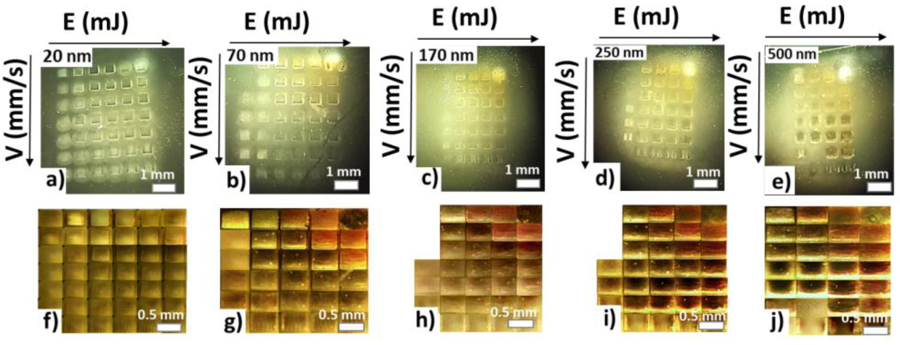
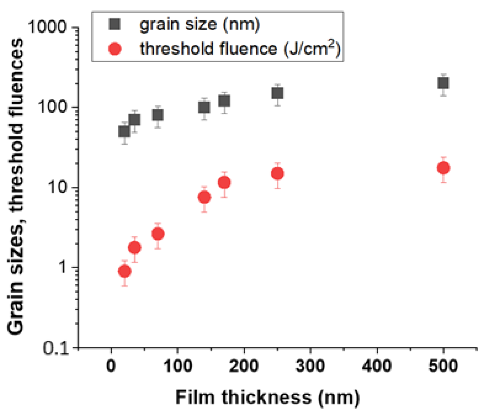
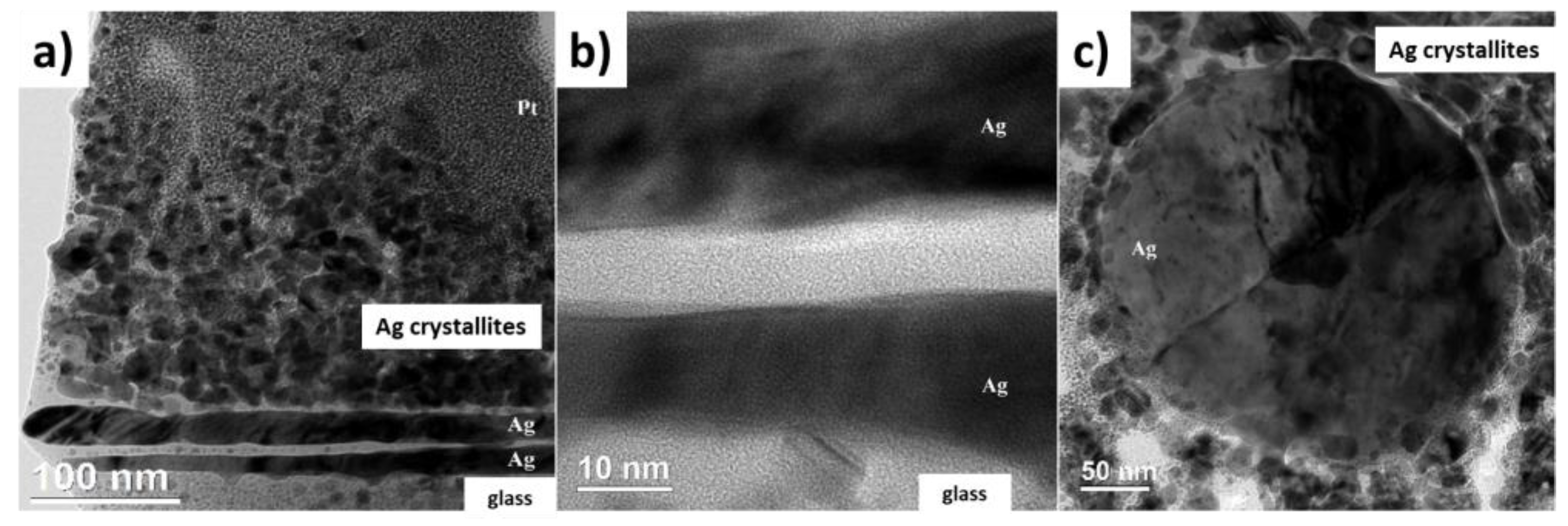
3.1. The Donor Films Characterization

The as-deposited donor silver films with thicknesses of 20, 70, 170, 250, and 500 nm, obtained by magnetron sputtering in an argon atmosphere, were studied by SEM and AFM microscopy in order to identify their surface topography and crystallinity (Figure 2). As can be seen, the surface of the donor films has a granular structure. The grain size varies depending on the film thickness.
The surface roughness (Rz) and average grain size (Figure 3; see also XRD results below) both increased with increasing film thickness. In Figure 3, the single-shot threshold ablation fluences of the films are also shown. These fluences monotonously increase versus the film thickness, potentially due to the thicker silver films having a higher thermal capacity and conductivity, which leads to the increased energy deposition depth and higher laser energy required to achieve the total removal threshold [22,23].

3.2. Visualization of Surface Topography

At a fixed laser pulse repetition rate of 20 kHz and with a 30-μm distance between the donor and acceptor substrates, laser-induced forward transfer of the different donor silver films with variable thicknesses of 20–500 nm onto a glass plate was performed for the different pulse energies E = 0.1, 0.2, 0.4, 0.6, and 0.8, 1 mJ (Figure 4, direction from left to right) and scanning speeds V = 10, 50, 100, 300, 500, 1000, and 2000 mm/s (Figure 4, direction from top to bottom). The produced arrays of the transferred spots are shown in Figure 4 at different magnifications. As can be seen, for the thicker films (thickness = 250 and 500 nm), the regions transferred at the 0.1-mJ and 0.2-mJ pulse energies are missing, indicating no LIFT process. On the other hand, at 1-mJ energy and a scanning speed of 10 mm/s, the transferred spots appear ablated for each film thickness.
The internal nanostructure of the transferred spots was studied by bright-field TEM (BF TEM) using the sample prepared from the 500-nm-thick donor film lifted-up at E = 0.4 mJ, V = 1800 mm/s (N = 2). The transferred spots have a complex structure with five characteristic layers (Figure 5). As visible in Figure 5b, alternating dense layers of different crystalline (~20 nm thick) and amorphous (~10 nm) materials are formed at the surface of the acceptor silica substrate. This structure is covered by the ~300 nm foam-like nanocrystalline layer transferred by the last laser pulse. The foam-like layer consists of nanoparticle ensembles, with the nanoparticle size varying over a range of 5–500 nm. The intermediate glass layers were formed because the substrate glass from the donor substrate was also ablatively transferred.
LIFT transfer over the 30-micron air distance is a slow process (timescale ~1 μs), compared to the 120-ns laser pulse duration, for typical matter transfer speeds of 10–100 m/s [24,25]. The sintering of opaque transferred material can be realized only by subsequent laser pulses at the same spot. Hence, accounting for the 3-pulse laser exposure per spot, one can assume the laser transfer and sintering of the foam-like transferred layer is achieved by the first two pulses, with the last one transferred without sintering. Hence, both the transfer and sintering steps could be combined in this multi-shot LIFT regime without ablation of the transferred material, resulting in nanometer-thick, continuous crystalline metallic layers.

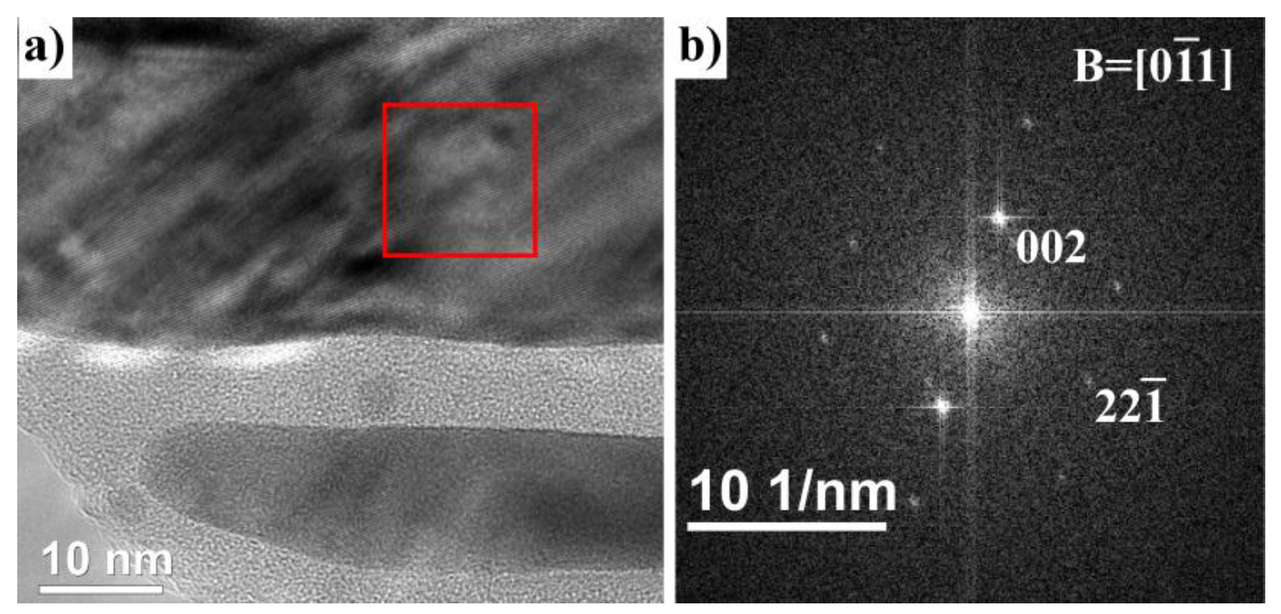
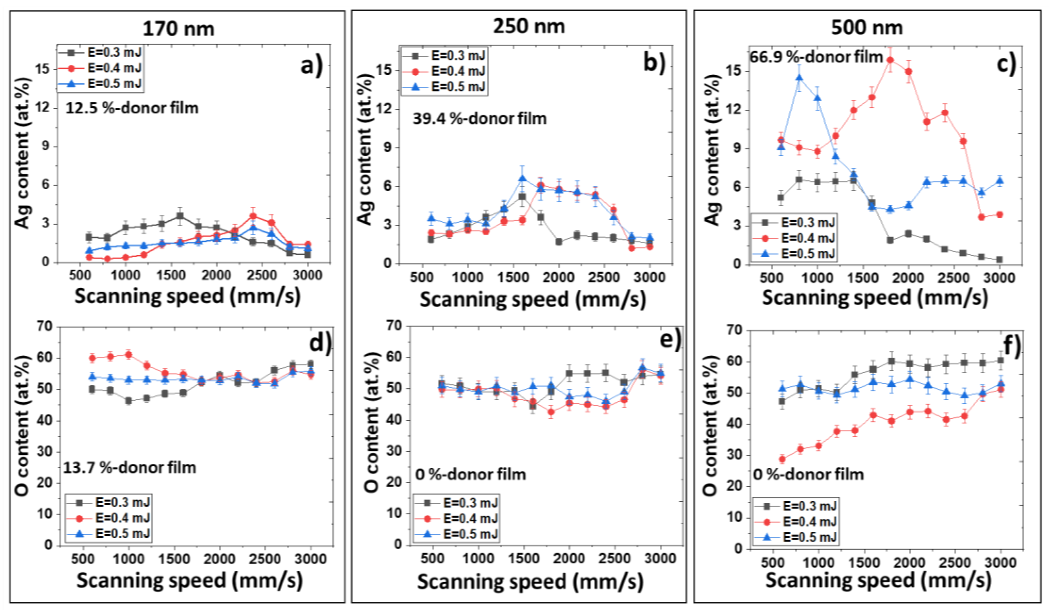
3.3. Chemical and Phase Compositions

To clarify the origin of the different layers formed inside the transferred spots, STEM-EDX compositional maps were acquired. As shown in Figure 6, STEM-EDX analysis confirms that the dense and foam-like crystalline layers contain mainly silver, while the intermediate spacing layers are the transferred silica glass (Figure 6).
The presence of oxygen inside the silver-enriched layers of the transferred spots cannot be firmly excluded by EDX analysis. Hence, the nature of these layers required more detailed verification. Therefore, a complementary high-resolution transmission electron microscopy (HRTEM) study was performed. The typical HRTEM image and corresponding Fast Fourier Transformed (FFT) pattern of the transferred silver layer clearly demonstrate that the local crystal structure fully matches the F m 3 ¯ m (225) space group of pure metallic silver (Figure 7).
The phase composition and crystallinity of the conductive silver tracks transferred at E = 0.4 mJ and V = 1000, 1800 mm/s were examined by XRD (Figure 8). Five main characteristic diffraction peaks were observed at 2θ ≈ 38.1° (111), 44.4° (200), 64.6° (220), 77.5° (311), and 82° (222), being related to the cubic silver phase, in agreement with the local SAED analysis in Figure 7. The nanocrystalline nature of the pure elemental metallic silver in the samples was revealed considering the XRD spectral linewidths [26].
The corresponding crystallite sizes (D) were evaluated by analyzing the XRD data using Scherrer’s Formula (1)
D h k l = 0.9   λ β h k l   c o s Θ
where λ = 0. 154 nm (Cu Kα-line) is the X-ray wavelength, β is the peak full linewidth at half maximum (FWHM), and θ is the diffraction angle at the (111), (200), (311), and (222) planes. For the data presented in Table 1, the average size of the crystallites was derived as ≈13–21 nm, in agreement with the sintered silver layer thickness of 10–20 nm and typical size of nanocrystallites in Figure 4.
According to our EDX elemental analysis of the entire transferred material, the content of transferred silver (Figure 9a–c) increases with increasing donor film thickness, while non-monotonously (with a maximum) varying versus scan speed (pulse exposure N). In contrast, the oxygen content weakly changes versus film thickness, pulse energy, and scan speed (Figure 9d–f), reflecting its surface oxidation origin.
The XPS survey spectrum and elemental spectra of the Si 2p, C 1s, O 1s, Ag 3d, and Ag MNN regions were additionally analyzed to envision the chemical state (bonding) of silver in the upper, foam-like part of the transferred layers. The Ag 3d region is represented by a doublet with binding energies of about 367.6 and 373.6 eV (Ag 3d5/2 and Ag 3d3/2, respectively), shifted to lower energies (relative to the characteristic peak of metallic silver) (Figure 10a). Similar results were observed in the work [27], indicating the existence of oxidized silver [28] or, possibly, the nanocrystalline character of the metal. Meanwhile, the view of the spectrum of the Ag MNN region clearly demonstrates that the silver in the upper layer is mostly in the form of metallic silver (Figure 10b).

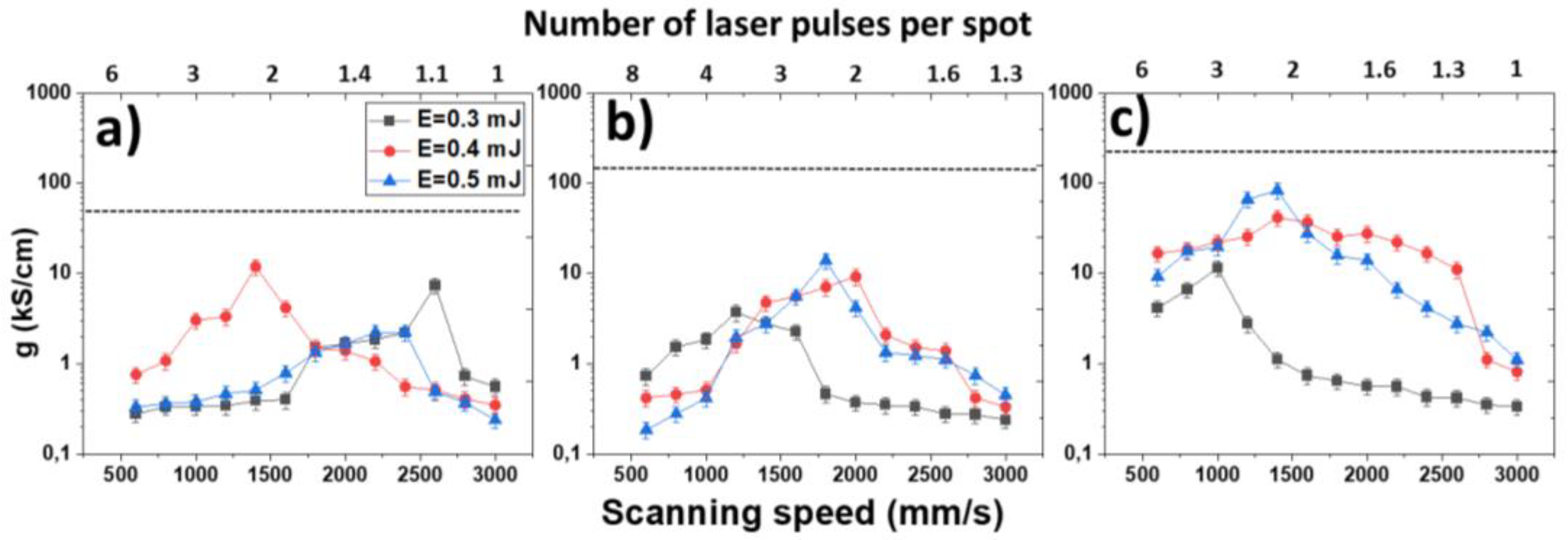
3.4. Electrophysical Properties

The specific electrical conductivity, g, of the original donor films with their thicknesses of 500, 250, and 170 nm was measured to equal 250 kS/cm, 130 kS/cm, and 65 kS/cm (Figure 11), respectively. In comparison, depending on the scanning speed and pulse energy, for the 170-nm-thick film, its transferred replica demonstrated the specific electrical conductivity magnitudes, varying from 0.23 to 12 kS/cm (Figure 11a), for 250-nm-thick film g = 0.18–14 kS/cm (Figure 11b), and for the 500-nm-thick film g = 0.33–83 kS/cm (Figure 11c).
In this case, the variation in the specific electrical conductivity of the conductive tracks occurred non-monotonously versus the scanning speed (the number of exposed pulses per spot), with the intermediate maximum of the g-value requiring more pulses (N = 2–4) for lower pulse energies (Figure 11). The optimal conductivity value was achieved for about 2–3 pulses per spot (scanning speed—1200–2400 mm/s), when particles of the donor film were transferred by the first (and second) pulse and their subsequent sintering occurred at the second (and third) pulse. As the scanning speed increased over 2400 mm/s (N < 1.5), the continuity of the resulting conductive element deteriorated, since only single-pulse transfer occurred without sintering by the missing subsequent pulses. When the scanning speed decreased below 1500 mm/s, ablative removal of the transferred material from the acceptor substrate by multiple pulses (more than 3) occurred, leading to a decrease in its specific conductivity. These trends partly resemble those for the EDX-acquired silver transfer in Figure 9, indicating the contributions of laser transfer and secondary ablative removal (re-ablation) processes. The difference between the trends in Figure 9 and Figure 11 could be assigned to the sintering process, which becomes more pronounced in Figure 11 at N ≥ 2.

4. Conclusions

In this study, we performed a very challenging multi-parametric optimization of the silver-film LIFT process in order to achieve high specific electrical conductivity of the film replica on the acceptor silica glass substrate without a second sintering step by laser or oven heating. Varying the donor silver film thickness, laser pulse energy, and scan speed at the fixed repetition rate, focusing conditions, and transfer distance, the appropriate conducting silver replicas were obtained in a single step on the silica glass acceptor substrates with the specific electrical conductivity value of ≈83 kS/cm, which is just three-fold lower than that of the corresponding as-deposited donor film, and eight-fold lower than that of bulk silver. Double or triple exposure per spot appears optimal for producing laser transfer and sintering by the consequent laser pulses in the scanning mode. Other additional chemical and structural studies indicate the continuous, purely elemental, nanocrystalline, and metallic character of the transferred/sintered silver nanolayers. As a result, fast, high-throughput, on-demand LIFT printing of highly conducting silver microelements becomes possible for the first time through the single-pass one-step procedure, paving the way for large-scale microfabrication in microelectronics.

Author Contributions

Conceptualization, S.K. and P.H.M.; formal analysis, A.G.; investigation, A.N., N.S., P.P., E.U., V.P., N.P., I.S., D.Z., P.V.D., E.K., S.S. and O.E.; writing—original draft preparation, A.N. and S.K.; writing—review and editing, P.H.M., D.K., S.S., E.U., V.P. and P.V.D.; visualization, D.K., O.E. and P.P.; supervision, S.K.; data curation, E.K. and I.S.; validation, N.S. and D.Z. All authors have read and agreed to the published version of the manuscript.

Funding

This research was supported by the Ministry of Science and Higher Education of the Russian Federation (agreement no. 075-15-2023-603).

Institutional Review Board Statement

Not applicable.

Informed Consent Statement

Not applicable.

Data Availability Statement

Supporting data can be provided upon reasonable request.

Acknowledgments

The equipment used was supplied by the Ural Center for Shared Use “Modern Nanotechnology” of Ural Federal University (Reg. no. 2968), which is supported by the Ministry of Science and Higher Education RF and of the Center for Collective Use “Structural Diagnostics of Materials” of the Federal Scientific Research Center “Crystallography and Photonics” of the Russian Academy of Sciences.

Conflicts of Interest

The authors declare no conflicts of interest.

References

  1. Pal, R.K.; Farghaly, A.A.; Collinson, M.M.; Kundu, S.C.; Yadavalli, V.K. Photolithographic micropatterning of conducting polymers on flexible silk matrices. Adv. Mater. 2016, 28, 1406–1412. [Google Scholar] [CrossRef]
  2. Peng, C.N.; Wang, C.W.; Chan, T.C.; Chang, W.Y.; Wang, Y.C.; Tsai, H.W.; Chueh, Y.L. Resistive switching of Au/ZnO/Au resistive memory: An in situ observation of conductive bridge formation. Nanoscale Res. Lett. 2012, 7, 559. [Google Scholar] [CrossRef]
  3. Wu, B.; Kumar, A. Extreme ultraviolet lithography: A review. J. Vac. Sci. Technol. B 2007, 25, 1743–1761. [Google Scholar] [CrossRef]
  4. Sopeña, P.; Fernández-Pradas, J.M.; Serra, P. Laser-induced forward transfer of low viscosity inks. Appl. Surf. Sci. 2017, 418, 530–535. [Google Scholar] [CrossRef]
  5. Wang, X.; Xu, B.; Huang, Y.; Zhang, J.; Liu, Q. Laser-induced forward transfer of silver nanoparticle ink using burst technique. Appl. Phys. A 2019, 125, 845. [Google Scholar] [CrossRef]
  6. Fernández-Pradas, J.M.; Sopeña, P.; González-Torres, S.; Arrese, J.; Cirera, A.; Serra, P. Laser-induced forward transfer for printed electronics applications. Appl. Phys. A 2018, 124, 214. [Google Scholar] [CrossRef]
  7. Khan, S.; Ali, S.; Bermark, A. Recent developments in printing flexible and wearable sensing electronics for healthcare applications. Sensors 2019, 19, 1230. [Google Scholar] [CrossRef] [PubMed]
  8. Rapp, L.; Constantinescu, C.; Larmande, Y.; Diallo, A.K.; Videlot-Ackermann, C.; Delaporte, P.; Alloncle, A.P. Functional multilayered capacitor pixels printed by picosecond laser-induced forward transfer using a smart beam shaping technique. Sens. Actuator A Phys. 2015, 224, 111–118. [Google Scholar] [CrossRef]
  9. Sones, C.L.; Kaur, K.S.; Ganguly, P.; Banks, D.P.; Ying, Y.J.; Eason, R.W.; Mailis, S. Laser-induced-forward-transfer: A rapid prototyping tool for fabrication of photonic devices. Appl. Phys. A 2010, 101, 333–338. [Google Scholar] [CrossRef]
  10. Xu, J.J. Plastic electronics and future trends in microelectronics. Synth. Met. 2000, 115, 1–3. [Google Scholar] [CrossRef]
  11. Rehman, Z.U.; Yang, F.; Wang, M.; Zhu, T. Fundamentals and advances in laser-induced transfer. Opt. Laser Technol. 2023, 160, 109065. [Google Scholar] [CrossRef]
  12. Delaporte, P.; Alloncle, A.P. Laser-induced forward transfer: A high resolution additive manufacturing technology. Opt. Laser technol. 2016, 78, 33–41. [Google Scholar] [CrossRef]
  13. Hussain, A.; Lee, H.L.; Moon, S.J. Sintering of Silver Nanoparticle Structures and the Pursuit of Minimum Resistivity. Mater. Today Commun. 2022, 34, 105159. [Google Scholar] [CrossRef]
  14. Khan, S.; Lorenzelli, L.; Dahiya, R.S. Technologies for printing sensors and electronics over large flexible substrates: A review. IEEE Sens. J. 2014, 15, 3164–3185. [Google Scholar] [CrossRef]
  15. Mathews, S.A.; Beniam, I.; Charipar, N.; Piqué, A. Laser induced forward transfer (lift) for direct-write fabrication and assembly of microelectronics. In Proceedings of the International Congress on Applications of Lasers & Electro-Optics, Orlando, FL, USA, 14–16 October 2018. [Google Scholar]
  16. Mailis, S.; Zergioti, I.; Koundourakis, G.; Ikiades, A.; Patentalaki, A.; Papakonstantinou, P.; Fotakis, C. Etching and printing of diffractive optical microstructures by a femtosecond excimer laser. Appl. Opt. 1999, 38, 2301–2308. [Google Scholar] [CrossRef]
  17. Inui, T.; Mandamparambil, R.; Araki, T.; Abbel, R.; Koga, H.; Nogi, M.; Suganuma, K. Laser-induced forward transfer of high-viscosity silver precursor ink for non-contact printed electronics. Rsc. Adv. 2015, 5, 77942–77947. [Google Scholar] [CrossRef]
  18. Makrygianni, M.; Kalpyris, I.; Boutopoulos, C.; Zergioti, I. Laser induced forward transfer of Ag nanoparticles ink deposition and characterization. Appl. Surf. Sci. 2014, 297, 40–44. [Google Scholar] [CrossRef]
  19. Song, L.; Xu, B.B.; Cheng, Q.; Wang, X.; Luo, X.; Chen, X.; Huang, Y. Instant interfacial self-assembly for homogeneous nanoparticle monolayer en-abled conformal “lift-on” thin film technology. Sci. Adv. 2021, 7, eabk2852. [Google Scholar] [CrossRef]
  20. Zacharatos, F.; Makrygianni, M.; Geremia, R.; Biver, E.; Karnakis, D.; Leyder, S.; Zergioti, I. Laser Direct Write micro-fabrication of large area electronics on flexible substrates. Appl. Surf. Sci. 2016, 374, 117–123. [Google Scholar] [CrossRef]
  21. Lim, J.; Kim, Y.; Shin, J.; Lee, Y.; Shin, W.; Qu, W.; Hong, S. Continuous-Wave Laser-Induced Transfer of Metal Nanoparticles to Arbitrary Polymer Substrates. Nanomaterials 2020, 10, 701. [Google Scholar] [CrossRef]
  22. Nastulyavichus, A.A.; Kudryashov, S.I.; Smirnov, N.A.; Rudenko, A.A.; Kharin, A.Y.; Zayarny, D.A.; Ionin, A.A. Nanosecond-laser plasma-mediated generation of colloidal solutions from silver films of variable thickness: Colloidal optical density versus pre-determined ablated mass. Opt. Laser Technol. 2019, 111, 75–80. [Google Scholar] [CrossRef]
  23. Nastulyavichus, A.; Kudryashov, S.; Tolordava, E.; Rudenko, A.; Kirilenko, D.; Gonchukov, S.; Yushina, Y. Generation of silver nanoparticles from thin films and their antibacterial properties. Laser Phys. Lett. 2022, 19, 075603. [Google Scholar] [CrossRef]
  24. Pohl, R.; Visser, C.W.; Römer, G.W.; Lohse, D.; Sun, C.; Huis, B. Ejection regimes in picosecond laser-induced forward transfer of metals. Phys. Rev. Appl. 2015, 3, 024001. [Google Scholar] [CrossRef]
  25. Feinaeugle, M.; Alloncle, A.P.; Delaporte, P.; Sones, C.L.; Eason, R.W. Time-resolved shadowgraph imaging of femtosecond laser-induced forward transfer of solid materials. Appl. Surf. Sci. 2012, 258, 8475–8483. [Google Scholar] [CrossRef]
  26. Gauri, B.; Vidya, K.; Sharada, D.; Shobha, W. Synthesis and characterization of Ag/AgO nanoparticles as alcohol sensor. Res. J. Chem. Environ. 2016, 20, 1–5. [Google Scholar]
  27. Gopiraman, M.; Deng, D.; Saravanamoorthy, S.; Chung, I.M.; Kim, I.S. Gold, silver and nickel nanoparticle anchored cellulose nanofiber composites as highly active catalysts for the rapid and selective reduction of nitrophenols in water. RSC Adv. 2018, 8, 3014–3023. [Google Scholar] [CrossRef]
  28. Prieto, P.; Nistor, V.; Nouneh, K.; Oyama, M.; Abd-Lefdil, M.; Díaz, R. XPS study of silver, nickel and bimetallic silver–nickel nanoparticles prepared by seed-mediated growth. Appl. Surf. Sci. 2012, 258, 8807–8813. [Google Scholar] [CrossRef]
Figure 1. Schematic of the experiment (F—focal lens distance, 2ω0—laser spot).
Photonics 11 00119 g001
Figure 2. SEM (ae) and AFM (fj) images of the different as-deposited donor silver films, and their corresponding 3D roughness maps (ko).
Photonics 11 00119 g002
Figure 3. Dependences of single-shot through ablation thresholds (bottom ordinate) and film grain sizes (top ordinate) on silver film thickness.
Photonics 11 00119 g003
Figure 4. Optical images of silver spots transferred in different laser regimes for film thicknesses of (a,f) 20 nm, (b,g) 70 nm, (c,h) 170 nm, (d,i) 250 nm, and (e,j) 500 nm, captured at different magnifications. The dimensions of each printed spot are 0.5 × 0.5 mm. Pulse energy and scanning speed ranges are given in the text.
Photonics 11 00119 g004
Figure 5. BF-TEM cross-section images of the sample prepared from 500-nm-thick donor film lifted-up at E = 0.4 mJ, V = 1800 mm/s (N = 2): (a) general view; (b) silver and silica layers on the acceptor surface transferred by the first and second pulses; (c) Ag nanoparticle in the foam-like layer transferred by the last pulse.
Photonics 11 00119 g005
Figure 6. STEM (a)-EDX (b) compositional maps of the sample prepared from 500-nm-thick donor film lifted-up at E = 0.4 mJ, V = 1800 mm/s (N = 2).
Photonics 11 00119 g006
Figure 7. HRTEM image of silver layer taken close to [ 0 1 ¯ 1 ] zone axis and (a) corresponding FFT pattern (b).
Photonics 11 00119 g007
Figure 8. XRD spectra of the LIFT-transferred silver layers.
Photonics 11 00119 g008
Figure 9. Dependences of EDX-derived silver (ac) and oxygen (df) content for different pulse energies as a function of scanning speed in LIFT samples for 170-, 250-, and 500-nm-thick donor films.
Photonics 11 00119 g009
Figure 10. Comparative Ag 3d5/2, Ag 3d3/2 (a,b) Ag MNN Auger XPS spectra of the upper transferred layer at scanning speeds of 2600 mm/s (2), 1800 mm/s (3), and 1000 mm/s (4) at pulse energy E = 0.5 mJ and 250 nm film thickness. The reference spectra of bulk metallic silver are marked by (1).
Photonics 11 00119 g010
Figure 11. Dependence of specific electrical conductivity g of conducting silver tracks on scanning speed (number of laser pulses per spot—top axis) at different pulse energies for the film thicknesses of 170 nm (a), 250 nm (b), and 500 nm (c). The reference dotted lines correspond to the g-values of their donor films.
Photonics 11 00119 g011
Table 1. XRD data.
Table 1. XRD data.
SampleCrystallite Size (111), nmCrystallite Size (200), nmCrystallite Size (220), nmCrystallite Size (311), nmCrystallite Size (222), nm
V = 1800 mm/s1820172120
V = 1000 mm/s16131419-
Disclaimer/Publisher’s Note: The statements, opinions and data contained in all publications are solely those of the individual author(s) and contributor(s) and not of MDPI and/or the editor(s). MDPI and/or the editor(s) disclaim responsibility for any injury to people or property resulting from any ideas, methods, instructions or products referred to in the content.

