Small Footprint and High Extinction Ratio Cladding-Modulated Bragg Grating Structure as a Wideband Bandstop Filter


Institute of Microelectronics and Optoelectronics, Warsaw University of Technology, Koszykowa 75, 00-662 Warszawa, Poland
*
Author to whom correspondence should be addressed.
Photonics 2024, 11(2), 158; https://doi.org/10.3390/photonics11020158
Submission received: 18 January 2024
/
Revised: 3 February 2024
/
Accepted: 5 February 2024
/
Published: 6 February 2024
(This article belongs to the Special Issue Advanced Photonic Sensing and Measurement II)
Abstract
:This study presents a comprehensive numerical investigation of silicon Bragg grating (BG) waveguide structures with cladding modulation. The device design features a uniform silicon ridge waveguide with corrugated cladding on both sides. Two distinct architectures are explored: one where silicon serves as the cladding and another where gold (Au) is employed. Our detailed analysis uncovers compelling results for both configurations. The silicon corrugated cladding BG waveguide demonstrates a bandstop bandwidth of ~50 nm, accompanied by an extinction ratio (ER) of 7.98 dB. The device footprint is compact, measuring approximately 16.4 × 3 µm2. In contrast, the Au corrugated cladding BG waveguide exhibits exceptional performance, boasting a wideband bandstop bandwidth of ~143 nm and an impressive ER of 19.96 dB. Despite this enhanced functionality, the device maintains a reasonably small footprint at around 16.9 × 3 µm2. This investigation underscores the potential of Au corrugated cladding BG waveguides as ideal candidates for achieving high-spectral-characteristic bandstop filters. The significant improvement in bandstop bandwidth and ER makes them promising for advanced optical filtering applications.
1. Introduction
Bragg grating (BG) waveguides stand as a pivotal breakthrough in integrated optics, offering a remarkably adaptable foundation for manipulating and governing light within the intricate landscape of photonic circuits [1]. These waveguides ingeniously leverage the principle of Bragg scattering, orchestrating periodic variations in the refractive index to craft a grating structure that induces wavelength-selective reflection or transmission [2,3]. The rhythmic modulation inherent in the waveguide’s properties grants an exquisite degree of control over light propagation, unleashing the potential for crafting precision-engineered optical filters, modulators, and couplers [4,5]. The far-reaching impact of BG waveguides extends into the telecommunications domain, where they play an indispensable role in advancing wavelength division multiplexing (WDM) systems [6,7]. This contribution enables the concurrent transmission of multiple data streams across a single optical fiber. Beyond telecommunications, these waveguides find application in sensing realms, including refractive index, temperature, and strain measurements, leveraging the wavelength shift induced by fluctuations in the surrounding environment [8,9,10,11]. The ever-expanding versatility of BG waveguides serves as a driving force behind continuous innovations in optical communication [12] and sensing technologies [13,14,15].
The cladding-modulated BG waveguide stands as a pioneering advancement in the field of integrated optics, departing from the conventional structure of a core material enveloped by cladding layers [16,17,18]. In this innovative strategy, deliberate modulation of the cladding refractive index along the waveguide’s length introduces a novel mechanism for precisely manipulating light within its confines [19,20]. As light traverses the waveguide, the orchestrated cladding modulation dynamically interacts with the core, exerting an influence on the effective refractive index experienced by guided modes. This intricate interplay engenders dynamic changes in the effective index, bestowing precise control over the Bragg condition and, consequently, the reflective properties of the grating [20]. This design innovation underscores the perpetual evolution of BG waveguides, highlighting their adaptability in addressing a myriad of optical engineering challenges [21].
In [20], a photonic biosensor featuring a grating waveguide with cladding modulation, composed of three channels on a silicon-on-insulator (SOI) platform, is proposed. The optical mode propagates in the central channel, while the remaining two channels engage with the lateral field. Gratings are specifically crafted in the outer channels, and their parameters are fine-tuned to achieve a narrow stopband in the transmission spectra. Furthermore, in [19], cladding-modulated BG on an SOI platform is presented. The grating is achieved through the periodic placement of cylinders along a waveguide, allowing for variation in coupling strength by adjusting the distance between the cylinders and the waveguide. This implementation provides precise control and a broad dynamic range of coupling strengths and bandwidths, catering to specific application requirements. The modeling results are experimentally validated, demonstrating significant differences in coupling strengths (43 and 921 per cm) with corresponding bandwidths of 8 and 16 nm, respectively. Whereas, in this work, we numerically investigated two types of cladding-modulated BG waveguide structures: one with silicon corrugated cladding and the other with gold (Au) corrugated cladding, which are further compared to determine the best spectral characteristics. The numerical analysis of the devices is performed via the finite element method (FEM). The spectral characteristics and footprint of both grating structures are compared and provide a guideline for the design of a highly efficient BG wideband bandstop filter.
2. Working Principles of BG Structure and Numerical Model
The operational principle of BG waveguides hinges on the fundamental concept of Bragg scattering, an intricate phenomenon arising from the systematic modulation of the refractive index within the waveguide architecture. Typically comprised of a core material enveloped by cladding layers, these waveguides exhibit a carefully engineered periodic variation in the refractive index, giving rise to a grating structure that spans the length of the waveguide. For a single-mode waveguide, the effective index (neff) can be expressed as follows:
where neff is the effective index of the guided mode, n0 is the refractive index of the core material, and Δn is the refractive index modulation. As light traverses through the waveguide, the periodic alterations in the refractive index induce constructive interference, specifically for wavelengths that satisfy the Bragg condition. This constructive interference orchestrates the reflection of these wavelengths, effectively shaping a wavelength-selective mirror within the structure of the waveguide. The reflected wavelength (λBragg) is known as the Bragg wavelength, which is expressed as follows:
where Λ is the grating period. The precise determination of the spacing in the periodic structure dictates the reflected wavelength, thereby affording meticulous control over which wavelengths are either reflected or transmitted. This unique capability positions BG waveguides as pivotal components, offering unparalleled precision in the manipulation of light for diverse applications, ranging from optical filters to modulators.
neff = n0 + Δn;
λBragg = 2 × neff × Λ;
The FEM stands for a robust numerical approach extensively applied in engineering and scientific simulations. FEM discretizes intricate physical systems into smaller, finite elements, enabling the approximation of solutions to partial differential equations. COMSOL Multiphysics, serving as a versatile simulation platform, excels in implementing FEM across a diverse range of multiphysics phenomena, encompassing heat transfer, fluid dynamics, electromagnetics, and structural mechanics [22]. To ensure computationally feasible simulation results with the available computing resources, the subdomains within the proposed device undergo subdivision into triangular mesh elements with a grid size of λ/50 for a more realistic representation. The introduction of scattering boundary conditions (SBCs) to the outer boundaries of the FEM simulation window effectively signifies open geometry. While previous studies on plasmonic devices predominantly relied on 2D numerical simulations, treating one dimension as infinitely long, this study expedites the evaluation of device performance in such simulations, minimizing loss [13,23]. However, it is crucial to note that the system’s loss is notably influenced by the height of the waveguide structure, a vital consideration in real-world processing [24].
3. Cladding-Modulated BG Waveguide Designs and Optimization Process
The first BG waveguide design consisted of a silicon ridge waveguide surrounded on both sides by a silicon corrugated cladding, as illustrated in Figure 1a. This configuration imparts neff modulation to the guided mode. The width of the silicon waveguide is denoted as “WSi”, and the depth of the corrugation is represented as “d”. The corrugation period, denoted as “Λ”, is equal to the sum of “a” and “b”, where “a” and “b” correspond to the unetched and etched segments, respectively. The separation between the silicon waveguide and the corrugated cladding is defined as “g”. The number of corrugation periods is labeled “N”.
In the case of the Au cladding-modulated BG waveguide structure, the silicon waveguide follows the standard ridge waveguide design and is enclosed between corrugated metallic cladding layers on both sides. A small gap between the silicon waveguide and the metallic corrugated cladding resulted in a hybrid plasmonic waveguide structure [25,26], as depicted in Figure 1b. Mode propagation in hybrid plasmonic waveguides involves the guided transmission of plasmonic modes along structures that combine multiple materials with distinct plasmonic properties. These waveguides typically consist of a metal-dielectric hybrid configuration, where the metal component supports the propagation of surface plasmon polaritons (SPPs), while the dielectric component helps confine and guide the plasmonic modes. The interaction between the metal and dielectric material in a hybrid plasmonic waveguide allows for the manipulation and control of the guided modes, influencing factors such as mode confinement, propagation length, and dispersion characteristics. To ensure a comprehensive and equitable analysis of the BG structures, comparable geometric parameters are maintained. The detailed geometric parameters of the device employed in this study are elucidated in Table 1.
The graphically represented E-field distribution and effective refractive index in BG structure at 1550 nm are illustrated for three distinct scenarios: a noncorrugated silicon core waveguide (depicted in Figure 2a), a silicon core waveguide with silicon cladding on both sides (depicted in Figure 2b–e), and a silicon core waveguide with gold Au cladding on both sides (shown in Figure 2f–i) for g ranges between 20 nm and 50 nm. The effective index modulation is the change in the average refractive index within the grating region, influencing the dispersion and guiding properties of the waveguide. By carefully engineering this modulation, desired spectral responses and the optimized performance of BG waveguides for specific applications, such as wavelength filtering, dispersion compensation, and signal processing in optical communication systems, are achieved. The ∆neff (effective index of the noncorrugated cladding segment—effective index of the corrugated cladding segment) of the silicon corrugated cladding BG waveguide decreases from 0.2295 to 0.1058 as g increases from 20 nm to 50 nm (described in Table 2). In the case of the Au corrugated cladding BG waveguide, the ∆neff decreases from 0.3617 to 0.1582 as g increases from 20 nm to 50 nm (see Table 2). This signifies that the effective refractive index modulation achieved with Au cladding is significantly greater than that achieved with silicon cladding. This underscores the enhanced performance and unique characteristics offered by Au cladding in comparison to silicon cladding, which is further proved with our numerical analysis.
3.1. Silicon Corrugated Cladding BG Waveguide Structure
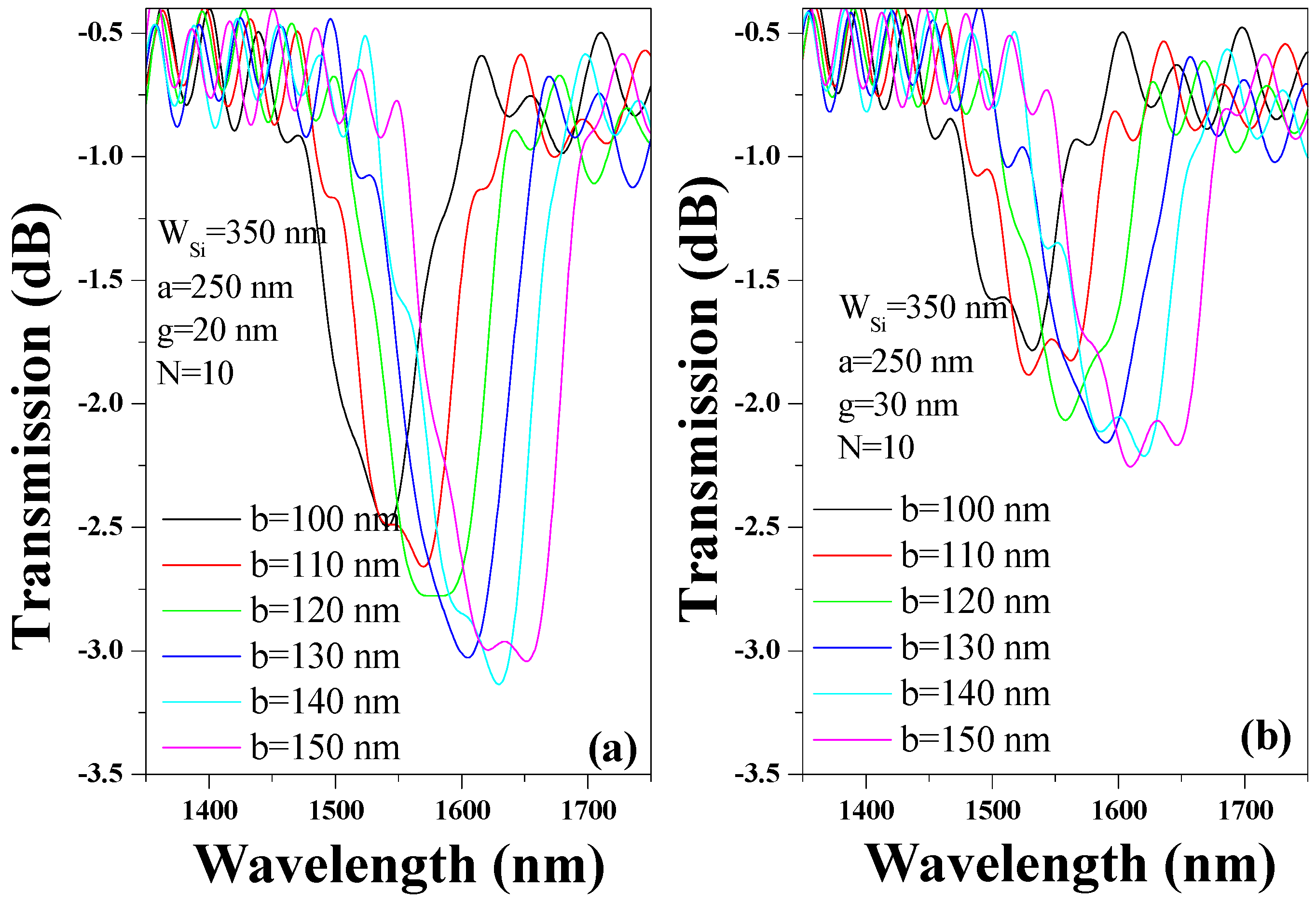
The grating Λ, represented by the sum (a + b), and the gap (g) between the silicon waveguide core and the silicon corrugated cladding play a pivotal role in shaping the effective index modulation of the mode propagating within the waveguide. In our preliminary analysis, we maintain WSi, a, and N at fixed values of 350 nm, 250 nm, and 10, respectively. To enhance the spectral characteristics of the silicon cladding-modulated BG waveguide, we systematically vary g, exploring values of 20 nm and 30 nm for different Λ of the grating, as illustrated in Figure 3a and Figure 3b, respectively. Observing Figure 3, it becomes evident that, with an increase in b from 100 nm to 150 nm, the bandstop undergoes a discernible redshift, accompanied by a marginal rise in the ER, which is calculated as [27]:
where Pout and Pin are the output and input power, respectively. It is crucial to emphasize that the ER experiences a reduction as g increases from 20 nm to 30 nm. Hence, caution is advised against further elevating the value of g, as this could potentially lead to a decline in the ER within the bandstop region.
ER = 10 × log (Pout/Pin);
Moreover, the impact of the silicon waveguide width on the bandstop spectrum is explored by varying WSi within the range of 350 nm to 400 nm, as illustrated in Figure 4a. Other geometric parameters—including a, b, g, and N—are held constant at 250 nm, 100 nm, 20 nm, and 10, respectively. An augmentation in WSi results in an increase in the effective index of the mode, leading to a noticeable redshift in the bandstop spectrum. This observation suggests that the range of the bandstop spectrum can be finely tuned by manipulating both the grating Λ and the width of the silicon waveguide. Ultimately, the ER of the bandstop experiences a substantial enhancement, progressing from 1.11 dB to 7.98 dB, by increasing the number (N) of grating Λ from 5 to 25, as depicted in Figure 4b. This underscores the significance of adjusting WSi, g, Λ, and N to collectively achieve the desired spectral characteristics for the BG bandstop filter [28].
The normalized H-field distribution within the silicon cladding in the modulated BG waveguide structure is illustrated in Figure 5. This depiction captures both the bandstop region and the bandpass region. Figure 5 highlights the distinct behavior of electromagnetic waves under the influence of the BG structure. In Figure 5a, the conditions align to satisfy the Bragg condition, resulting in the prevention of the electromagnetic wave from traversing through the BG structure at a specific wavelength of 1528 nm. This is a characteristic of the bandstop region, where the waves are effectively blocked. Conversely, in the bandpass region, represented in Figure 5b, the electromagnetic wave is permitted to traverse the BG structure at a different wavelength of 1602 nm. This showcases the dynamic modulation of the BG waveguide structure, allowing the passage of light in this specific wavelength range. These findings highlight the tunable and selective properties of the BG waveguide structure, offering controlled transmission and blocking capabilities based on the wavelength of the incident electromagnetic wave.
3.2. Au Corrugated Cladding BG Waveguide Structure
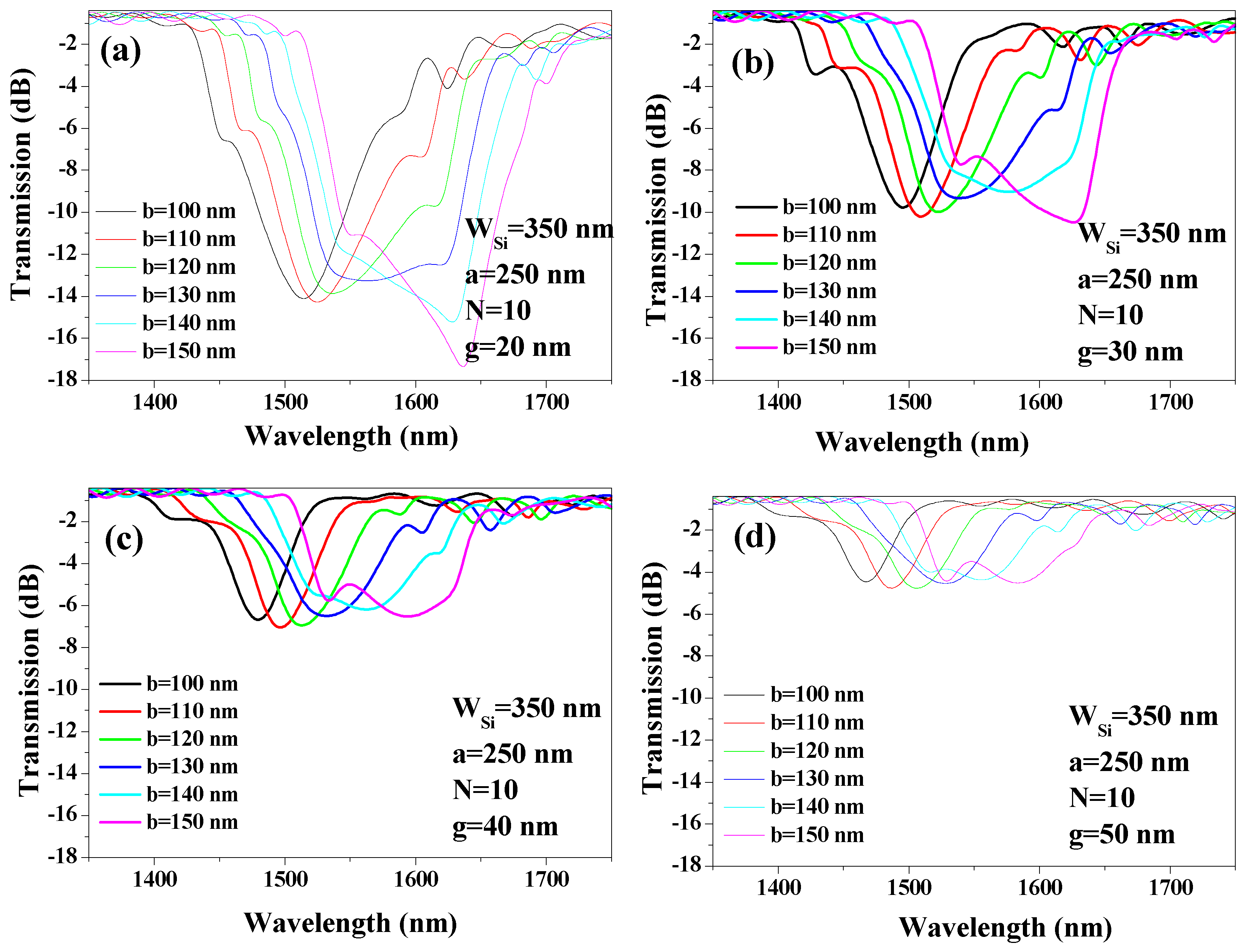
Table 2 reveals that the modulation of Au corrugated cladding results in a ∆neff range of 0.1582 to 0.3617 for g values spanning 20 nm to 50 nm. Notably, these values surpass those achieved with a silicon corrugated cladding BG structure. To gain further insights, we plotted a transmission spectrum for varying grating Λ against g, elucidating the ER of the bandstop spectrum, as illustrated in Figure 6a–d. As the grating Λ increases from 350 nm (a + b = 100 nm + 250 nm) to 400 nm (a + b = 150 nm + 250 nm), the bandstop spectrum undergoes a redshift with a subtle broadening in the bandstop bandwidth. Intriguingly, g exhibits an inverse correlation with the ER of the bandstop spectrum. This behavior is attributed to the reduction in ∆neff from 0.3617 to 0.1582 as g varies from 20 nm to 50 nm. Consequently, it is recommended to maintain the proximity of the Au corrugated cladding to the waveguide core. Alternatively, increasing N proves effective in augmenting the ER of the device, albeit at the cost of expanding the footprint of the BG filter.
The investigation meticulously scrutinizes the impact of varying the width of the silicon waveguide on the bandstop spectrum, focusing on the WSi parameter within the range of 350 nm to 400 nm, as illustrated in Figure 7a. The study maintains a constant set of geometric parameters—namely, a, b, g, and N—set at 250 nm, 110 nm, 20 nm, and 10, respectively. Remarkably, the λBragg undergoes a discernible redshift in response to a subtle reduction in the effective refractive index as WSi extends from 350 nm to 400 nm. This phenomenon is attributed to the increased effective refractive index of the propagating mode. Importantly, it is noteworthy that the shift in the bandstop spectrum is more pronounced compared to the shift observed in the silicon corrugated cladding BG waveguide configuration due to the highly sensitive nature of the hybrid mode, as depicted in Figure 4a. This observation suggests that alterations in the width of the silicon waveguide exert a more substantial influence in the form of a redshift on the bandstop spectrum than those observed in the silicon corrugated cladding BG waveguide configuration. Therefore, a bandstop filter based on this configuration can be designed for a large range of wavelength spectra.
From Figure 7b, it can be seen that by increasing N of the grating Λ from 5 to 25, the ER of the bandstop region increases from 5.1 dB to 19.96 dB, resulting in a pronounced bandstop bandwidth of ~143 nm. The characteristics offered by this BG architecture surpass the ER, bandstop bandwidth, and footprint of the one studied in Section 3.1.
The normalized H-field distribution within the Au cladding of the modulated BG waveguide structure is vividly presented in Figure 8. This visual representation encapsulates both the bandstop and bandpass regions, unraveling the intricate behavior of electromagnetic waves influenced by the BG structure. Figure 8 adeptly delineates the distinctive responses of electromagnetic waves within the BG waveguide structure. In Figure 8a, a precise alignment of conditions satisfies the Bragg condition, resulting in the prevention of electromagnetic wave propagation through the BG structure at a specific wavelength of 1523 nm. This phenomenon characterizes the bandstop region, displaying the effective blocking of waves at this specific wavelength. Conversely, the bandpass region, illustrated in Figure 8b, reveals a different scenario. Here, the electromagnetic wave is granted passage through the BG structure at a distinct wavelength of 1700 nm. This dynamic modulation of the BG waveguide structure enables the controlled transmission of light within this specific wavelength range. The spectral characteristics of silicon cladding-modulated BG structure and Au cladding-modulated BG structure are tabulated in Table 3.
4. Proposed Fabrication Procedure
The fabrication of the cladding-modulated BG waveguide involves a two-step process. Initially, an SOI wafer is spin-coated with a photoresist or electron beam resist, and a deep ultraviolet (DUV) photolithography or electron beam lithography (EBL) process can be employed to transfer a waveguide pattern onto the resist [29]. Removing an exposed resist via developer is a crucial step in the photolithography process, playing a pivotal role in defining patterns on a substrate. After exposure to light through a mask, the resist undergoes a chemical change in the exposed regions, becoming more soluble. The developer solution selectively dissolves the exposed resist, revealing the desired pattern on the substrate. This process is essential for creating intricate and precise structures in microfabrication, semiconductor manufacturing, and other nanotechnology applications. Proper control of the development time, temperature, and concentration is vital to achieving the desired pattern fidelity and ensuring the success of subsequent processing steps in the fabrication of microdevices and integrated circuits. Subsequently, a reactive ion etching (RIE) process is applied to etch the silicon ridge waveguide into the wafer [30]. RIE holds significant importance in the realm of microfabrication and semiconductor manufacturing. This dry etching technique excels in precision and selectivity, allowing for the highly controlled removal of materials from a substrate. RIE utilizes a low-pressure plasma environment where reactive gases chemically react with the substrate’s surface, leading to efficient material removal. Its ability to achieve fine features, high anisotropy, and minimal undercutting makes RIE essential in creating intricate patterns and structures on semiconductors and microdevices. Following the formation of the silicon core, a layer of Au with the same thickness as the silicon core is deposited on the sample. Several techniques can be employed for Au deposition, each offering unique advantages. Physical vapor deposition (PVD), including techniques like sputtering and evaporation, involves the direct transition of Au from a solid source to a vapor phase, creating a thin film on the substrate. Chemical vapor deposition (CVD) allows for the controlled growth of gold layers through the chemical reactions of volatile precursors. A second lithographic process is then executed to define patterns for corrugated Au cladding. Subsequently, a chemical etching step is performed to remove the unwanted Au layer, resulting in the desired cladding-modulated structure. A comprehensive overview of this anticipated device fabrication process is presented in Figure 9 for detailed reference.
5. Conclusions
In this study, we present two distinctive architectures of cladding-modulated silicon BG waveguides tailored for filtering applications in the near-infrared (NIR) spectrum. The first configuration features a silicon ridge waveguide surrounded by corrugated silicon cladding on both sides. In contrast, the second configuration employs Au corrugated cladding around the silicon waveguide. The spectral characteristics of these BG waveguide structures are meticulously examined through numerical analysis utilizing the finite element method. In the initial design, the bandstop bandwidth, ER, and footprint of the silicon ridge waveguide surrounded by silicon corrugated cladding are determined to be 50 nm, 7.98 dB, and 16.4 × 3 µm2, respectively. Conversely, in the second configuration with Au corrugated cladding, the BG segment serves as a hybrid plasmonic waveguide. This design achieves high index modulation between dielectric and hybrid plasmonic modes, resulting in significantly superior spectral characteristics. For the hybrid plasmonic waveguide, the bandstop bandwidth is calculated at 143 nm, with an impressive ER of 19.96 dB and a footprint of 16.9 × 3 µm2. It is important to note that the presented characteristics can be further enhanced by increasing the number of periods of the filter, thereby achieving a higher ER. However, this enhancement comes at the expense of a larger footprint. This research underscores the potential for optimizing the trade-off between filter performance and device size to meet specific application requirements.
Author Contributions
Conceptualization, M.A.B.; methodology, M.A.B.; software, M.A.B.; validation, M.A.B. and R.P.; formal analysis, M.A.B.; investigation, M.A.B.; resources, R.P.; data curation, M.A.B.; writing—original draft preparation, M.A.B.; writing—review and editing, M.A.B. and R.P.; visualization, R.P.; supervision, R.P.; project administration, M.A.B.; funding acquisition, M.A.B. All authors have read and agreed to the published version of the manuscript.
Funding
This research received no external funding.
Institutional Review Board Statement
Not applicable.
Informed Consent Statement
Not applicable.
Data Availability Statement
Data are contained within the article.
Acknowledgments
The authors thank the Institute of Microelectronics and Optoelectronics, Warsaw University of Technology, for their constant support in the completion of this work.
Conflicts of Interest
The authors declare no conflicts of interest.
References
- Kaushal, S.; Cheng, R.; Ma, M.; Mistry, A.; Burla, M.; Chrostowski, L.; Azaña, J. Optical signal processing based on silicon photonics waveguide Bragg gratings: Review. Front. Optoelectron. 2018, 11, 163–188. [Google Scholar] [CrossRef]
- Burla, M.; Cortés, L.R.; Li, M.; Wang, X.; Chrostowski, L.; Azaña, J. Integrated waveguide Bragg gratings for microwave photonics signal processing. Opt. Express 2013, 21, 25120–25147. [Google Scholar] [CrossRef] [PubMed]
- Ams, M.; Dekker, P.; Gross, S.; Withford, M.J. Fabricating waveguide Bragg gratings (WBGs) in bulk materials using ultrashort laser pulses. Nanophotonics 2017, 6, 743–763. [Google Scholar] [CrossRef]
- Dual Phase-Shift Bragg Grating Silicon Photonic Modulator Operating up to 60 Gb/s. Available online: https://opg.optica.org/oe/fulltext.cfm?uri=oe-24-3-2413&id=335910 (accessed on 23 November 2023).
- Shi, W.; Veerasubramanian, V.; Plant, D.V.; Jaeger, N.A.F.; Chrostowski, L. Silicon photonic Bragg-grating couplers for optical communications. In Next-Generation Optical Networks for Data Centers and Short-Reach Links; SPIE: Washington, DC, USA, 2014; pp. 63–74. [Google Scholar] [CrossRef]
- Zhang, W.; Yao, J. A fully reconfigurable waveguide Bragg grating for programmable photonic signal processing. Nat. Commun. 2018, 9, 1. [Google Scholar] [CrossRef] [PubMed]
- Khonina, S.N.; Kazanskiy, N.L.; Butt, M.A.; Karpeev, S.V. Optical Multiplexing Techniques and Their Marriage for on-Chip and Optical Fiber Communication: A Review. Opto-Electron. Adv. 2022, 5, 210127. [Google Scholar] [CrossRef]
- Butt, M.A.; Kazanskiy, N.L.; Khonina, S.N. Advances in Waveguide Bragg Grating Structures, Platforms, and Applications: An Up-to-Date Appraisal. Biosensors 2022, 12, 497. [Google Scholar] [CrossRef] [PubMed]
- Klimov, N.N.; Mittal, S.; Berger, M.; Ahmed, Z. On-chip silicon waveguide Bragg grating photonic temperature sensor. Opt. Lett. 2015, 40, 3934–3936. [Google Scholar] [CrossRef] [PubMed]
- Missinne, J.; Teigell Benéitez, N.; Mattelin, M.-A.; Lamberti, A.; Luyckx, G.; Van Paepegem, W.; Van Steenberge, G. Bragg-Grating-Based Photonic Strain and Temperature Sensor Foils Realized Using Imprinting and Operating at Very Near Infrared Wavelengths. Sensors 2018, 18, 2717. [Google Scholar] [CrossRef]
- Sherman, S.; Zappe, H. Printable Bragg Gratings for Polymer-based Temperature Sensors. Procedia Technol. 2014, 15, 702–709. [Google Scholar] [CrossRef]
- Yao, J.; Zhang, W. Fully Reconfigurable Waveguide Bragg Gratings for Programmable Photonic Signal Processing. J. Light. Technol. 2020, 38, 202–214. [Google Scholar] [CrossRef]
- Butt, M.; Khonina, S.; Kazanskiy, N. A compact design of a modified Bragg grating filter based on a metal-insulator-metal waveguide for filtering and temperature sensing applications. Optik 2022, 251, 168466. [Google Scholar] [CrossRef]
- Li, H.; Zhu, Z.; Meng, W.; Cao, L.; Wang, Y.; Lin, Z.; Li, E.; Prades, J.D. Silicon-photonics-based waveguide Bragg grating sensor for blood glucose monitoring. Opt. Express 2022, 30, 41554–41566. [Google Scholar] [CrossRef]
- Missinne, J.; Vasiliev, A.; Elmogi, A.; Beneitez, N.T.; Bosman, E.; Van Hoe, B.; Van Steenberge, G. Bragg Grating Sensors in Laser-written Single Mode Polymer Waveguides. Procedia Eng. 2015, 120, 878–881. [Google Scholar] [CrossRef]
- Tan, D.T.H.; Ikeda, K.; Fainman, Y. Cladding-modulated bragg gratings in silicon waveguides. In Proceedings of the 2009 Conference on Lasers and Electro-Optics and 2009 Conference on Quantum Electronics and Laser Science Conference, Baltimore, MD, USA, 2–4 June 2009; pp. 1–2. [Google Scholar] [CrossRef]
- Yoon, J.; Kim, J.-Y.; Kim, J.; Hong, S.; Neseli, B.; Park, J.; Park, H.-H.; Kurt, H. Cladding modulated silicon waveguide Bragg grating with TM-polarized light for optical true time delay line. Appl. Phys. Lett. 2023, 123, 191106. [Google Scholar] [CrossRef]
- Pereira-Martín, D.; Luque-González, J.M.; Wangüemert-Pérez, J.G.; Hadij-ElHouati, A.; Molina-Fernández, Í.; Cheben, P.; Schmid, J.H.; Wang, S.; Ye, W.N.; Čtyroký, J.; et al. Complex spectral filters in silicon waveguides based on cladding-modulated Bragg gratings. Opt. Express 2021, 29, 15867–15881. [Google Scholar] [CrossRef]
- Tan, D.T.H.; Ikeda, K.; Fainman, Y. Cladding-modulated Bragg gratings in silicon waveguides. Opt. Lett. 2009, 34, 1357–1359. [Google Scholar] [CrossRef] [PubMed]
- Sahu, S.; Ali, J.; Yupapin, P.P.; Singh, G. Optical biosensor based on a cladding modulated grating waveguide. Optik 2018, 166, 103–109. [Google Scholar] [CrossRef]
- Zhang, M.; Liu, J.; Cheng, W.; Cheng, J.; Zheng, Z. A Tunable Optical Bragg Grating Filter Based on the Droplet Sagging Effect on a Superhydrophobic Nanopillar Array. Sensors 2019, 19, 3324. [Google Scholar] [CrossRef] [PubMed]
- COMSOL. COMSOL: Multiphysics Software for Optimizing Designs. Available online: https://www.comsol.com/ (accessed on 26 September 2023).
- Dhavamani, V.; Chakraborty, S.; Ramya, S.; Nand, S. Design and Simulation of Waveguide Bragg Grating based Temperature Sensor in COMSOL. J. Phys. Conf. Ser. 2022, 2161, 012047. [Google Scholar] [CrossRef]
- Butt, M.; Kazanskiy, N.; Khonina, S. Tapered waveguide mode converters for metal-insulator-metal waveguide plasmonic sensors. Measurement 2023, 211, 112601. [Google Scholar] [CrossRef]
- Okamoto, H.; Kamada, S.; Haraguchi, M.; Okamoto, T. Design of a hybrid plasmonic waveguide device using a trench structure. J. Phys. Commun. 2020, 4, 095022. [Google Scholar] [CrossRef]
- Butt, M.A.; Piramidowicz, R. Standard slot waveguide and double hybrid plasmonic waveguide configurations for enhanced evanescent field absorption methane gas sensing. Photonics Lett. Pol. 2022, 14, 1. [Google Scholar] [CrossRef]
- Klitis, C.; Cantarella, G.; Strain, M.J.; Sorel, M. High-extinction-ratio TE/TM selective Bragg grating filters on silicon-on-insulator. Opt. Lett. 2017, 42, 3040–3043. [Google Scholar] [CrossRef] [PubMed]
- Butt, M.A. Numerical investigation of a small footprint plasmonic Bragg grating structure with a high extinction ratio. Photonics Lett. Pol. 2020, 12, 3. [Google Scholar] [CrossRef]
- Butt, M.A. Integrated Optics: Platforms and Fabrication Methods. Encyclopedia 2023, 3, 824–838. [Google Scholar] [CrossRef]
- Zheng, Y.; Gao, P.; Jiang, L.; Kai, X.; Duan, J. Surface Morphology of Silicon Waveguide after Reactive Ion Etching (RIE). Coatings 2019, 9, 478. [Google Scholar] [CrossRef]
Figure 1.
Graphical interpretation of (a) standard BG waveguide and (b) cladding-modulated hybrid plasmonic BG waveguide.
Figure 1.
Graphical interpretation of (a) standard BG waveguide and (b) cladding-modulated hybrid plasmonic BG waveguide.

Figure 2.
Normalized E-field distribution in the waveguide at λ = 1550 nm; (a) silicon core (WSi = 350 nm, HSi = 300 nm); (b–e) silicon cladding on both sides of the silicon core (WSi = 350 nm, HSi = 300 nm), with g = 20 nm, 30 nm, 40 nm, and 50 nm; and (f–i) Au cladding on both sides of the silicon core (WSi = 350 nm, HSi = 300 nm) with g = 20 nm, 30 nm, 40 nm, and 50 nm. The neff values for the silicon core and the cladding corrugated core are shown in the figure.

Figure 3.
Transmission spectrum of a silicon cladding-modulated BG waveguide with different periods versus (a) g = 20 nm and (b) g = 30 nm.
Figure 3.
Transmission spectrum of a silicon cladding-modulated BG waveguide with different periods versus (a) g = 20 nm and (b) g = 30 nm.

Figure 4.
Transmission spectrum of a silicon cladding-modulated BG waveguide versus (a) WSi and (b) N.
Figure 4.
Transmission spectrum of a silicon cladding-modulated BG waveguide versus (a) WSi and (b) N.

Figure 5.
Normalized H-field distribution in the BG structure at (a) λ = 1528 nm and (b) λ = 1602 nm. The device has the following parameters: WSi = 350 nm, g = 20 nm, a = 250 nm, b = 100 nm, and N = 25.
Figure 5.
Normalized H-field distribution in the BG structure at (a) λ = 1528 nm and (b) λ = 1602 nm. The device has the following parameters: WSi = 350 nm, g = 20 nm, a = 250 nm, b = 100 nm, and N = 25.

Figure 6.
Transmission spectrum of Au cladding-modulated BG waveguide with different periods versus (a) g = 20 nm, (b) g = 30 nm, (c) g = 40 nm, and (d) g = 50 nm.
Figure 6.
Transmission spectrum of Au cladding-modulated BG waveguide with different periods versus (a) g = 20 nm, (b) g = 30 nm, (c) g = 40 nm, and (d) g = 50 nm.

Figure 7.
Transmission spectrum of an Au cladding-modulated BG waveguide versus (a) WSi and (b) N.

Figure 8.
Normalized H-field distribution in the BG structure at (a) λ = 1523 nm, (b) λ = 1700 nm. The device has the following parameters: WSi = 350 nm, g = 20 nm, a = 250 nm, b = 100 nm, and N = 25.
Figure 8.
Normalized H-field distribution in the BG structure at (a) λ = 1523 nm, (b) λ = 1700 nm. The device has the following parameters: WSi = 350 nm, g = 20 nm, a = 250 nm, b = 100 nm, and N = 25.

Figure 9.
Anticipated fabrication procedure.


Table 1.
Geometric parameters of the BG waveguide structures used in this study.
| Variable | Value | Expression |
|---|---|---|
| WSi | from 350 nm to 400 nm | Width of a silicon waveguide |
| a | 250 nm | Length of the unetched segment |
| b | from 100 nm to 150 nm | Length of the etched segment |
| d | 100 nm | Depth of corrugation |
| N | 5, 10, 15, 20, and 25 | Number of periods |
| g | 10, 20,30, and 40 nm | Gap between silicon waveguide and corrugated cladding |
Table 2.
∆neff in silicon corrugated cladding and Au corrugated cladding versus g.
| g = 20 nm | g = 30 nm | g = 40 nm | g = 50 nm | |
|---|---|---|---|---|
| ∆neff in Silicon corrugated cladding | 0.2295 | 0.1722 | 0.1335 | 0.1058 |
| ∆neff in Au corrugated cladding | 0.3617 | 0.2636 | 0.2011 | 0.1582 |
Table 3.
Spectral characteristics of silicon cladding-modulated BG structure and Au cladding-modulated BG structure.
Table 3.
Spectral characteristics of silicon cladding-modulated BG structure and Au cladding-modulated BG structure.
| Silicon Corrugated Cladding | Au Corrugated Cladding | |||||
|---|---|---|---|---|---|---|
| N | Footprint (µm)2 | Maximum ER (dB) | Bandstop Bandwidth (nm) | Footprint (µm)2 | Maximum ER (dB) | Bandstop Bandwidth (nm) |
| 5 | 3.6 × 3 | 1.11 | - | 3.7 × 3 | 5.1 | ~207 |
| 10 | 6.8 × 3 | 2.49 | ~111 | 6.9 × 3 | 14.27 | ~148 |
| 15 | 10 × 3 | 3.89 | ~81 | 10.3 × 3 | 14.54 | ~147 |
| 20 | 13.2 × 3 | 5.85 | ~64 | 13.6 × 3 | 18.66 | ~144 |
| 25 | 16.4 × 3 | 7.98 | ~50 | 16.9 × 3 | 19.96 | ~143 |
Disclaimer/Publisher’s Note: The statements, opinions and data contained in all publications are solely those of the individual author(s) and contributor(s) and not of MDPI and/or the editor(s). MDPI and/or the editor(s) disclaim responsibility for any injury to people or property resulting from any ideas, methods, instructions or products referred to in the content. |
© 2024 by the authors. Licensee MDPI, Basel, Switzerland. This article is an open access article distributed under the terms and conditions of the Creative Commons Attribution (CC BY) license (https://creativecommons.org/licenses/by/4.0/).
Share and Cite
MDPI and ACS Style
Butt, M.A.; Piramidowicz, R. Small Footprint and High Extinction Ratio Cladding-Modulated Bragg Grating Structure as a Wideband Bandstop Filter. Photonics 2024, 11, 158. https://doi.org/10.3390/photonics11020158
AMA Style
Butt MA, Piramidowicz R. Small Footprint and High Extinction Ratio Cladding-Modulated Bragg Grating Structure as a Wideband Bandstop Filter. Photonics. 2024; 11(2):158. https://doi.org/10.3390/photonics11020158
Chicago/Turabian StyleButt, Muhammad A., and Ryszard Piramidowicz. 2024. "Small Footprint and High Extinction Ratio Cladding-Modulated Bragg Grating Structure as a Wideband Bandstop Filter" Photonics 11, no. 2: 158. https://doi.org/10.3390/photonics11020158
Note that from the first issue of 2016, this journal uses article numbers instead of page numbers. See further details here.