1. Introduction
In recent decades, researchers have been working extensively on the optimization of coupling light between SOI waveguides and SMFs [
1], in which the coupling loss arises from the modal mismatch between the SOI waveguides, of about 100 nm in size, and the SMFs, of around 10 µm in size. While this large size difference makes it difficult to efficiently funnel light between the waveguide and the fiber, this light transfer is a crucial aspect of integrated photonics research, impacting the performance of various photonic devices and systems. As a result, numerous strategies have been explored, and the methods of edge coupling and surface coupling have emerged as the main technologies of choice.
For edge coupling, this involves scaling up the mode sizes of the waveguides through various types of tapers deployed at the waveguide’s end facets. Very low-loss tapers [
2,
3] have been achieved but usually at the expense of complicated fabrication processes. Surface coupling, by contrast, is routinely implemented by surface grating [
4,
5,
6,
7,
8,
9,
10,
11,
12,
13,
14,
15,
16,
17,
18,
19,
20,
21,
22,
23,
24,
25] and is more integrable with the existing SOI waveguide architecture, because the surface grating can be placed anywhere on a chip and requires only simple fabrication processes. In the following, note that the grating couplers under discussion will not include perfectly vertical grating couplers [
4,
5,
6,
7] that demand more complicated fabrication processes.
Generally, two main types of grating couplers can be classified: trench grating, i.e., gratings with indentations, where their bottoms are lower than the height of the input waveguide, and fin grating, i.e., gratings with protrusions, where their tops are higher than the height of the input waveguide. Most papers in the literature focus on trench grating couplers [
8,
9,
10,
11,
12,
13,
14,
15,
16] because trench fabrication requires only one etch step. These papers also focus heavily on apodized grating, a popular approach to increase the coupling efficiency by transforming an exponential field profile (due to uniform grating) that does not match well with the SMF field profile into a Gaussian field profile (due to non-uniform grating) that matches well with the SMF field profile. Impressively low losses < 1 dB have been achieved, e.g., 0.51 dB on 340 nm SOI [
9], 0.81 dB on 260 nm SOI [
10], 0.36 dB on 293 nm SOI [
11], and 0.6 dB on 280 nm SOI [
12]. However, for an SOI thickness larger than 245 nm, multi-modes can be supported (see
Appendix A) and cause issues, for the following reasons: (1) components on silicon photonics platform are typically designed specifically for a single-mode purpose and (2) misalignments in the position and angle of the SMF may excite multi-modes differently. As a result, the very first consideration in the optimization of grating couplers should be limited to a single-mode SOI waveguide, i.e., a waveguide with an SOI thickness under 245 nm. In this sense, the lowest losses of the trench grating coupler that were achieved to date are between 1 and 2 dB, e.g., 1.87 dB on 220 nm SOI [
9], 1.55 dB on 220 nm SOI [
10], and 1.27 dB on 220 nm SOI [
11].
While low losses < 1 dB have not been achieved for single-mode SOI waveguides using a trench grating coupler, the evident difference in coupling efficiency when varying the SOI thickness suggests that a thicker grating provides a higher coupling efficiency. This trend can be explained by the stronger directionality that the thicker grating tends to have, therefore increasing the overall coupling efficiency [
9]. As a result, to design an efficient grating coupler without resorting to multi-mode SOI waveguides, the grating coupler region must be sufficiently thick to obtain high directionality, but the SOI waveguide region must be sufficiently thin to remain in a single mode. The natural consequence of these conditions is to pivot to a fin grating coupler [
17,
18,
19,
20,
21] instead of a trench grating coupler, as losses of as low as 1.08 dB on 220 nm SOI have been shown using an apodized fin grating coupler [
17]. Note that placing a bottom mirror may increase the coupling efficiency by enhancing the directionality [
22,
23,
24], but this significantly complicates the fabrication process, regardless of whether a metal mirror or a distributed Bragg reflector (DBR) mirror is used. On the other hand, the implementation of a multi-etch grating coupler may also increase the coupling efficiency by enhancing the directionality [
25,
26], but this also significantly complicates the fabrication process. Considering these factors, our goal in this work is to achieve a high-efficiency grating coupler under the conditions of single-mode operation (SOI thickness = 220 nm < 245 nm), a simple fabrication process, and no bottom mirror.
With the recent explosion of machine learning applications in many research fields, new deep-learning techniques to optimize photonic devices have also emerged. As an example, deep-learning-based inverse design [
27,
28] utilizing the gradient map established during the training of a neural network with finite-difference-time-domain (FDTD) simulation data has been proposed. As another example, a tandem neural network [
29] circumventing the non-uniqueness problem that manifests when using a single neural network for different structures with a similar electromagnetic response has also been proposed. In this paper, we apply a deep-learning model combined with an inverse design process to optimize the fin grating coupler and achieve <1 dB loss on 220 nm SOI, which is the lowest loss for grating couplers over single-mode SOI waveguides without bottom reflectors, to the best of our knowledge (see
Table 1, which summarizes the grating coupler performances in the literature for comparison). Moreover, we provide explanations of why <1 dB loss can be achieved, and verify our results with a conventional optimization approach CMA-ES [
11].
2. Materials and Methods
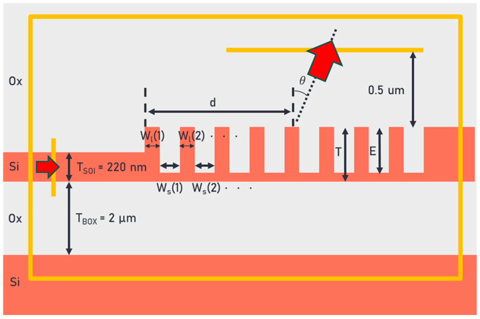
Before designing a fin grating coupler, some constraints must be set to define the geometric structures. The fin gratings can be broken down geometrically into two parts, i.e., indentations or spaces, whose width is represented by
Ws(
n), and protrusions or lines, whose width is represented by
Wl(
n), where a full grating period is represented by
P(
n), which is equal to the summation of the line width and space width. As a result, there are two possible configurations for fin gratings: (1) the SOI waveguide is connected to a line or (2) the SOI waveguide is connected to a space. Here, we choose to connect the SOI waveguide to a line rather than to a space for ease of fabrication, i.e., if the SOI waveguide is connected to a space rather than to a line, the sidewall of the first space is inevitably unable to be smooth and continuous due to the characteristics of ion beam etching, even under ideal conditions in which no lithography errors occur. In
Figure 1, the chosen geometric structures, along with the parameters to be optimized, are illustrated.
Once the geometric structures are chosen, further constraints should be set to optimize the lines, spaces, and periods that maximize the coupling efficiency. The first constraint is that the width of the line Wl(n) should increase as a function of grating index n, because as the light travels from the SOI waveguide through the gratings, it goes from a line of effectively zero in width to, eventually, a line of a constant width. The second constraint is that the width of the space Ws(n) should decrease as a function of grating index n, because as the light travels from the SOI waveguide through the gratings it goes from a space of effectively infinite width to, eventually, a space of a constant width. The increase in the width of the lines and the decrease in the width of the space allows for a smooth transition from the SOI waveguide region to the grating coupler region, acting effectively like a taper. Finally, since the size of the period P(n) is determined by adding up the corresponding line width and the corresponding space width, it can either increase or decrease. However, because of the first and the second constraints considered above, the effective index at the beginning of the gratings is smaller than the effective index at the end of the gratings, which means that the wavenumber of the optical mode increases as the light travels from the beginning of the gratings towards the end of the gratings. This increasing optical mode wavenumber results in multiple emission angles in the direction of light propagation, and to diffract the light into the SMF at the same emission angle, the size of the period should be constrained to decrease as a function of grating index n. Now the trends of Wl(n), Ws(n), and P(n) have been determined, additional constraints due to the fabrication processes should be included. A design rule of >30 nm (DR-30) is chosen when considering the CD of EB lithography, and design rule of >100 nm (DR-100) is chosen when considering the CD of DUV lithography.
In the following, parameters including the width of the line Wl(n), the size of the period P(n), the etch depth E, and the thickness of the grating coupler region T, are optimized given the four constraints on Wl(n), Ws(n), and P(n) discussed above. The SOI thickness is set to a constant of 220 nm and the BOX thickness is set to 2 µm. There are a total of 40 line and space pairs within the grating coupler region, which is 14 µm wide in the direction perpendicular to the light propagation. Note that no bottom reflector is used in conjunction with the grating coupler region.
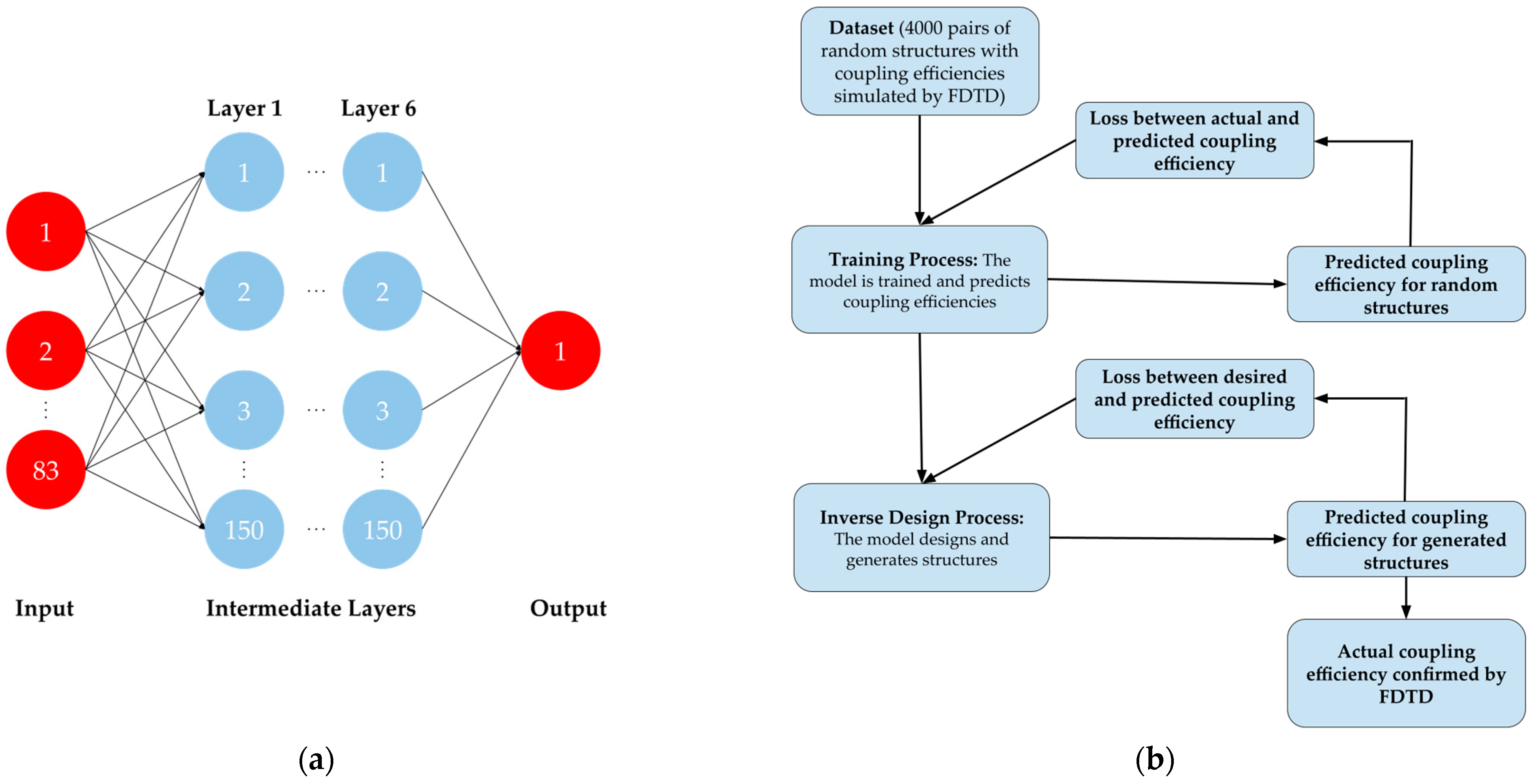
In
Figure 2a, the neural network used in the deep-learning model is shown. It has 83 input parameters (41 line widths; 40 space widths; 1 etch depth; 1 grating coupler region thickness), 1 output result (coupling efficiency), and 6 intermediate layers with 150 nodes per layer, all fully connected to each other. In
Figure 2b, the step-by-step procedure used in the inverse design process is shown. As the first step, a dataset composed of random grating couplers is generated, with information on their respective structural parameters as well as the corresponding coupling efficiencies, simulated by 2D FDTD simulations. A single-mode source for the SOI waveguide is placed at the input of the SOI waveguide and a mode monitor is placed above the grating coupler to calculate the output electric field. We monitor the upward electric field and calculate the overlap integral with the TE mode profile of the SMF-28 fiber, with a core diameter of 8.2 μm. Additionally, monitors are placed at the input of the SOI waveguide and under the grating coupler to calculate the back-reflection and directionality, respectively. The dataset is then fed to the neural network, so that the model is trained with the simulated coupling efficiency and can try to predict the coupling efficiency. The nonlinear activation is carried out by the ReLU function, and the loss function is set to be the mean square error between the actual coupling efficiency (i.e., numbers simulated by FDTD) and the predicted coupling efficiency (i.e., numbers produced by forward inference). The dataset is split so that 70% of the data are for training while the other 30% are for testing. Eventually, after sufficient epochs have passed and a steady state is reached, the accuracy of the model will begin to match the actual accuracy of the FDTD simulations. In the second step, the grating coupler in the dataset that has the highest coupling efficiency is fed to the neural network. Now, by setting the loss function to be the mean-square error between the target coupling efficiency and the predicted coupling efficiency, through backpropagation, without correcting the weights, the structure of the fed grating coupler is adjusted to a higher coupling efficiency according to the gradient map established in the first step. After sufficient iterations have passed and the predicted coupling efficiency has been saturated, the optimal solution for this dataset is found, and FDTD simulations are then performed to confirm its actual coupling efficiency. This two-step process can be repeated several times while decreasing the domain of the input parameters to fully optimize the structure and maximize the coupling efficiency. In the following, three repeats are carried out and the corresponding datasets are referred as datasets 1, 2, and 3.
3. Results and Discussion
The deep-learning model, combined with the proposed inverse design shown in
Figure 2, can achieve a maximum of 80.5% (−0.94 dB) coupling efficiency with the DR-30 constraint and a maximum of 77.9% (−1.09 dB) coupling efficiency with the DR-100 constraint. The coupling efficiency of 80.5% with the e-beam lithography assumption surpasses all previous results for the grating coupler over a single-mode SOI waveguide. On the other hand, the coupling efficiency of 77.9% achieved with the DUV lithography assumption closely matches the previous paper [
17], indicating that the possible maximum efficiency for any grating coupler on 220 nm SOI with DR-100 constraint would likely be around 78%. The clear difference in efficiency between the design rules suggests that the type of fabrication method that is used plays a heavy role in the coupling efficiency of the grating coupler.
In
Table 2, two optimized grating couplers, DR-30 design and DR-100 design, are shown. Four input parameters, including
Wl(
n),
Ws(
n),
E, and
T, as well as six performance metrics, including 1–Backward (i.e., the transmissivity from the SOI waveguide region to the grating coupler region), Directionality (i.e., the power goes upward, divided by the sum of the upward power and downward power), Overlap (i.e., the overlap integral between the optical field 0.5 µm above the grating coupler region and the optical field of the SMF), Angle/Position (i.e., the angle and position of the SMF, optimally chosen corresponding to each design), and Efficiency (i.e., the coupling efficiency), are listed. Note that Efficiency is equal to 1–Backward times Directionality times Overlap. Among the input parameters, the widths of the first lines for the DR-30 and DR-100 designs are 30 nm and 100 nm, respectively, reaching their allowable lower limits. The 668 nm width of the first space for the DR-30 design is larger than the 524 nm width of the first space for the DR-100 design, indicating that the taper is made smoother for the DR-30 design compared to the DR-100 design. In terms of the etch depth and the thickness of the grating coupler region, both DR-30 and DR-100 designs show similar results. Among the performance metrics, there is a large difference between DR-30 and DR-100 designs over the Angle and Position of SMF, which can be explained by the smaller/larger grating wavenumbers (i.e., larger/smaller period sizes) caused by the longer/shorter lengths of the DR-30/DR100 tapers, as well as the weaker/stronger light scatterings caused by the smaller/larger line widths of the DR-30/DR-100 tapers, respectively. Since the DR-100 taper tends to have a larger grating wavenumber at the beginning of the gratings compared to the DR-30 taper, this means the SMF must be tilted at an angle closer to surface normal to better capture the light. Since the DR-100 taper tends to have a stronger scattering at the beginning of the gratings compared to the DR-30 taper, this means the SMF must be located at a position closer to the beginning of the gratings to better capture the light. As for Overlap and Directionality, while both values are high, there seems to be a tradeoff between them. This can be explained by the DR-30 design having a worse directionality (due to weaker light scattering) but a better overlap (due to the smoother, longer taper), while the DR-100 design has a better directionality (due to stronger light scattering) but a worse overlap (due to the less smooth, shorter taper). As for 1–Backward, it can be observed that the DR-30 design has a slightly higher value due to the smoother taper. Finally, for Efficiency, it can be observed that the DR-30 design has a slightly higher value, originating from the better Overlap and 1–Backward, again due to due to the smoother taper.
In
Figure 3, the histograms of the six performance metrics of the DR-30 and DR-100 grating couplers prepared in dataset 1 are plotted. Special attention should be paid to
Figure 3d, in which the best coupling efficiencies in dataset 1 do not exceed 80% for both DR-30 and DR-100 designs. Note that, rather than using these random grating couplers to immediately improve the coupling efficiency, the aim was to establish a high-dimensional gradient map that could be used to further improve coupling efficiency down the line. To further correlate the four input parameters and the six performance metrics,
Figure 4 is plotted and configured so that the horizontal axis represents the four input parameters, the vertical axis represents the five performance metrics 1-Backward, Directionality, Overlap, Angle, and Position, and the color axis represents the performance metric Efficiency, only for the DR-30 grating couplers prepared in dataset 1. From there, it can be observed that some of the input parameters heavily affect some of the performance metrics and eventually influence the coupling efficiency. For example, most of the grating couplers with the best efficiencies tend to cluster in the region where (1) the width of the first space is between 550 nm and 750 nm and (2) the etch depth to the thickness of the grating coupler region is around 0.6. Moreover, there is a clear trade-off between Directionality and Overlap as a function of the thickness of the grating coupler region, which has been explained in the previous paragraph through the strength of the light scattering, as well as the smoothness and length of the taper.
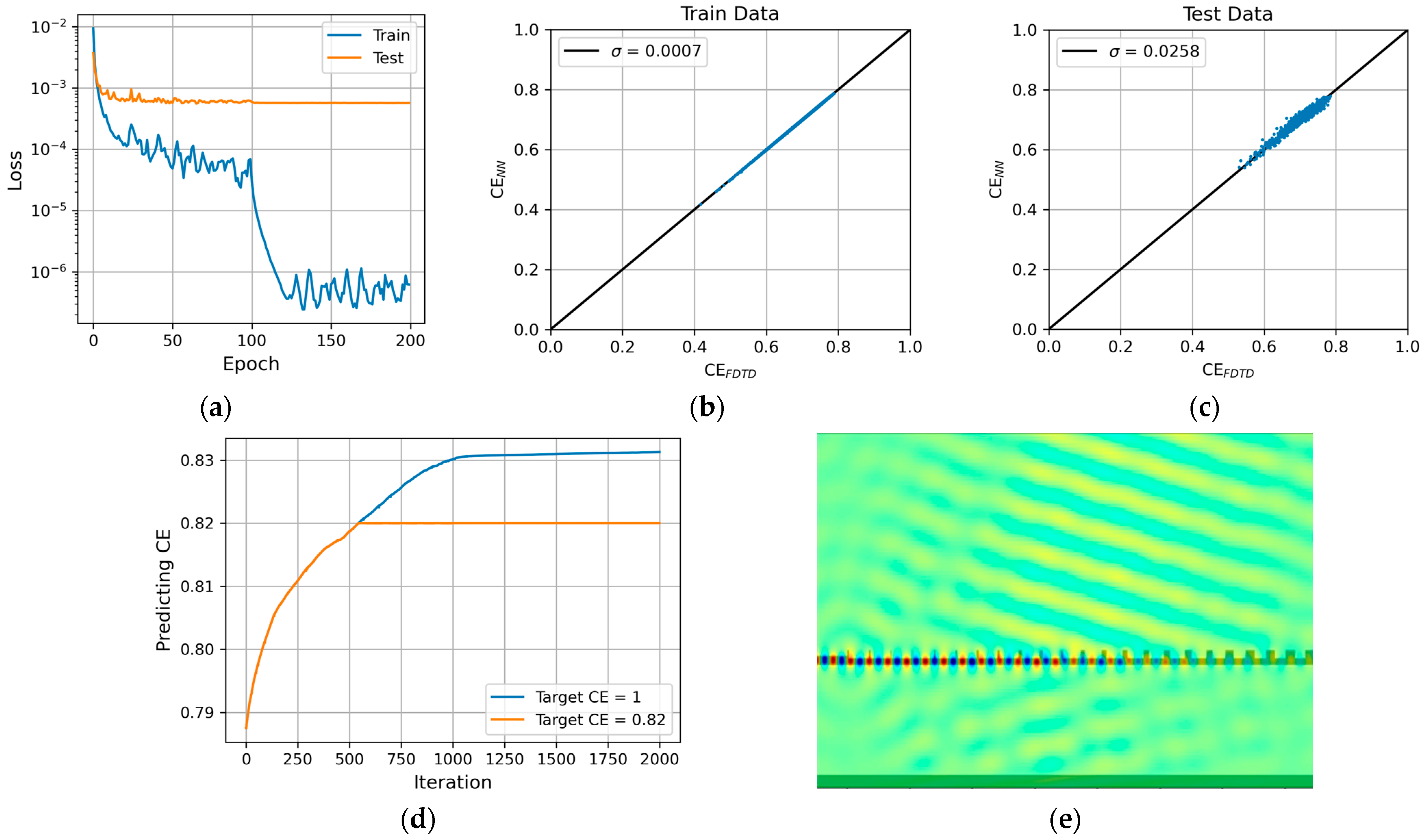
In
Figure 5, the data relevant to the training process and inverse design process for the DR-30 grating couplers prepared in dataset 3 are plotted. During the training process, it takes about 200 epochs for the train dataset to saturate around 10
−6, while for the test dataset it only takes about 100 epochs to saturate around 10
−3 (see
Figure 5a). To ensure the accuracy of the model, comparisons between the actual coupling efficiency (i.e., that simulated by FDTD) and the predicted coupling efficiency (i.e., that predicted by the neural network) are made. For both the training and test datasets, the correlations between the actual and the predicted coupling efficiency are very good, with an error of about 0.07% and 2.58% for the training and test dataset, respectively (see
Figure 5b,c). During the inverse design process, the maximally predicted coupling efficiency when 1 is assigned as the target coupling efficiency saturates at 83.1% (see
Figure 5d) after approximately 1000 interactions with the initial structure (i.e., the best DR-30 grating coupler in dataset 3), which is then verified by FDTD as only 80.2%. We also examine the cases with a lower target coupling efficiency and find that when 0.82 is assigned as the target coupling efficiency, the maximally predicted coupling efficiency saturates at 82% (see
Figure 5d) after approximately 500 iterations of the initial structure, and is then verified by FDTD as 80.5%, which is the highest value we can obtain with different target coupling efficiencies. The electrical field profile and the structure of the final optimal grating coupler are shown in
Figure 5e. Note that we also calculate the (spectral) bandwidth and the back-reflection of the final optimal grating coupler. The demonstrated 3-dB bandwidth and back-reflection are both very promising and can reach as high as 73 nm and as low as −20.9 dB, respectively.
4. Deep Learning and Covariance Matrix Adaptation Evolution Strategy
To verify that a globally maximum coupling efficiency is reached by the studied deep-learning model and inverse design process, we apply a conventional optimization approach CMA-ES [
11] to benchmark our results. CMA-ES is an evolutional strategy that attempts to mimic the natural adaptation process, involving the generation of many candidate structures that evolve over successive generations. CMA-ES is distinct from other evolutional strategies because it uses a covariance matrix to model the relationships between different parameters, which allows for a better modeling of non-linear relationships. The implementation of the CMA-ES starts with a multivariate normal distribution. Structures are then sampled from this distribution and, after being evaluated by an FDTD simulator, different structures are then sorted according to the evaluated coupling efficiency, in which the best structures from the batch are taken to create a new distribution. New structures are then sampled from this updated distribution. This whole cycle will repeat itself until the evaluated coupling efficiency saturates. Through this cyclical process, we can achieve a new high accuracy of 82.7% for DR-30 design and 78.9% for DR-100 design. Further comparisons between the structural parameters, as shown in
Figure 6, specifically the widths of the lines and spaces as a function of the grating index, are made for the gradient method (i.e., the studied deep-learning model combined with the inverse design process, because this is essentially a gradient method in which the gradient map is obtained during the training process) and CMA-ES. It can be observed that the structural parameters of the two approaches closely match each other, suggesting that a globally maximum coupling efficiency has been reached by the gradient method, and further improvements in coupling efficiency using any other optimization algorithms will likely result in minor improvements. Finally, we apply one-tenth of the process limit as the fabrication errors, where, for DUV and e-beam, they correspond to 10 nm and 3 nm, respectively. Under these conditions, we simulate the changes in fin width caused by the fabrication errors, resulting in efficiency reductions of 0.04 dB given ±10 nm variation and 0.01 dB given ±3 nm variation for DUV and e-beam, respectively. This demonstrates the remarkably stable performance of the final optimal grating couplers.
5. Conclusions
In conclusion, we propose a procedure that utilizes the neural network to conduct an inverse design of the grating coupler that satisfies the conditions of single-mode operation (SOI thickness = 220 nm < 245 nm), a simple fabrication process, and no bottom mirror. We also propose physical constraints that generate quality data for training the neural network, instead of generating the fully random data that are commonly used in the literature. This mitigates the drawback of huge amounts of data being required for neural network training, and therefore significantly improves the training efficiency. By utilizing a deep-learning model in conjunction with an inverse design process, we construct an efficient grating coupler with a coupling loss < 1 dB, which is, to our knowledge, the lowest coupling loss for grating couplers over a single-mode SOI waveguide. The relations between the input parameters and the performance metrics are studied in detail to provide insights into the trade-offs within the design. We then verify the structure of the designed grating coupler using a conventional optimization approach, CMA-ES, showing that the solution obtained by the deep-learning-based inverse design is indeed globally optimized. Note that we prepare three datasets for training the neural network, with each dataset containing 4000 sets of data. The CMA-ES method requires 600 iterations, with each iteration consisting of 20 sets of data. Therefore, the total amount of simulation data is the same for both methods. While the neural network requires additional time for training, this is negligible compared to the time needed for FDTD simulations.


