3. Results and Discussions
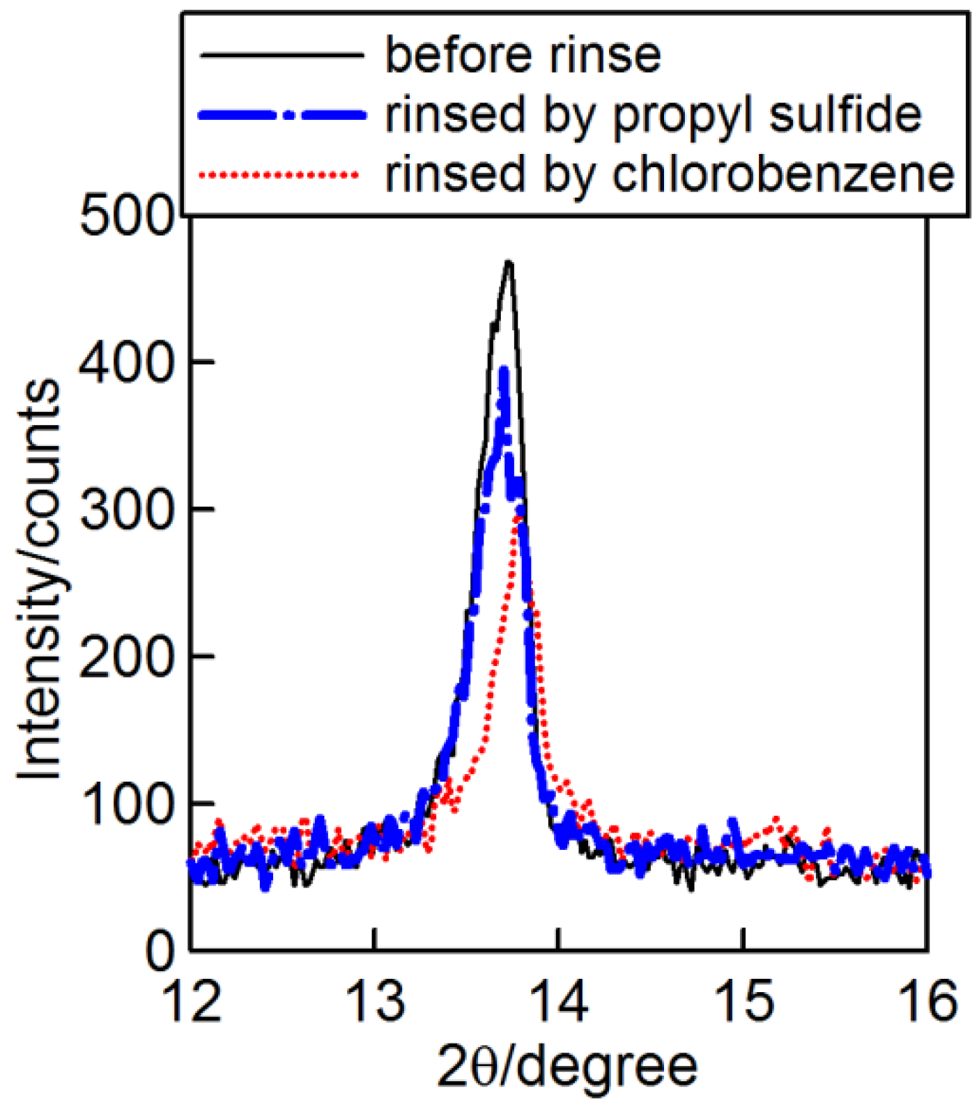
At first, the solvent-rinsing effect on CH
3NH
3PbI
3 perovskite crystal variation was considered before the HTM deposition itself.
Figure 1 shows the XRD patterns of the CH
3NH
3PbI
3 perovskite crystal after spin-coating chlorobenzene (solvent of spiro-OMeTAD) and propyl sulfide (solvent of CuSCN) on one-step processed CH
3NH
3PbI
3 perovskite layers. The original CH
3NH
3PbI
3 perovskite crystal showed the XRD peak at 13.7° and 468 counts. Although the intensity of XRD counts was related to the measurement setup, the height between the samples can be compared to discuss the variation of crystal structures using the same system consistently. It was surprising that just spin-coating chlorobenzene, which has been used for the spiro-OMeTAD deposition as an inert solvent against the CH
3NH
3PbI
3 perovskite crystal, can shift the peak to a higher angle and reduce the height of the XRD peak to half of the original one. The XRD peak shift to a higher angle means that the crystal lattice became shorter. This phenomenon may be due to the extraction of remaining DMF in the perovskite layer to chlorobenzene, which was explained as the “antisolvent method” published by Xiao
et al. [
14]. This result informs us that the remaining DMF in the perovskite crystal after the annealing procedure can be removed, because of the softness of the CH
3NH
3PbI
3 perovskite crystal [
6,
7]. In contrast, propyl sulfide (the solvent of CuSCN) did not change the XRD peak of the CH
3NH
3PbI
3 perovskite crystal, but reduced the XRD peak height. Since solvents (chlorobenzene and propyl sulfide) reduce the XRD peak of the CH
3NH
3PbI
3 perovskite crystal, the deposition of HTM by spin-coating can reduce the crystallinity of CH
3NH
3PbI
3 perovskite due to the solvent effect.
Figure 1.
XRD patterns of one-step-processed CH3NH3PbI3 perovskite layers varied by solvent rinsing on the perovskite layer.
Figure 1.
XRD patterns of one-step-processed CH3NH3PbI3 perovskite layers varied by solvent rinsing on the perovskite layer.
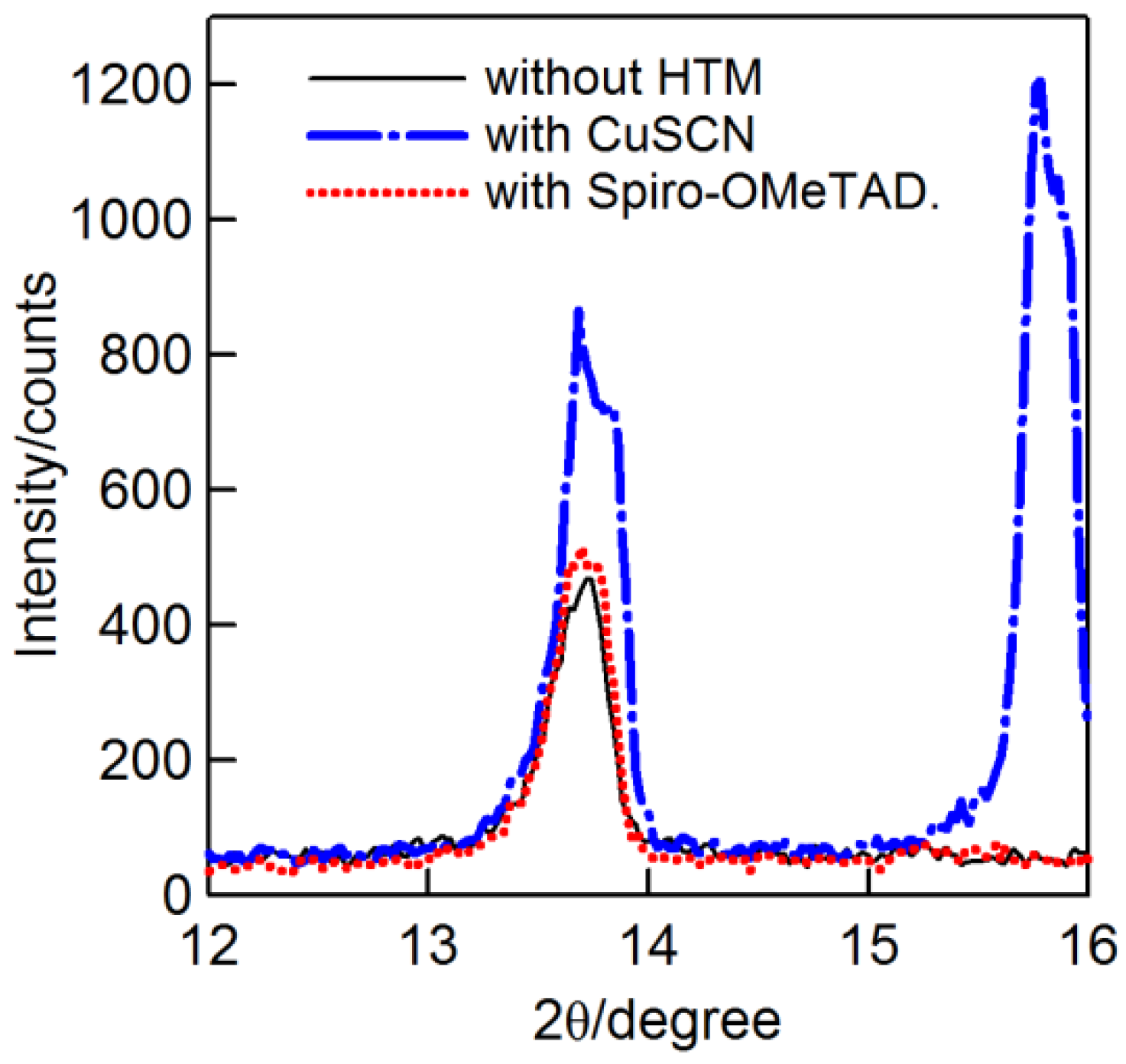
Figure 2 shows the XRD patterns of one-step-processed CH
3NH
3PbI
3 perovskite crystals with HTM layers. The peak at 15.8° represents the crystal of the CuSCN layer. It was surprising that CuSCN deposition enhanced the crystallinity of CH
3NH
3PbI
3 perovskite, which may be due to the Cu
+-ion and SCN
−-ion migration into CH
3NH
3PbI
3 perovskite, resulting in the enhancement of the perovskite crystal. Actually, CH
3NH
3Pb(SCN)
2I can also be a perovskite solar cell, effectively [
15]. In contrast, the XRD pattern of CH
3NH
3PbI
3 perovskite did not change with spiro-OMeTAD deposition. Hence, it was considered that the solvent of spiro-OMeTAD (chlorobenzene) can shift the XRD peak position to the higher angle, but that the dopant (which may be lithium ion and TBP) can shift it back to the original position, due to the special phenomena of material migration in the CH
3NH
3PbI
3 perovskite crystal [
6,
7].
Figure 2.
XRD patterns of one-step-processed CH3NH3PbI3 perovskite layers varied by hole-conducting materials (HTM) on the perovskite layer. 2,2’,7,7’-Tetrakis-(N,N-di-p-methoxyphenylamine)-9,9’-spirobifluorene is represented as “spiro-OMeTAD”.
Figure 2.
XRD patterns of one-step-processed CH3NH3PbI3 perovskite layers varied by hole-conducting materials (HTM) on the perovskite layer. 2,2’,7,7’-Tetrakis-(N,N-di-p-methoxyphenylamine)-9,9’-spirobifluorene is represented as “spiro-OMeTAD”.
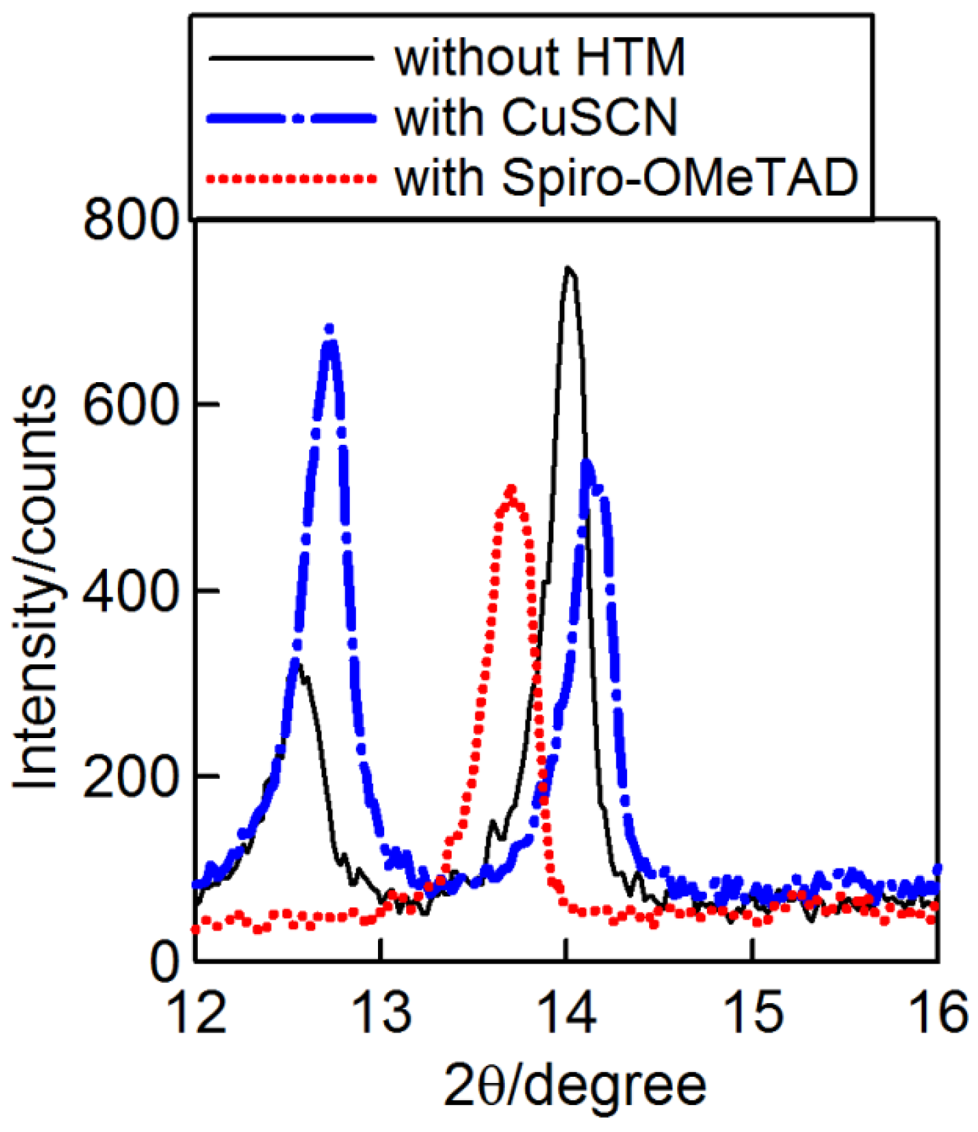
Figure 3 shows the XRD patterns of the two-step deposition of the CH
3NH
3PbI
3 perovskite crystal with the HTM layer. Due to the procedure of the two-step sequential deposition of the PbI
2 crystal into methylammonium iodide solution, some part of the PbI
2 can remain [
9]. Although the CuSCN XRD peak can remain on the one-step deposited CH
3NH
3PbI
3 (15.8°, in
Figure 2), it was found that the peak of CuSCN vanished on the two-step-deposited CH
3NH
3PbI
3 perovskite layer, which may be due to the attack of the excess amount of iodide ion from the PbI
2 layer on the CuSCN crystal. It was also proposed that the thiocyanate ion (SCN
−) can migrate to the PbI
2 layer and can be exchanged with the ion with iodide ion (I
−) to form the CH
3NH
3Pb(SCN)
2I perovskite crystal, resulting in the emission of the iodide ion to the CuSCN layer to be some amorphous phase. Hence, we can observe the shift of the PbI
2 layer. Moreover, the CuSCN can shift the XRD pattern of CH
3NH
3PbI
3 perovskite to a higher angle and lower intensity. Therefore, CuSCN can be mixed with the CH
3NH
3PbI
3 perovskite crystal effectively. In contrast, the effect of spiro-OMeTAD coating on the two-step-processed perovskite is also quite significant, because the spiro-OMeTAD coating causes the peak of PbI
2 to vanish and can shift the perovskite peak to the same position with the one-step-deposited CH
3NH
3PbI
3 perovskite. This PbI
2 decomposition may be due to the attack of the lithium ion and TBP on the PbI
2 crystal.
It was confirmed that the CH3NH3PbI3 perovskite crystal was quite soft, and it was easy to change the lattice with the deposition of the HTM layer. In order to stabilize the CH3NH3PbI3 perovskite crystal, we have attempted doping with other halogens (chloride and bromide) and 5-aminovaleric acid (AVA) in the CH3NH3PbI3 perovskite crystal.
Figure 3.
XRD patterns of the two-step-processed CH3NH3PbI3 perovskite layers varied by hole-conducting materials (HTM) on the perovskite layer. 2,2’,7,7’-Tetrakis-(N,N-di-p-methoxyphenylamine)-9,9’-spirobifluorene is represented as “spiro-OMeTAD”.
Figure 3.
XRD patterns of the two-step-processed CH3NH3PbI3 perovskite layers varied by hole-conducting materials (HTM) on the perovskite layer. 2,2’,7,7’-Tetrakis-(N,N-di-p-methoxyphenylamine)-9,9’-spirobifluorene is represented as “spiro-OMeTAD”.
Figure 4 shows the doping effects of Cl
− and Br
− ions on the CH
3NH
3PbI
3 perovskite and HTM layers. Although there are some publication about Cl
− and Br
− ions, which can enhance the crystallinity and stability of the CH
3NH
3PbI
3 perovskite crystal [
10,
11],
Figure 4 suggests that Cl
− and Br
− ions cannot stabilize the CH
3NH
3PbI
3 crystal against HTM deposition. It was confirmed that the doping of Cl
− and Br
− ions can greatly reduce or cause the XRD peak of CuSCN to vanish, which should arise around 15.8° (as in
Figure 2). Actually, the chloride ion can improve the crystallinity of CH
3NH
3PbI
3 perovskite with over 10,000 counts of XRD (
Figure 4a). However, the HTM deposition of spiro-OMeTAD or CuSCN can reduce the XRD intensity and shift the position of the XRD peak. Specially, the deposition of spiro-OMeTAD can reduce the XRD peak of the CH
3NH
3PbI
3 perovskite crystal very significantly. With the bromide ion, the XRD peak of CH
3NH
3PbI
3 perovskite can improve with the incorporation of CuSCN (
Figure 4b). The vanishing effect of the CuSCN peak by the chloride ion is stronger than that by the bromide ion.
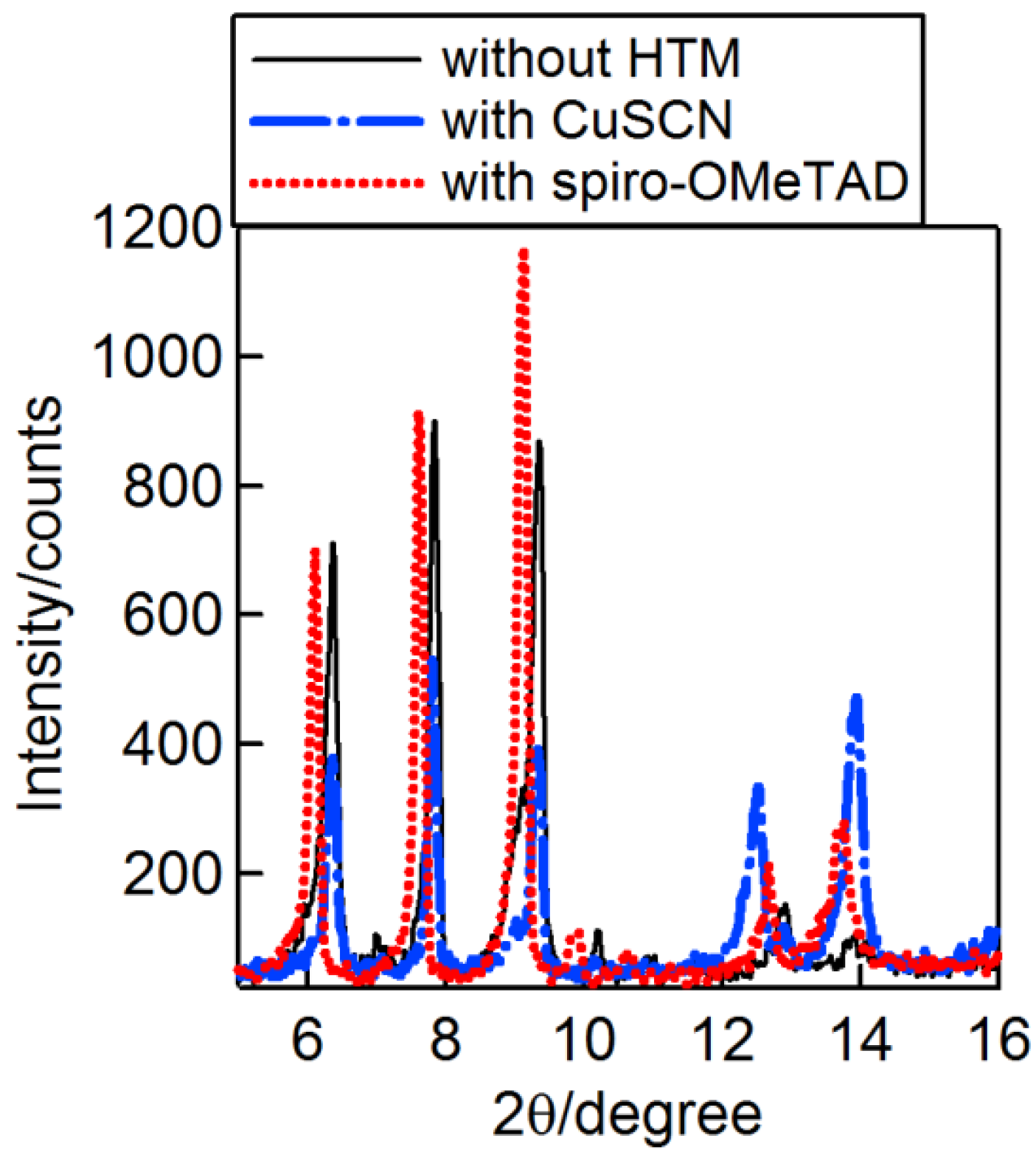
Figure 5 shows the XRD patterns of the 5-AVA-doped CH
3NH
3PbI
3 perovskite crystal by spin-coating deposition. Although only one XRD peak of 5-AVA-doped CH
3NH
3PbI
3 perovskite was observed below 10° in the literature [
12], three intense peaks from 6° to 10° were observed as the 2D CH
3NH
3PbI
3 perovskite crystal. The difference from the published results may be due to the fabrication methods: spin-coating and drop casting. Without HTM, the peaks of the three-dimensional (3D) CH
3NH
3PbI
3 perovskite crystal (at 13.9°) and PbI
2 (at 12.9°) were quite small. Adding CuSCN HTM, the peak position of the 2D CH
3NH
3PbI
3 perovskite crystal did not change, but the peak height was decreased to less than half. At the same time, the peaks of the 3D CH
3NH
3PbI
3 perovskite crystal (at 13.9°) and PbI
2 (at 12.5°) were increased significantly. The peak height of the 3D CH
3NH
3PbI
3 perovskite crystal became very close to the one-step-processed CH
3NH
3PbI
3 perovskite. Adding spiro-OMeTAD, in contrast, the peak position of the 2D CH
3NH
3PbI
3 perovskite crystal was shifted to the lower angle, and the peak height was increased. Although the peaks of the 3D CH
3NH
3PbI
3 perovskite crystal and PbI
2 were increased, the increment by spiro-OMeTAD was half of that by CuSCN. Hence, spiro-OMeTAD did not change the 2D CH
3NH
3PbI
3 perovskite crystal, but some of the contents (maybe the lithium ion and TBP) can be inserted between the 2D CH
3NH
3PbI
3 perovskite layers, which can be explained by the peak shift of 2D perovskite to the lower angle. Such a 2D perovskite layer has stability against moisture [
12,
16]. However, it was confirmed that such a 2D perovskite also can be changed by HTM deposition.
Figure 4.
XRD patterns of one-step-processed CH3NH3PbI3 perovskite layers with chloride and/or bromide doping, varied by hole-conducting materials (HTM) on the perovskite layer with chloride doping (a) and with bromide doping (b). 2,2’,7,7’-Tetrakis-(N,N-di-p-methoxyphenylamine)-9,9’-spirobifluorene is represented as “spiro-OMeTAD”.
Figure 5.
XRD patterns of the one-step-processed CH3NH3PbI3 perovskite layers with 5-aminovaleric acid (5-AVA) doping, varied by hole-conducting materials (HTM) on the perovskite layer. 2,2’,7,7’-Tetrakis-(N,N-di-p-methoxyphenylamine)-9,9’-spirobifluorene is represented as “spiro-OMeTAD”.
Figure 5.
XRD patterns of the one-step-processed CH3NH3PbI3 perovskite layers with 5-aminovaleric acid (5-AVA) doping, varied by hole-conducting materials (HTM) on the perovskite layer. 2,2’,7,7’-Tetrakis-(N,N-di-p-methoxyphenylamine)-9,9’-spirobifluorene is represented as “spiro-OMeTAD”.
However, it was found that the resulting PbI
2 layer from the 2D CH
3NH
3PbI
3 perovskite layer has higher stability than the 3D perovskite crystal.
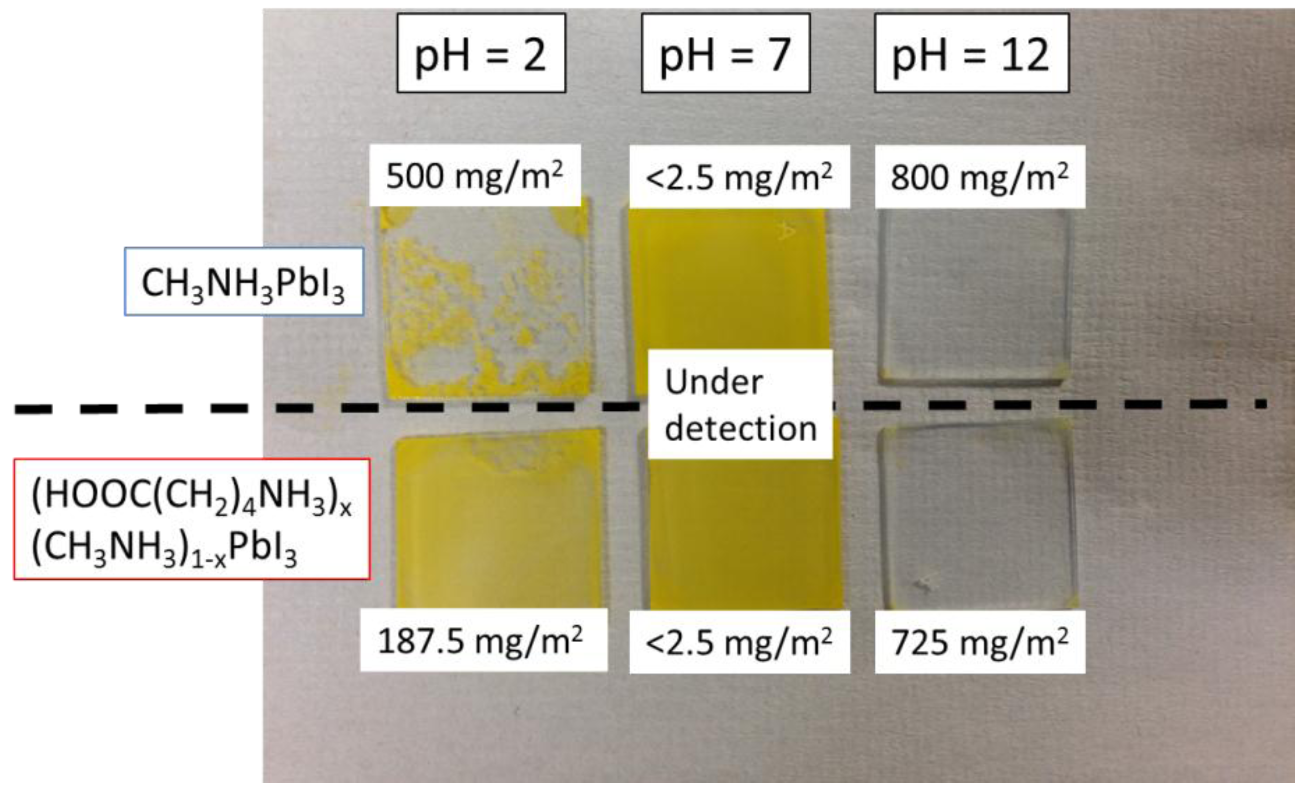
Figure 6 shows a picture of PbI
2 layers after water deposition (with different pH) of CH
3NH
3PbI
3 perovskite layers (with/without 5-AVA doping). The CH
3NH
3PbI
3 perovskite layers with/without 5-AVA doping have been decomposed to PbI
2 by dipping in water. When the amount of eluted Pb in the water was measured, no elution of Pb was observed using neutral water (pH = 7). However, alkaline water solution (pH = 12 of NaOH aq. solution) dissolved the CH
3NH
3PbI
3 perovskite layers completely. The observed amounts of Pb ion using CH
3NH
3PbI
3 perovskite layers with/without 5-AVA doping were 800 mg/m
2 and 725 mg/m
2, respectively. This small variation may be due to the difference of thickness after the 5-AVA doping. The significant difference of doping was confirmed using acidic water solution (pH = 2, HCl aq. solution). The 5-AVA doping can enhance the stability of the PbI
2 crystal against acidic water solution. This kind of effort to suppress the leakage of Pb elution should be improved for the application of organo lead halide perovskite solar cells.
Figure 6.
Pictures of the one-step-processed CH3NH3PbI3 perovskite layers with/without 5-aminovaleric acid (5AVA) doping, dipped in water, aqueous HCl solution (pH = 2) and aqueous NaOH solution (pH = 12). The numbers inserted in the picture show the amount of the lead dissolved into the water, the aqueous HCl solution (pH = 2) and the aqueous NaOH solution (pH = 12).
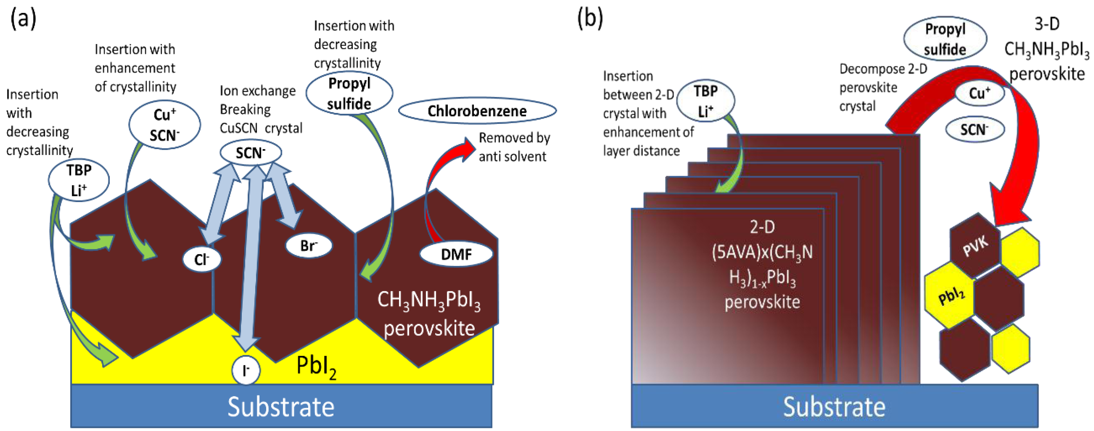
Figure 7 shows a summary of the reaction image between the CH
3NH
3PbI
3 perovskite crystal for the deposition of solvents (chlorobenzene and propyl sulfide) and HTM (spiro-OMeTAD and CuSCN). Chlorobenzene can extract DMF in the non-dried perovskite layer [
14]. Moreover, the chlorobenzene may have a similar effect on the annealed perovskite layer (from
Figure 1). In contrast, propyl sulfide did not shift the peak position, but decreased the intensity due to the decomposing of the smaller crystal (from
Figure 1). The thiocyanate ion (SCN
−) can be exchanged by the iodide ion (I
−) in PbI
2 [
15] and by the chloride (Cl
−) and bromide (Br
−) ions doped in perovskite crystals to be CH
3NH
3Pb(SCN)
2I perovskite [
15], resulting in the prevention of the CuSCN crystal on the CH
3NH
3PbI
3 perovskite layer (from
Figure 2,
Figure 3 and
Figure 4). The Cu
+ ion and the SCN
− ion can enhance the crystallinity of CH
3NH
3PbI
3 perovskite. However, the chloride ion and the excess amount of I
− (from PbI
2) can suppress the enhancement of the CH
3NH
3PbI
3 perovskite crystallinity. For the 2D (5-AVA)
x(CH
3NH
3)
1-xPbI
3 perovskite crystal, the lithium ion and TBP in spiro-OMeTAD HTM can be inserted between the layered perovskite crystal (as in
Figure 7b, from
Figure 5). The deposition of CuSCN HTM can convert the 2D crystal to a 3D one.
In order to discuss the CH
3NH
3PbI
3 perovskite crystal transformation, the water content (purity) in the solvents, HTM materials and atmosphere should be explained, because water can decompose the CH
3NH
3PbI
3 perovskite crystal into PbI
2 ([
16]; as in
Figure 6). In this work, the humidity of the laboratory was 60% to 80%. The contents of water in the HTM materials and the solvents were not measured. However, the HTM depositions did not enhance the PbI
2 peak during the experiments, basically (only one exception was the two-step-processed CH
3NH
3PbI
3 perovskite with CuSCN HTM in
Figure 3). Therefore, it is considered that the effect of water can be negligible. For the further study of the stability of perovskite solar cells, the amount of water in HTM would be very important.
Figure 7.
Summary of the reaction scheme of organo lead halide perovskite layers for CH3NH3PbX3 (X: I, Cl or Br) (a) and for (HOOC(CH2)4NH3)x(CH3NH3)1-xPbI3 (b).
Figure 7.
Summary of the reaction scheme of organo lead halide perovskite layers for CH3NH3PbX3 (X: I, Cl or Br) (a) and for (HOOC(CH2)4NH3)x(CH3NH3)1-xPbI3 (b).
Moreover, some molecules (DMF, DMSO,
etc.) were known to be inserted into the crystal lattice, as studied by Yang
et al. [
5]. In this work, the experiments had been performed in laboratory fume hoods. No glovebox was used for the experiments. Hence, it was considered that the effect of volatile solvent on the perovskite surface from air was eliminated effectively. Of course, there is a chance that the changes by solvent exposure are irreversible or returned (recovered) after annealing of the perovskite layer, as reported by Jeon
et al. [
17], which is generally carried out for the completion of a stand-alone perovskite layer. However, the aim of this paper is to show the instability against HTM deposition, which will not be annealed after the HTM deposition. Moreover, Cu
2+, SCN
− and Li
+ are non-volatile ions. Hence, we would like to skip the annealing effect of crystal recovery after HTM deposition for future studies.
The decomposition mechanism of the CH3NH3PbI3 perovskite crystal by the lithium ion and TBP was speculated as the exchanging effect with the methyl ammonium ion (CH3NH3+). Basically, TBP is a strong base, which can exchange H+ with water or CH3NH3+. In contrast, it can be speculated that the lithium ion and TBP can be inserted into the hydrogen bonding (R-COOH···HOOC-R; the dot line “···” represents hydrogen bonding) in the gap between the 5-AVA-ion (HOOC(CH2)4NH3+)-doped 2D perovskite crystals. Further research will be performed to elucidate the exact mechanism.


