Absorption Properties of Simply Fabricated All-Metal Mushroom Plasmonic Metamaterials Incorporating Tube-Shaped Posts for Multi-Color Uncooled Infrared Image Sensor Applications


Abstract
:
1. Introduction
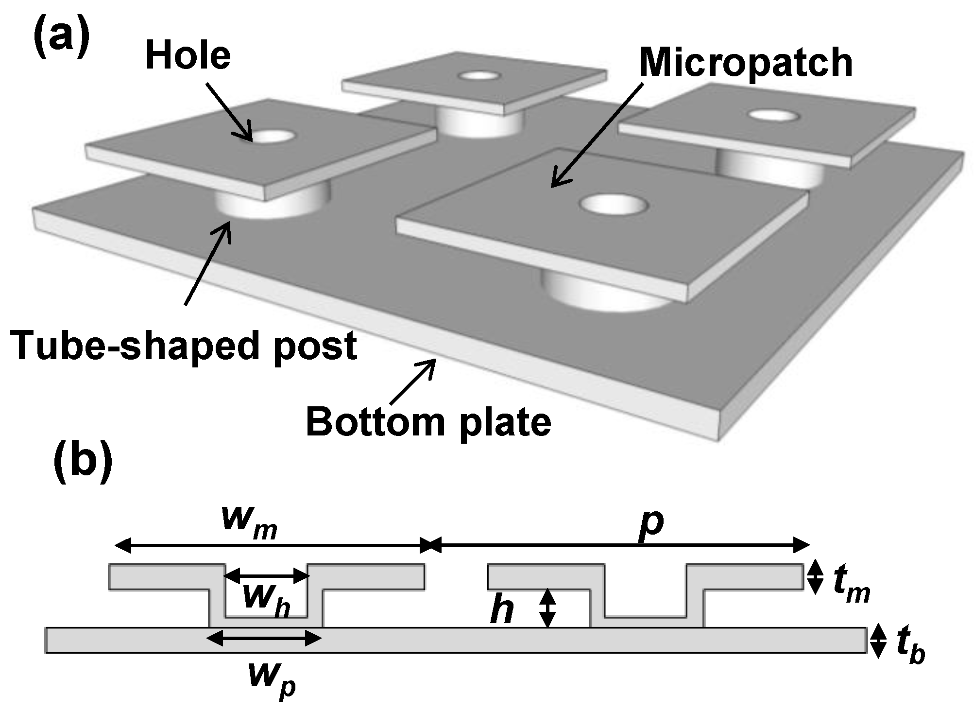
2. Absorber Design
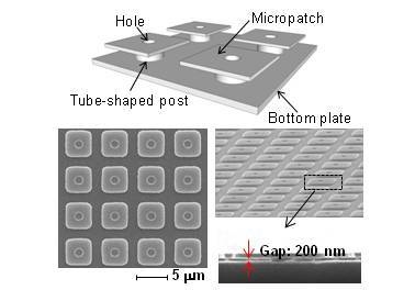
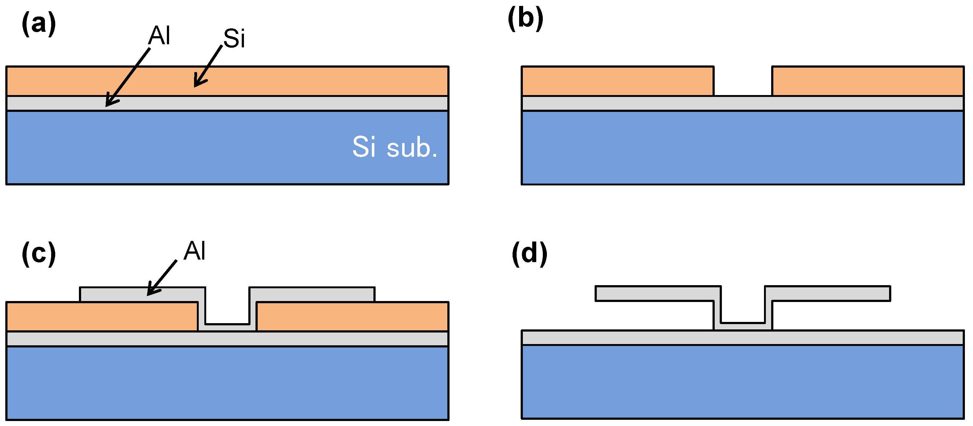
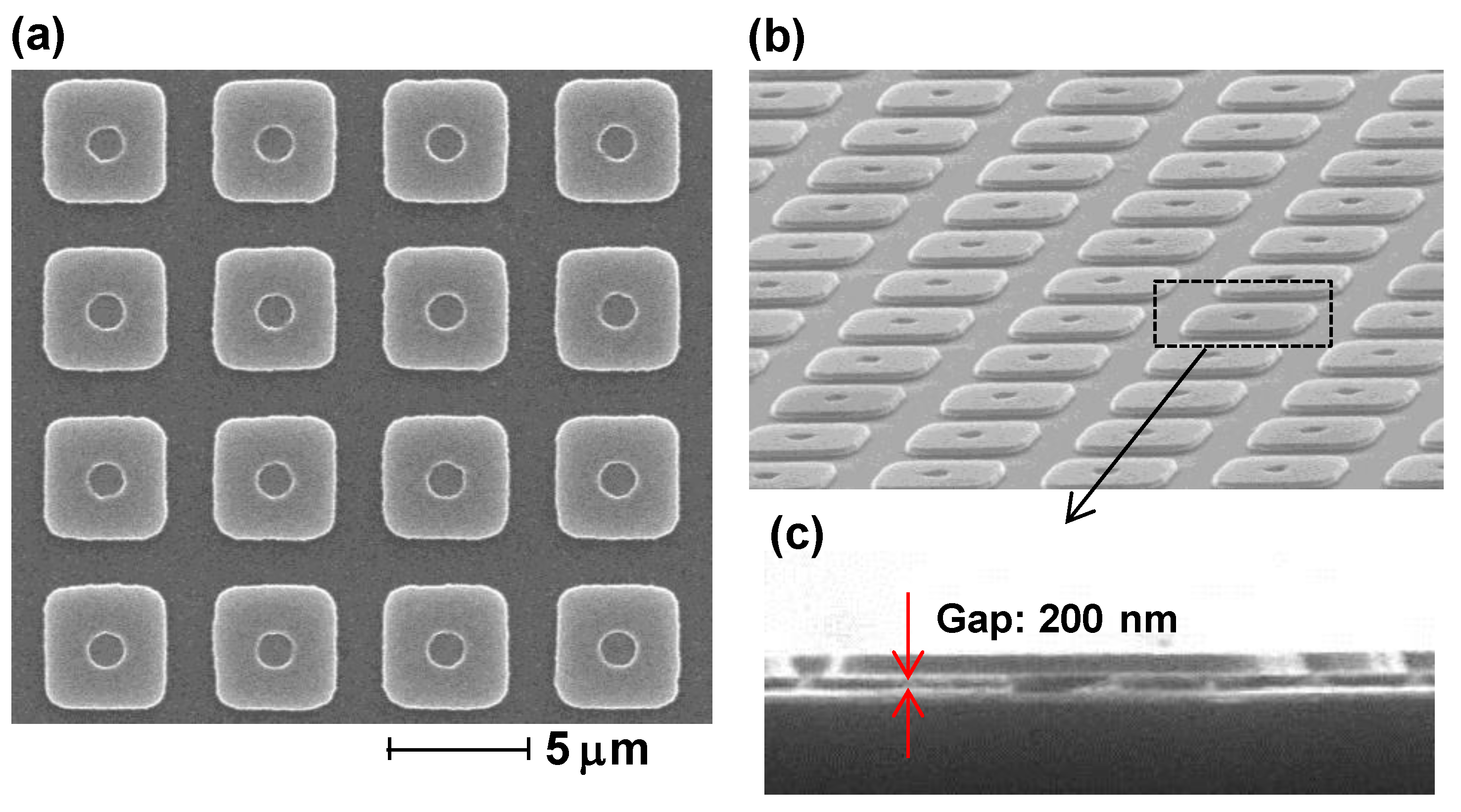
3. Fabrication
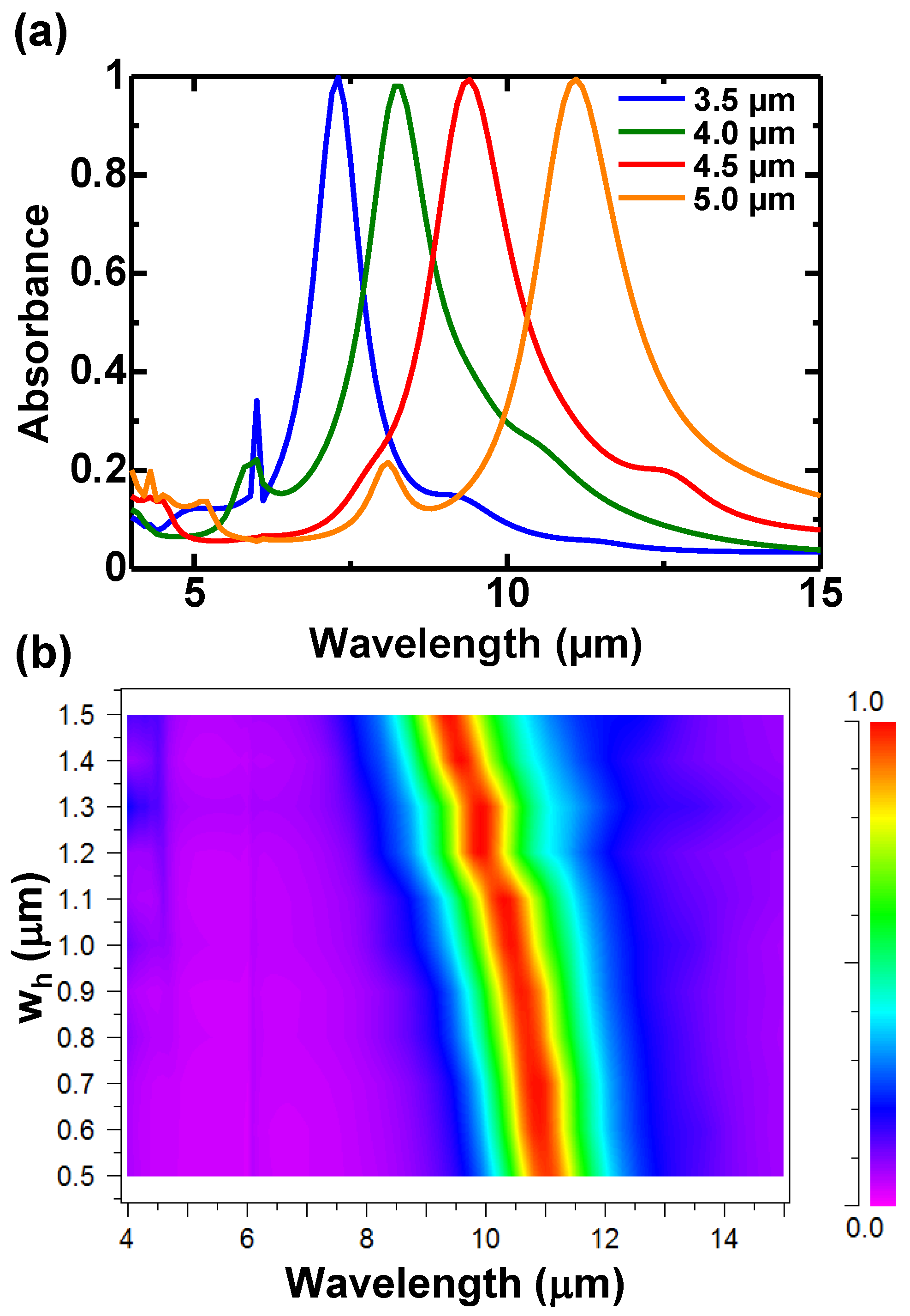
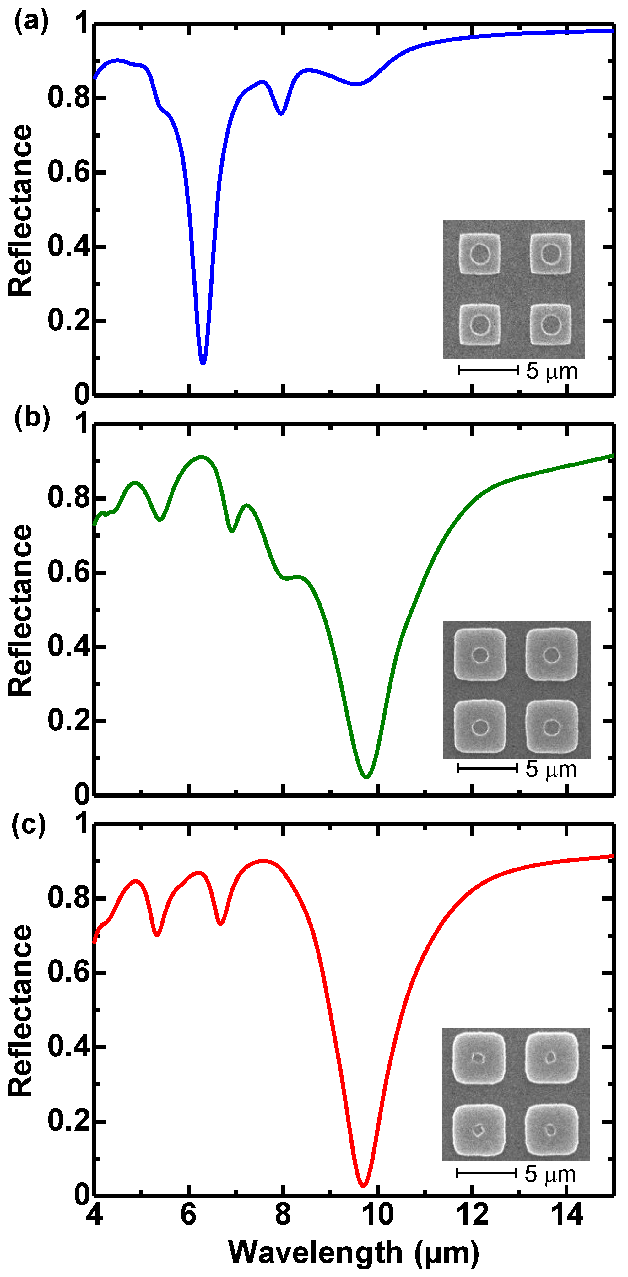
4. Measurement and Discussion
5. Conclusions
Acknowledgments
Author Contributions
Conflicts of Interest
Abbreviations
| IR | Infrared |
| MPMAT | Mushroom plasmonic metamaterial absorber incorporating tube-shaped metal posts |
| LWIR | long-wavelength IR |
| EW | Electromagnetic wave |
| MIM | Metal-insulator-metal |
| CMOS | Complementary metal oxide semiconductor |
| RCWA | Rigorous coupled wave analysis |
| RIE | Reactive ion etching |
| SEM | Scanning electron microscopy |
| FTIR | Fourier transform infrared spectroscopy |
References
- Stanley, R. Plasmonics in the mid-infrared. Nat. Photon. 2012, 6, 409–411. [Google Scholar] [CrossRef]
- Kawata, S. Plasmonics: Future outlook. Jpn. J. Appl. Phys. 2013, 52, 010001. [Google Scholar] [CrossRef]
- Smith, D.R.; Pendry, J.B.; Wiltshire, M.C. Metamaterials and negative refractive index. Science 2004, 305, 788–792. [Google Scholar] [CrossRef] [PubMed]
- Meinzer, N.; Barnes, W.L.; Hooper, I.R. Plasmonic meta-atoms and metasurfaces. Nat. Photon. 2014, 8, 889–898. [Google Scholar] [CrossRef] [Green Version]
- Watts, C.M.; Liu, X.; Padilla, W.J. Metamaterial electromagnetic wave absorbers. Adv. Mater. 2012, 24, OP98–OP120. [Google Scholar] [CrossRef] [PubMed]
- Aydin, K.; Ferry, V.E.; Briggs, R.M.; Atwater, H.A. Broadband polarization-independent resonant light absorption using ultrathin plasmonic super absorbers. Nat. Commun. 2011, 2, 517. [Google Scholar] [CrossRef] [PubMed]
- Liu, N.; Mesch, M.; Weiss, T.; Hentschel, M.; Giessen, H. Infrared perfect absorber and its application as plasmonic sensor. Nano Lett. 2010, 10, 2342–2348. [Google Scholar] [CrossRef] [PubMed]
- Ishikawa, A.; Tanaka, T. Metamaterial absorbers for infrared detection of molecular self-assembled monolayers. Sci. Rep. 2015, 5, 12570. [Google Scholar] [CrossRef] [PubMed] [Green Version]
- Maier, T.; Brueckl, H. Multispectral microbolometers for the midinfrared. Opt. Lett. 2010, 35, 3766–3768. [Google Scholar] [CrossRef] [PubMed]
- Ogawa, S.; Okada, K.; Fukushima, N.; Kimata, M. Wavelength selective uncooled infrared sensor by plasmonics. Appl. Phys. Lett. 2012, 100, 021111. [Google Scholar] [CrossRef]
- Ogawa, S.; Komoda, J.; Masuda, K.; Kimata, M. Wavelength selective wideband uncooled infrared sensor using a two-dimensional plasmonic absorber. Opt. Eng. 2013, 52, 127104. [Google Scholar] [CrossRef]
- Ogawa, S.; Masuda, K.; Takagawa, Y.; Kimata, M. Polarization-selective uncooled infrared sensor with asymmetric two-dimensional plasmonic absorber. Opt. Eng. 2014, 53, 107110. [Google Scholar] [CrossRef]
- Alves, F.; Grbovic, D.; Karunasiri, G. Investigation of microelectromechanical systems bimaterial sensors with metamaterial absorbers for terahertz imaging. Opt. Eng. 2014, 53, 097103. [Google Scholar] [CrossRef]
- Tao, H.; Kadlec, E.A.; Strikwerda, A.C.; Fan, K.; Padilla, W.J.; Averitt, R.D.; Shaner, E.A.; Zhang, X. Microwave and terahertz wave sensing with metamaterials. Opt. Exp. 2011, 19, 21620–21626. [Google Scholar] [CrossRef] [PubMed]
- Ding, F.; Cui, Y.; Ge, X.; Jin, Y.; He, S. Ultra-broadband microwave metamaterial absorber. Appl. Phys. Lett. 2012, 100. [Google Scholar] [CrossRef]
- Wang, B.; Teo, K.H.; Nishino, T.; Yerazunis, W.; Barnwell, J.; Zhang, J. Experiments on wireless power transfer with metamaterials. Appl. Phys. Lett. 2011, 98, 254101. [Google Scholar] [CrossRef]
- Talghader, J.J.; Gawarikar, A.S.; Shea, R.P. Spectral selectivity in infrared thermal detection. Light Sci. Appl. 2012, 1. [Google Scholar] [CrossRef]
- Fujisawa, D.; Ogawa, S.; Hata, H.; Uetsuki, M.; Misaki, K.; Takagawa, Y.; kimata, M. Multi-color imaging with silicon-on-insulator diode uncooled infrared focal plane array using through-hole plasmonic metamaterial absorbers. In MEMS; IEEE: Estoril, Portugal, 2015; pp. 905–908. [Google Scholar]
- Vollmer, M.; Mollmann, K.-P. Infrared Thermal Imaging: Fundamentals, Research and Applications; Wiley-VCH: Weinheim, Germany, 2010. [Google Scholar]
- Liu, X.; Starr, T.; Starr, A.F.; Padilla, W.J. Infrared spatial and frequency selective metamaterial with near-unity absorbance. Phys. Rev. Lett. 2010, 104, 207403. [Google Scholar] [CrossRef] [PubMed]
- Hao, J.; Wang, J.; Liu, X.; Padilla, W.J.; Zhou, L.; Qiu, M. High performance optical absorber based on a plasmonic metamaterial. Appl. Phys. Lett. 2010, 96, 251104. [Google Scholar] [CrossRef]
- Chen, Y.B.; Chiu, F.C. Trapping mid-infrared rays in a lossy film with the berreman mode, epsilon near zero mode, and magnetic polaritons. Opt. Exp. 2013, 21, 20771–20785. [Google Scholar] [CrossRef] [PubMed]
- Ogawa, S.; Fujisawa, D.; Kimata, M. Three-dimensional plasmonic metamaterial absorbers based on all-metal structures. In SPIE; Andresen, B.F., Fulop, G.F., Hanson, C.M., Norton, P.R., Robert, P., Eds.; SPIE: Baltimore, MD, USA, 2015; Volume 9451, p. 94511J. [Google Scholar]
- Ogawa, S.; Fujisawa, D.; Kimata, M. Theoretical investigation of all-metal based mushroom plasmonic metamaterial absorbers at infrared wavelengths. Opt. Eng. 2015, 54, 127014. [Google Scholar] [CrossRef]
- Ogawa, S.; Fujisawa, D.; Hata, H.; Uetsuki, M.; Misaki, K.; Kimata, M. Mushroom plasmonic metamaterial infrared absorbers. Appl. Phys. Lett. 2015, 106, 041105. [Google Scholar] [CrossRef]
- Sievenpiper, D.; Zhang, L.; Broas, R.F.J.; Alexópolous, N.G.; Yablonovitch, E. High-impedance electromagnetic surfaces with a forbidden frequency band. IEEE Trans. Microw. Theory Tech. 1999, 47, 2059–2074. [Google Scholar] [CrossRef]
- Kaipa, C.S.R.; Yakovlev, A.B.; Silveirinha, M.G. Characterization of negative refraction with multilayered mushroom-type metamaterials at microwaves. J. Appl. Phys. 2011, 109, 044901. [Google Scholar] [CrossRef]


© 2016 by the authors; licensee MDPI, Basel, Switzerland. This article is an open access article distributed under the terms and conditions of the Creative Commons by Attribution (CC-BY) license (http://creativecommons.org/licenses/by/4.0/).
Share and Cite
Ogawa, S.; Fujisawa, D.; Hata, H.; Kimata, M. Absorption Properties of Simply Fabricated All-Metal Mushroom Plasmonic Metamaterials Incorporating Tube-Shaped Posts for Multi-Color Uncooled Infrared Image Sensor Applications. Photonics 2016, 3, 9. https://doi.org/10.3390/photonics3010009
Ogawa S, Fujisawa D, Hata H, Kimata M. Absorption Properties of Simply Fabricated All-Metal Mushroom Plasmonic Metamaterials Incorporating Tube-Shaped Posts for Multi-Color Uncooled Infrared Image Sensor Applications. Photonics. 2016; 3(1):9. https://doi.org/10.3390/photonics3010009
Chicago/Turabian StyleOgawa, Shinpei, Daisuke Fujisawa, Hisatoshi Hata, and Masafumi Kimata. 2016. "Absorption Properties of Simply Fabricated All-Metal Mushroom Plasmonic Metamaterials Incorporating Tube-Shaped Posts for Multi-Color Uncooled Infrared Image Sensor Applications" Photonics 3, no. 1: 9. https://doi.org/10.3390/photonics3010009