1. Introduction
Silicon drift detectors (SDDs) as first proposed by Gatti and Rehak in 1983 [
1,
2] have ever since been used for detection of ionizing particles and X-ray/gamma-ray radiation [
3,
4,
5,
6,
7,
8]. The latter is detected by coupling the SDD to a scintillator [
8]. Depending on the exact device configuration, SDDs can be used for detection of energy, position, or both energy and position, of the impinging radiation or particles. SDDs for radiation and particle detection are used in many scientific experiments and commercial applications [
3,
5]. In particular, SDDs are used for X-ray fluorescence analysis, X-ray diffraction, and X-ray microanalysis [
9], while commercial use of X-ray detection includes medical applications [
10], art, and archeology [
11], etc. New detector structures based on charge transport through a drift field as originally proposed by Gatti and Rehak are constantly emerging, such as those described in [
12,
13,
14,
15,
16,
17,
18]. A very commonly used radial design is shown in
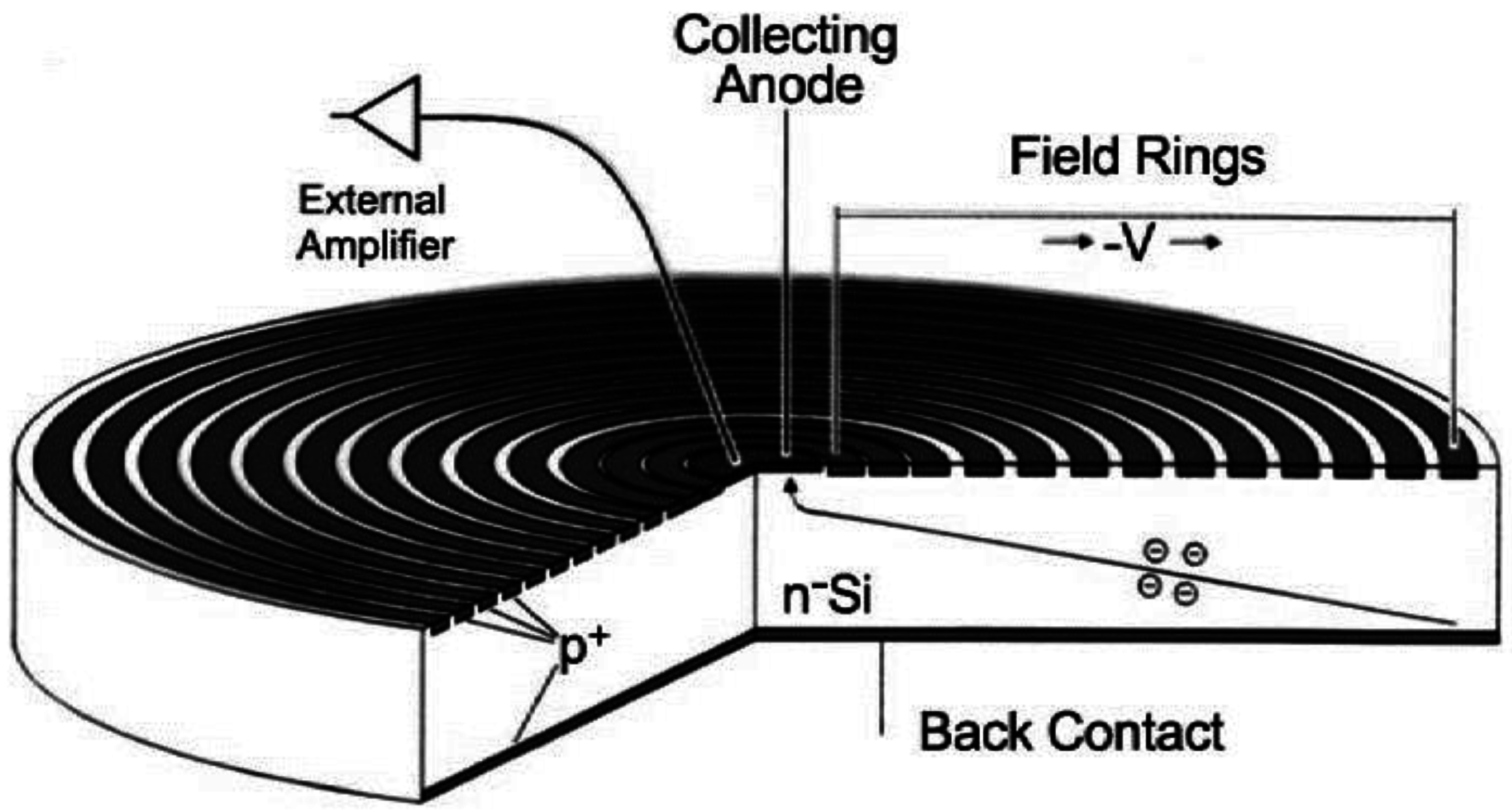
Figure 1, where the drift field, which sweeps light-generated electrons to the anode, is created by placing a voltage drop over a cathode on the anode side of the wafer [
19]. The cathode on the opposite side of the wafer, forming the light-entrance window, is biased at a constant voltage designed to assure depletion of the whole wafer between the cathodes and under the anode. As opposed to this, an SDD operated with the same constant voltage on both cathodes was proposed in [
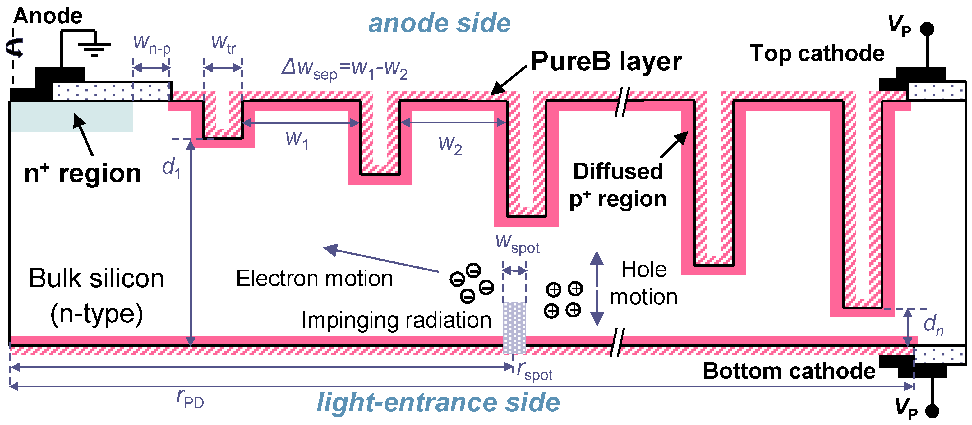
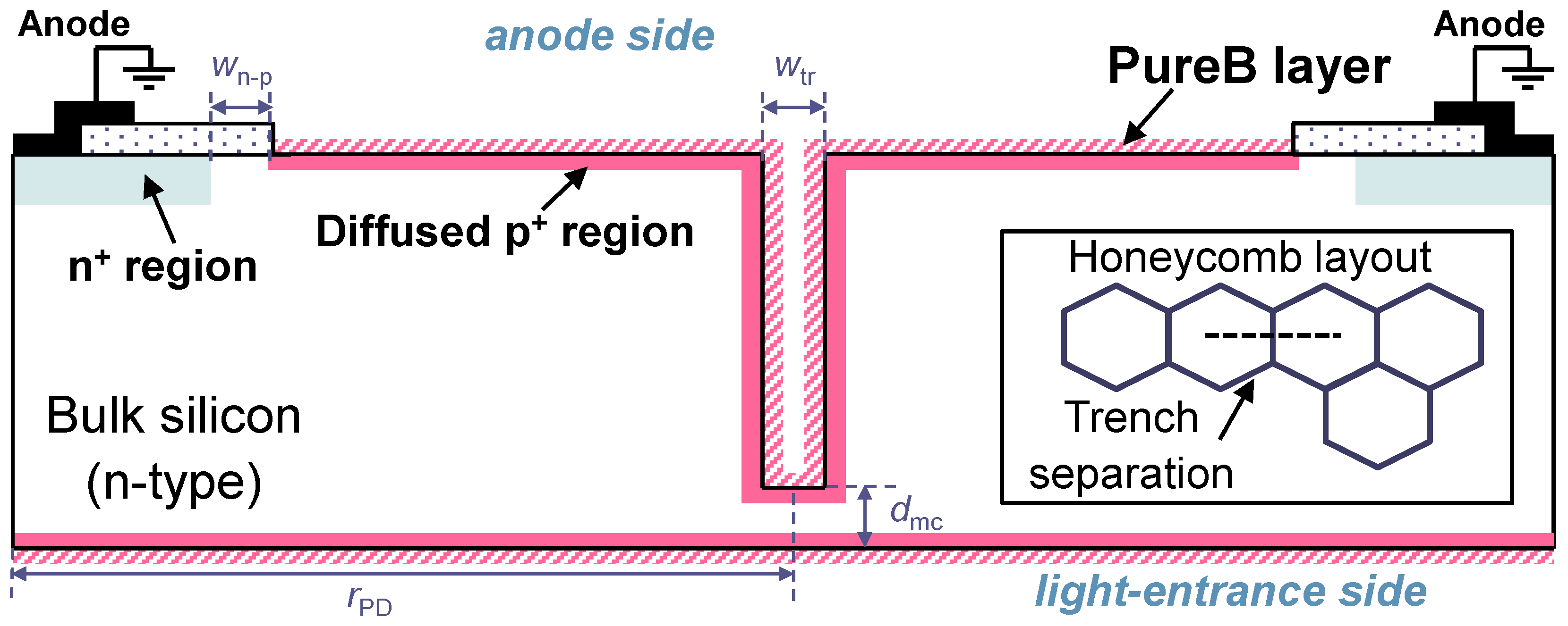
20]. In this design, a built-in drift region is obtained by tapering the semiconductor material between the cathodes, which has the disadvantage of reducing the photo-sensitive volume for high-energy light detection. In the present paper, a similar approach is taken but the large loss of photo-sensitive volume is circumvented by only removing material in narrow trenches etched to different depths in the Si, as shown in
Figure 2. The constant voltage that is then needed to obtain a suitable drift field cannot be predicted by simple analytical calculations and is investigated here by simulations. These are also used to compare the performance of this trenched drift detector (TDD) to conventional SDDs, such as the one shown in
Figure 1. To discern between the two designs in the following, the SDD made in non-etched bulk Si will be referred to as a BSDD (bulk-silicon drift detector).
Silicon, as a material, can be used directly as an X-ray radiation detector for detection of photons in the energy range from 30 eV to 30 keV [
4]. The upper limit of 30 keV is defined for 1-mm-thick silicon wafers for which approximately 25% of the 30 keV photons are absorbed inside the wafer. This is still sufficient for most applications and the wafers are available on the market with the necessarily very high resistivity. However, most SDDs have been fabricated on the more accessible 300–500 µm thick silicon wafers which decreases the absorption efficiency for high X-ray energies. The lower energy limit is set by the absorption in the layers above the photosensitive region, called dead layers, at the light-entrance side of the detector. An exceptionally thin dead layer of only a few nm is offered by PureB photodiodes that have been extensively used for soft X-ray detection (the 13.5 nm extreme ultraviolet (EUV) wavelength) as well as vacuum UV light and low-energy electron detection down to 200 eV [
21,
22]. This technology is proposed here for forming the p
+ regions since it has been demonstrated to deliver an ideal coverage of the Si and equally good diode performance on Si surfaces created by both wet and dry etching of trenches and cavities [
23,
24].
The main attraction of SDDs is that they have a very low capacitance at the anode where the signal charge is collected, in the range of a few tenths to hundreds fF, and the photosensitive area of the device can be scaled up without increasing the size of the anode. Since electronic noise at short shaping times is proportional to capacitance, the SDD yields much lower noise, giving better energy resolution and high count rates [
25]. To profit from this low-noise aspect, it is important to have a low dark current. There are two dominant components of the dark current: the bulk leakage and surface leakage current. The bulk leakage current is minimized by using high-quality high-resistivity Si wafers with very low carrier recombination lifetimes or by lowering the operating temperature of the device. Surface leakage current is caused by the defects at the interface between silicon and other materials. These defects can be created during the fabrication of the p
+ regions, and the SiO
2/Si interfaces used for isolation always have a certain amount of interface traps that ideally are in the 10
10 cm
−2 range. Surface leakage also benefits from a decrease in operating temperature but, nevertheless, it can be several times higher than the bulk leakage current [
26] and consequently determines the total leakage current. In BSDDs such as the one illustrated in
Figure 1, the voltage across the anode side of the device is created by a set of concentric p
+ rings that are biased through a voltage divider. The rings are separated by dielectric isolation, with the Si surface itself being covered by high-quality SiO
2. One of the main concerns during operation is the degradation of any depleted SiO
2/Si interface regions during irradiation. To minimize the area of such regions, floating guard rings are often implemented. The isolation interfaces between the p
+ rings are susceptible to radiation-induced damage from high-energy light that can reach the anode side of the detector. This can significantly increase the dark current. Therefore, a guard ring around the anode, called the sink anode, is often implemented to collect and drain away the electrons generated at the surface, thus reducing the sensitivity to interface damage but at the cost of also losing some fraction of the signal electrons [
14,
26,
27].
In the TDD, the basic structure of which is shown in
Figure 2, the two cathodes are both formed by continuous p
+ regions, thus reducing the area of the exposed oxide interfaces to the small region around the anode and the outer perimeter of the detector. These are the regions that are expected to be the main sources of leakage current. The fabrication of the PureB regions does not introduce defects in the Si, and the PureB/Si interface is ideally passivated [
28,
29]. Hence the PureB junction itself has ideal
I-V characteristics, also on trenched surfaces [
23,
24], and it is resistant to radiation damage. This has been tested extensively for soft X-ray (particularly 13.5 nm) and electron (200 eV–30 keV) irradiation [
30,
31]. For tens of micrometers-wide depletion of the bulk, the leakage current of PureB diodes has been found to increase with the depleted perimeter region and bulk volume size [
32]. On high-quality silicon material, dark currents well below 1 nA/cm
2 have been regularly obtained.
In the SDDs discussed here, the photo-sensitive region is in fact a depleted p
+np
+ reach-through diode across which the applicable voltage difference is limited by the flat-band voltage
Vfb. Above this voltage-difference a large current will flow between the two cathodes and create undesirable noise from associated generation-recombination electrons swept to the anode [
33]. In the TDD the voltage difference is zero, completely eliminating reach-through currents and currents flowing laterally through the cathodes. In the BSDD structure the spacing between the p
+ rings on the anode side of the detector is determined by the ability to fabricate resistors with high enough resistance values to keep the current flowing through them at a level that is so low that it will not influence the functioning of the read-out electronics.
In the simulations we also consider configurations where the SDDs are composed of an array of smaller drift detector cells. Such designs are used to provide a large sensitive area and low-noise performance, while moderate voltage drops maintain a high count rate. The individual SDD in such a multi-cell array usually has a hexagonal shape so that a honeycomb-like arrangement can be used to fully cover the Si with detector cells. Each cell must contain an anode, but only one guard-ring structure is needed at the outer edge of the total array, since all the elements are at the same potential. Multi-cell drift-detector structures suffer from cross-talk between adjacent cells [
34,
35]. Also, the peak-to-background ratio is decreased in a 90-µm-wide area between cells [
35]. Cross-talk can be reduced by applying a radiation mask [
35]. On this point the simulations show that the TDD multi-cell detector can significantly reduce the area where cloud splitting occurs between adjacent cells, thus minimizing the optical cross-talk.
2. Trenched Drift Detector Concept
Ideally, the maximum potential difference that can be created over the drift field in the BSDD is given by [
1]:
where
q is the elementary charge,
εSi is the dielectric constant of Si,
dwafer is the thickness of the Si wafer, and
ND is the doping concentration of the n region. In addition, the depletion approximation has been assumed and the influence of the relatively small built-in junction voltage has also been neglected. With 0 V on the anode, the bulk n region is fully depleted by biasing the p
+ region on the entrance window side with the voltage
Vfb. On the anode side, there is then freedom to choose the bias voltages
Vinn and
Vout on the inner and outer p
+ rings, respectively, up to a voltage of 2
Vfb. For the TDD, the voltage placed on the cathodes must minimally be equal to ¼
Vfb to fully deplete the unetched bulk n region. Where trenches have been etched leaving a Si region of thickness
di, a smaller voltage, proportional to
di2, is needed to provide the flatband condition. Assuming a maximum Si thickness
dwafer adjacent to the anode and an outer trench leaving almost zero Si thickness, the maximum achievable potential over the drift field can be approximated by:
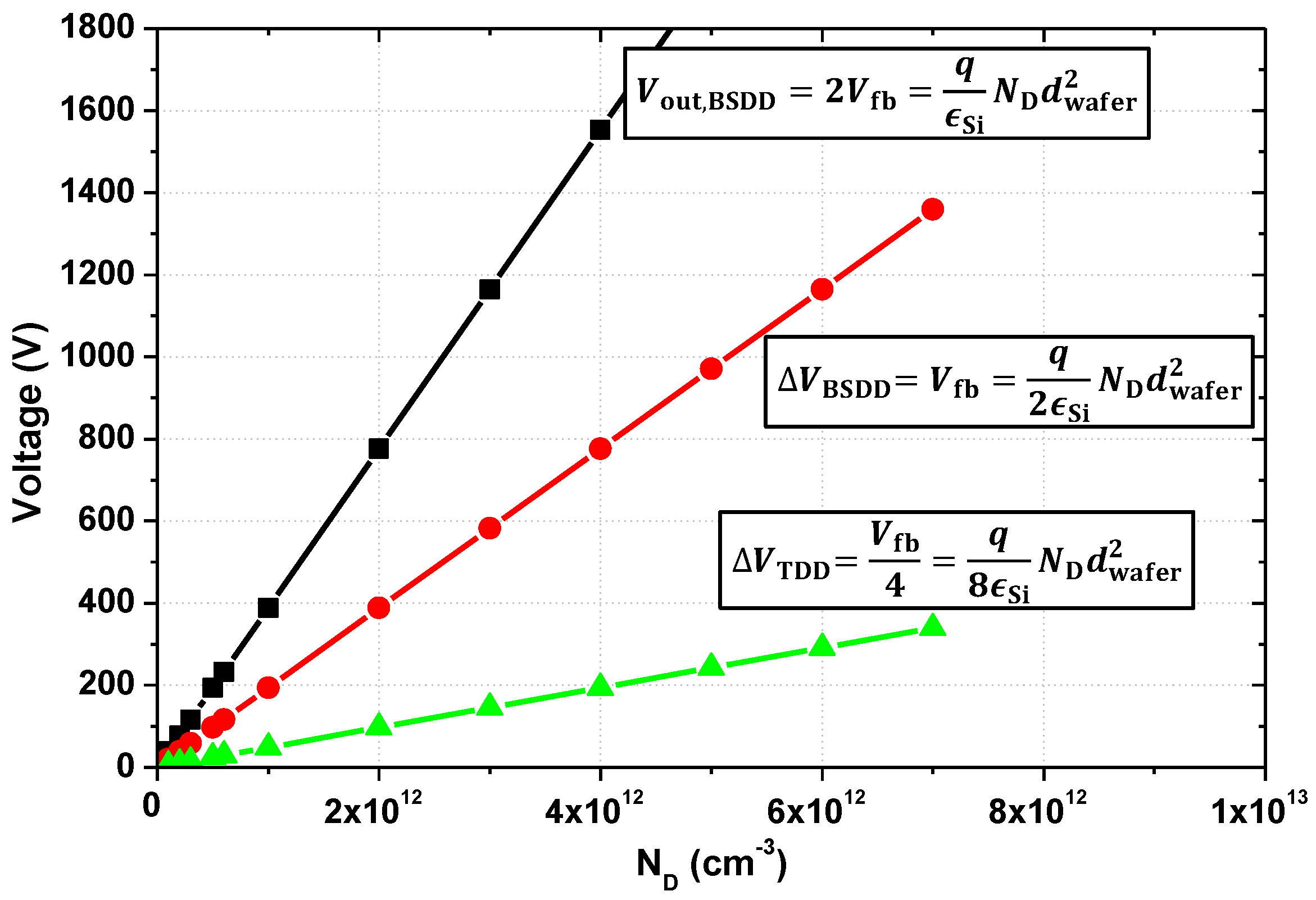
These relationships are plotted in
Figure 3 as a function of wafer doping for a 500 µm thick wafer. It is evident that for a given n-doping level, the BSDD structure permits a four times higher drift field than the TDD. In Si, breakdown voltages higher than about 1000 V are generally not used. In the BSDD the applied voltage is two times higher than the induced drift-field potential, so in the chosen example this would limit the doping level of the BSDD to about 2 × 10
12 cm
−3. In reality, a
Vout lower than 2
Vfb can be applied at the price of lower drift field. In contrast, in the TDD, the size of the drift-field is determined by
ND and the device topography: applying a higher biasing than needed for full depletion will not increase it. From this simple calculation, a drift field of 80 V/cm is found for a detector radius of 3000 µm and a wafer doping of 5 × 10
11 cm
−3. Higher doping can be used to increase the drift field at the price of higher applied voltage.
In the following sections the simulations of TDDs with several trenches of varying depth show that the voltage that must be applied to create a reliable drift field cannot be predicted by simple analytical formulations: a higher voltage than ¼Vfb must be applied to prevent potential wells. Moreover, a number of geometrical parameters must to be properly adjusted to keep the required voltage as low as possible. For simulation simplicity the width of each trench was fixed at wtr = 10 µm and the distance between the trenches was organized so that wj = wi − ∆wsep, with i = 1, …, n, j = i + 1, and n is the number of trenches. The increase in the depth of the trenches was chosen to be constant and defined by n and the Si thickness left under the first and last trench, d1 and dn, respectively. Other parameters that were varied are the distance between the n+ anode contacting-region and the adjacent p+ region, wn-p, and the radius of the active photodiode region, rPD. The analyzed bulk doping concentrations ND in the range of 5 × 1012 cm−3 down to about 5 × 1011 cm−3 were chosen to correspond to resistivities of 1 kΩ·cm–10 kΩ·cm that are commonly available for high-ohmic wafers.
2.1. Electrostatic Optimization of the TDD Structure
Commercially available Sentaurus TCAD software from Synopsys was used for the simulations and the analysis of the drift detector structures [
36]. In the simulations, based on experimental results for PureB diodes from 700 °C boron depositions [
37], the PureB p
+ region is simulated as a high-doped region with peak concentration at the surface of 2 × 10
19 cm
−3 and a Gaussian doping profile. The pn-junction depth of the boron-diffused region for
ND = 5 × 10
11 cm
−3 is assumed to be 50 nm. A circular TDD geometry is assumed in all simulations. If not stated otherwise, the interface is simulated without interface charge and interface traps.
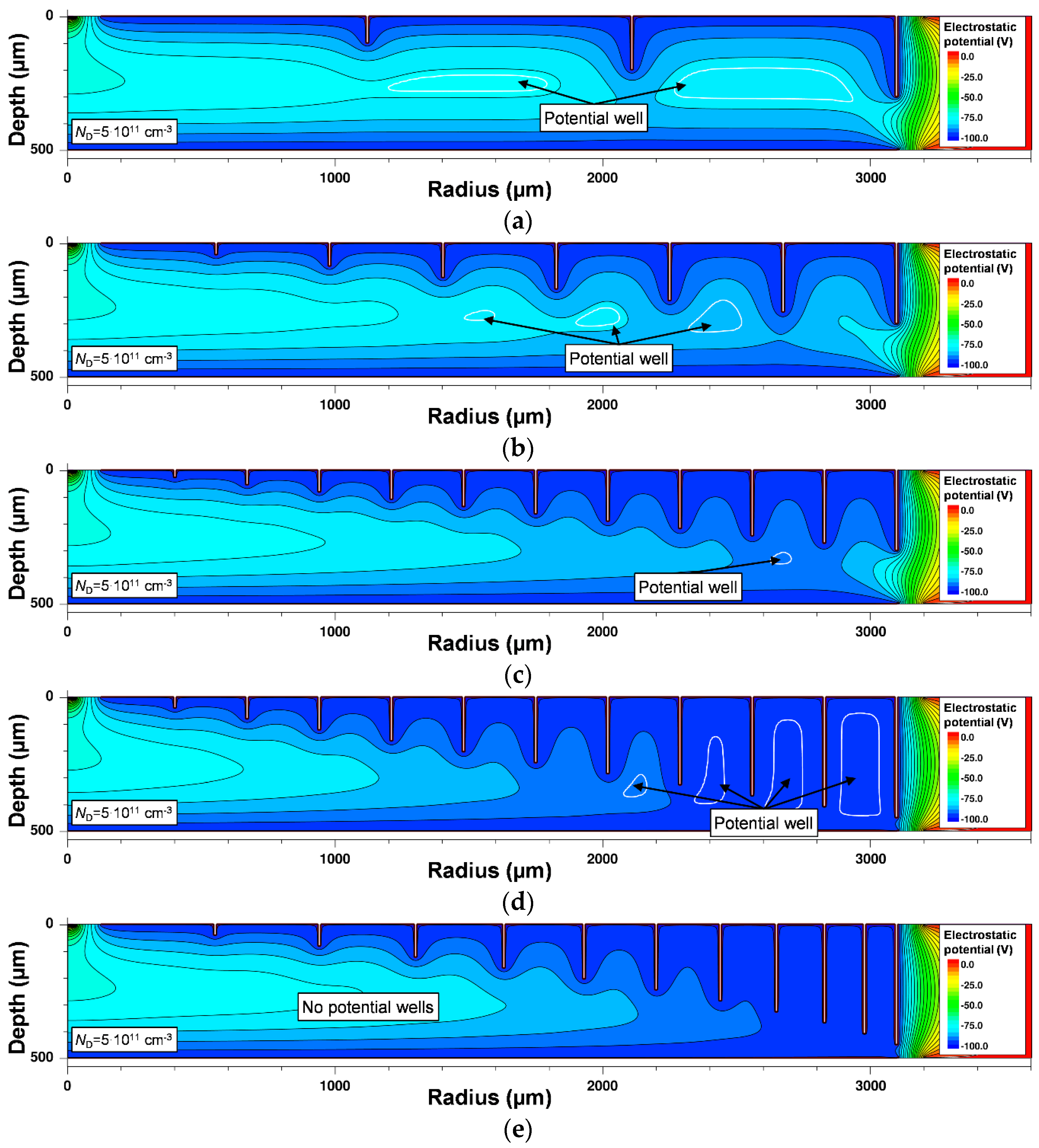
First, a TDD is simulated with
d1 = 500 µm,
wn-p = 100 µm,
rPD = 3100 µm, and
ND = 5 × 10
11 cm
−3. The anode contact and the periphery are grounded while the anode- and light-entrance side p
+ contacts are reverse biased. The electrostatic potential distribution of the structure with different trench depths is plotted in
Figure 4a–e. The bias voltage of the p
+ regions,
Vp, is −100 V, which is much higher than the voltage ¼
Vdepl = 23 V necessary for depleting the wafer. While this does not influence the bulk drift field, this high bias is necessary for depleting the inner and outer perimeters of the device. The electrostatic potential distribution in structures with non-optimized trenches is shown in
Figure 4a–d. In these structures, there are potential wells that will accumulate any charge absorbed in the vicinity of the potential well, and this will lead to poor responsivity. In
Figure 4a, with
n = 4,
dn = 200 µm, and Δ
wsep = 0, a large potential well is visible between the trenches. This situation can be ameliorated by increasing
n to 8 or 12, as shown in
Figure 4b,c. However, if
dn is decreased from 200 µm to 50 µm, which increases the size of the drift field and gives a better separation of the active part of the structure from the peripheral region, the region between the last few trenches will nevertheless be left with potential wells. This can be alleviated by optimization of Δ
wsep. A structure without potential wells is achieved for the parameters:
n = 12,
dn = 50 µm, Δ
wsep = 30 µm. In
Table 1, parameters of TDDs that will result in devices without potential wells are given for various
n,
dn, and Δ
wsep values. For an
n of 4 or 6, the proposed biasing of the trenched drift detector could not eliminate potential wells in the structure.
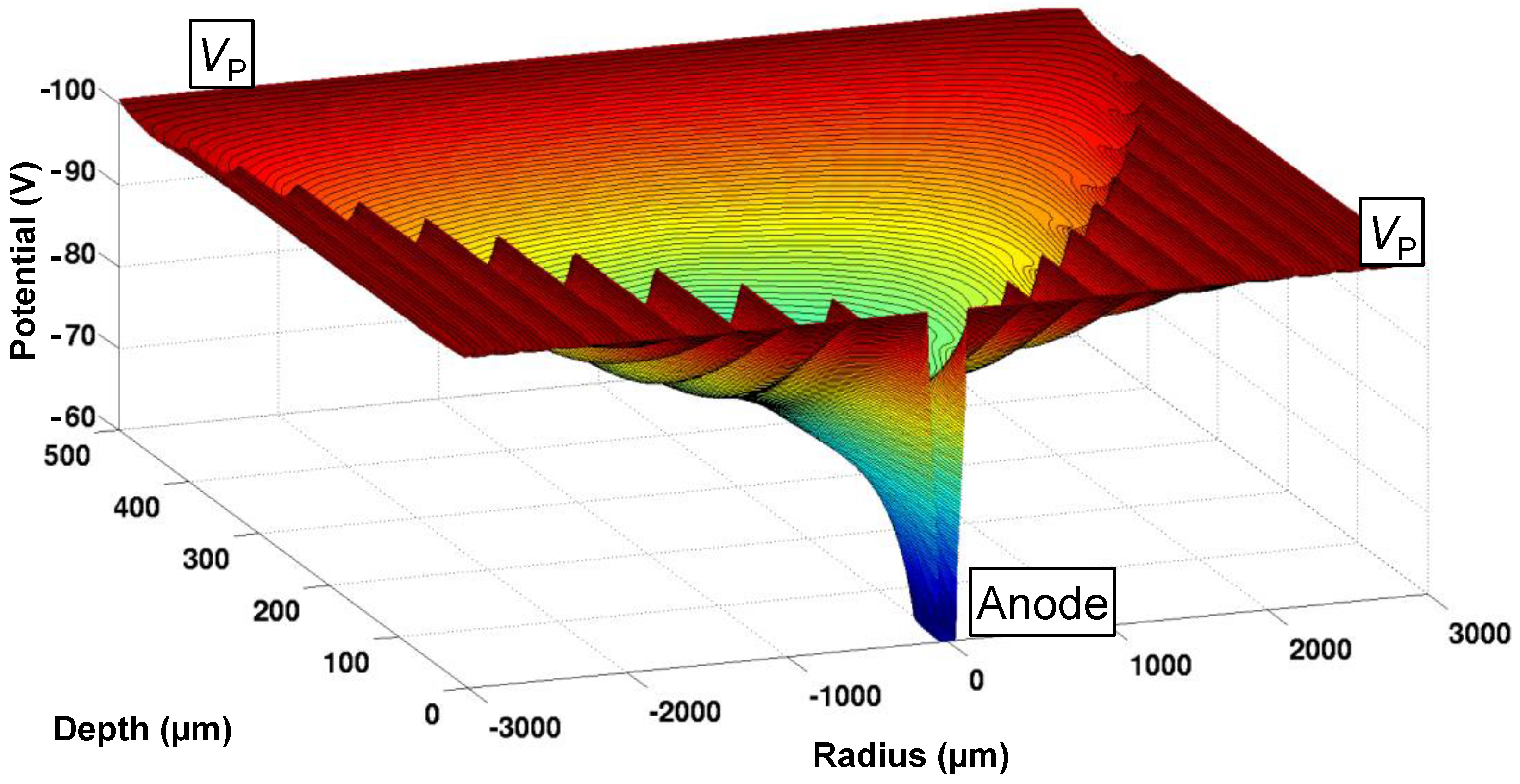
The potential distribution for the optimized structure of
Figure 4e is plotted in
Figure 5 and displays a fully-depleted drift region with no potential wells. The optimized parameters are
n = 12,
dn = 50 µm, and Δ
wsep = 30 µm for
ND = 5 × 10
11 cm
−3. Most of the potential drop is situated between the anode and anode-side p
+ region. However, the potential distribution in the drift region is steadily decreasing across the whole active region.
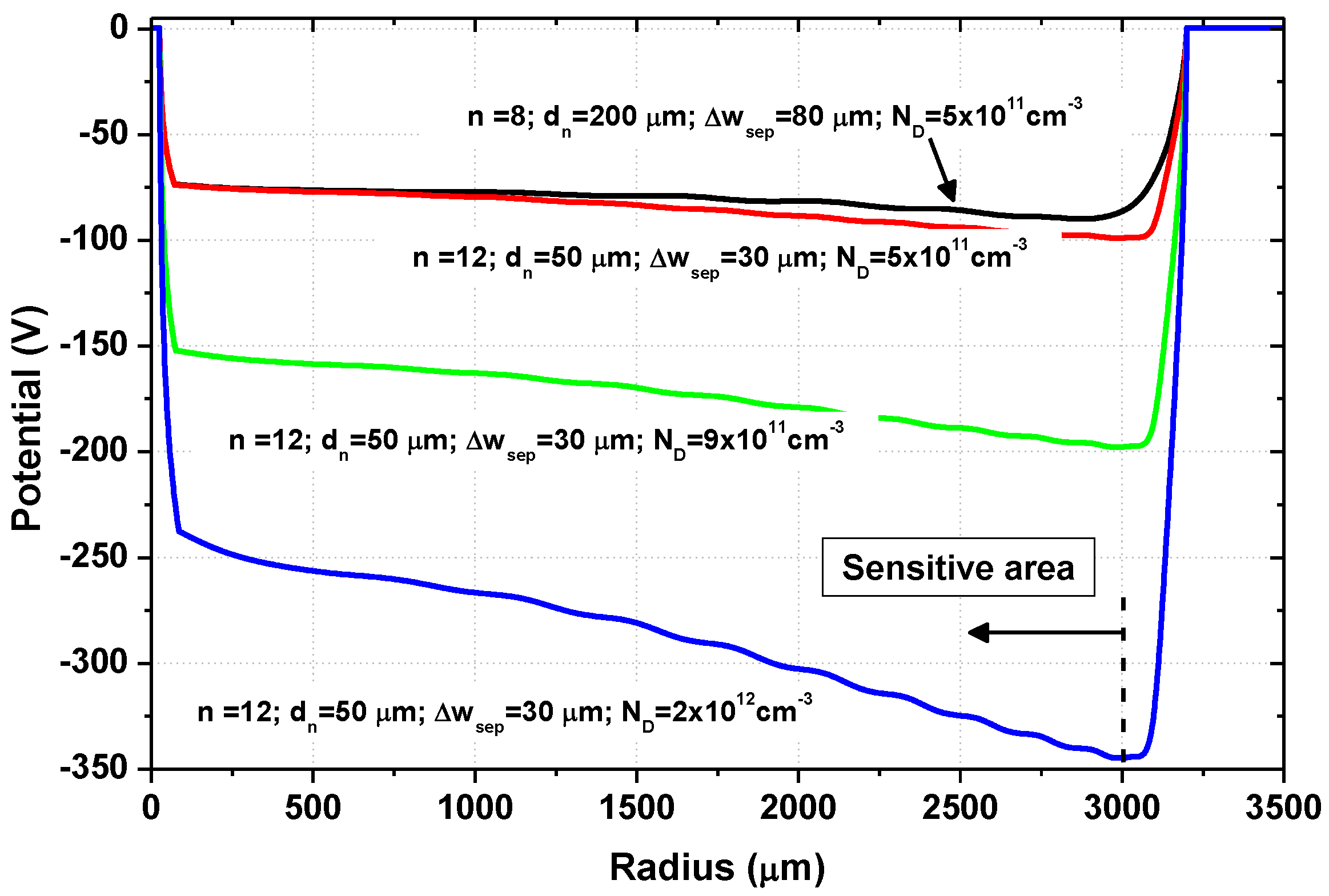
The electric potential along the drift valley in a TDD is plotted in
Figure 6 for different geometrical configurations and biasing optimized to give a drift region without potential wells. At the outer perimeter, the junction to the n region induces a potential minimum in the drift valley that will determine the usable sensitive surface of the detector. Light impinging at a radius past this point will be swept to the peripheral contact. For the upper curve in
Figure 6, with
n = 8,
dn = 200 µm, Δ
wsep = 80 µm, the total sensitive region has a 120 µm smaller radius than the neighboring curve, with
n = 12 and Δ
wsep = 30 µm. This is due to the larger depth of the outer trench, but even with
dn = 50 µm the potential difference ∆
VTDD to move the electrons is only 25 V and the drift field is about 85 V/cm. This will result in long drift times for collection of the charge generated at the outer edge of the active region. Higher fields can be achieved by increasing the bulk doping, as shown in
Figure 6 for 9 × 10
11 cm
−3 and 2 × 10
12 cm
−3. In order to have full depletion without potential wells, the bias voltage is also increased to −200 V and −350 V, respectively. In the last case,
wn-p had to be increased to 150 µm to avoid breakdown of the n
+–p
+ junction on the anode side of the detector. Smaller
wn-p could be maintained by adding floating guard rings at the periphery of the high doped regions. The potential differences in the drift region for
ND of 9 × 10
11 cm
−3 and 2 × 10
12 cm
−3 are 45 V and 106 V, respectively, resulting in drift fields of ~160 V/cm and ~370 V/cm, respectively.
Even with suitable guard rings, the high field across the junction at the anode can be a disadvantage for the TDD structure as compared to the BSDD, where
Vinn can be kept as low as 0 V. A high field combined with the presence of irradiation events could promote impact ionization events that create extra parasitic electron currents and enhance interface degradation. The degree to which this counteracts the advantage of not having any oxide interface areas on the rest of the cathode surface will depend on the exact implementation and application of the detector. For example, a droplet-like design developed by PNsensor [
38] completely avoids irradiation of the anode region.
2.2. Transient Simulations
Transient simulations were performed by illuminating the light-entrance side of the detector with X-rays that are varied in energy and intensity. The width of the illumination spot (
wspot) was 0.1 µm and it was placed at various distances
rspot from the center of the photodiode, as indicated in
Figure 2. The exposure to the X-rays was given a Gaussian time dependency with a variance equal to 10
−15 s. The absorption coefficients for silicon were included in the simulator for energies up to 50 keV [
39], while the internal quantum efficiency was adjusted to accommodate the mean energy of about 3.6 eV to produce one electron-hole pair.
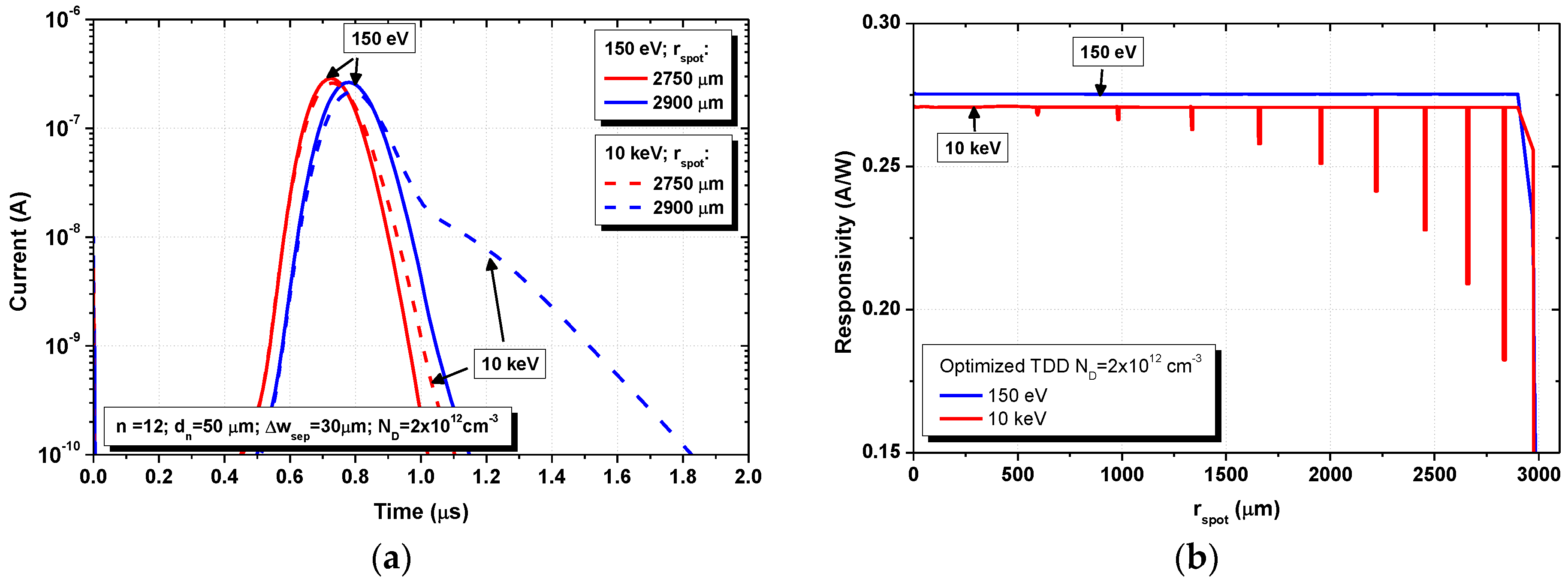
Transient responses of the anode current are plotted in
Figure 7 for different TDD structures and positions of the illumination spot. The light energy was 150 eV and the intensity 5 × 10
6 W/cm
2. The amount of generated charge increases with increasing radial position due to the cylindrical symmetry of the simulation setup. The time it takes to achieve the maximum current at the anode contact (
tImax) increases with increasing
rspot. However, for a TDD with higher bulk doping, the higher drift field will decrease the total collection time. For
rspot = 2000 µm,
tImax decreases from 2.59 µs to 1.36 µs, and 0.54 µs for
ND going from 5 × 10
11 cm
−3 to 9 × 10
11 cm
−3 and 2 × 10
12 cm
−3, respectively. TDDs are sensitive to X-ray detection across almost the whole radius of the active region, with reduction in responsivity being caused only by the trenched areas.
The vertical drift field in the regions between the trenches at large radii is low. This can deteriorate the timing performance of the TDD device for high-energy detection since the electrons absorbed in this region will move more slowly to the horizontal drift-field region below the trenches. The TDD device performance for high-energy detection is analyzed by also illuminating with X-rays with an energy of 10 keV. The width of the illumination spot was 0.1 µm and it was placed at distances
rspot of 2750 µm (between trenches Nos. 9 and 10) and 2900 µm (between the trenches Nos. 10 and 11), respectively. The transient simulations were performed for the optimized TDD structure with
ND = 2 × 10
12 cm
−3 and are shown in
Figure 8a. For
rspot = 2900 µm, a distinct tail in the transient response is observed which is attributed to the slow drift of the generated electrons in the region between the trenches. Responsivity simulations are performed for optimized TDD structures with
ND = 2 × 10
12 cm
−3 and plotted in
Figure 8b. In the responsivity analysis, steady-state simulations were performed with 0.1-µm-wide light spots of energy 150 eV and 10 keV and intensity of 1 W/cm
2. Near-ideal responsivity is found except where the silicon is etched away to form the trenches and where the drift-field potential directs the generated electrons to the periphery of the detector.
2.3. Comparison of TDDs to BSDDs
A conventional BSDD structure was simulated with parameters that are typical for these devices:
ND = 5 × 10
11 cm
−3,
wn-p = 100 µm, and
rPD = 3100 µm. The simulated BSDD and TDD are comparable except that on the anode side of the BSDD the drift field was created by replacing trenches by a patterned p
+ region. This requires 20 p
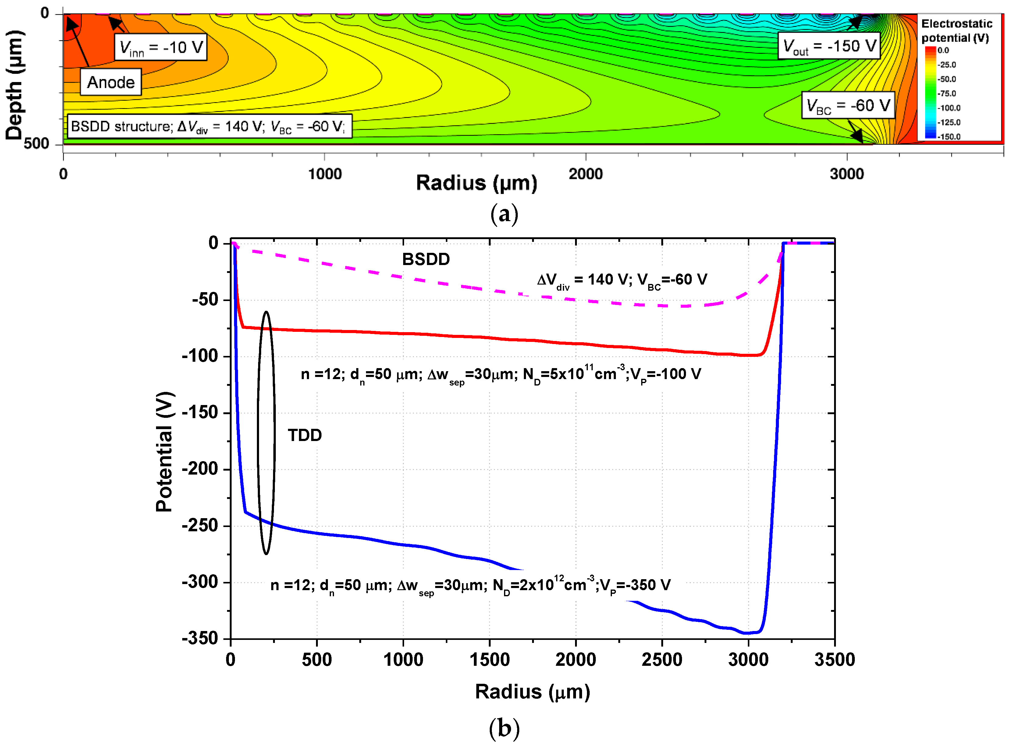
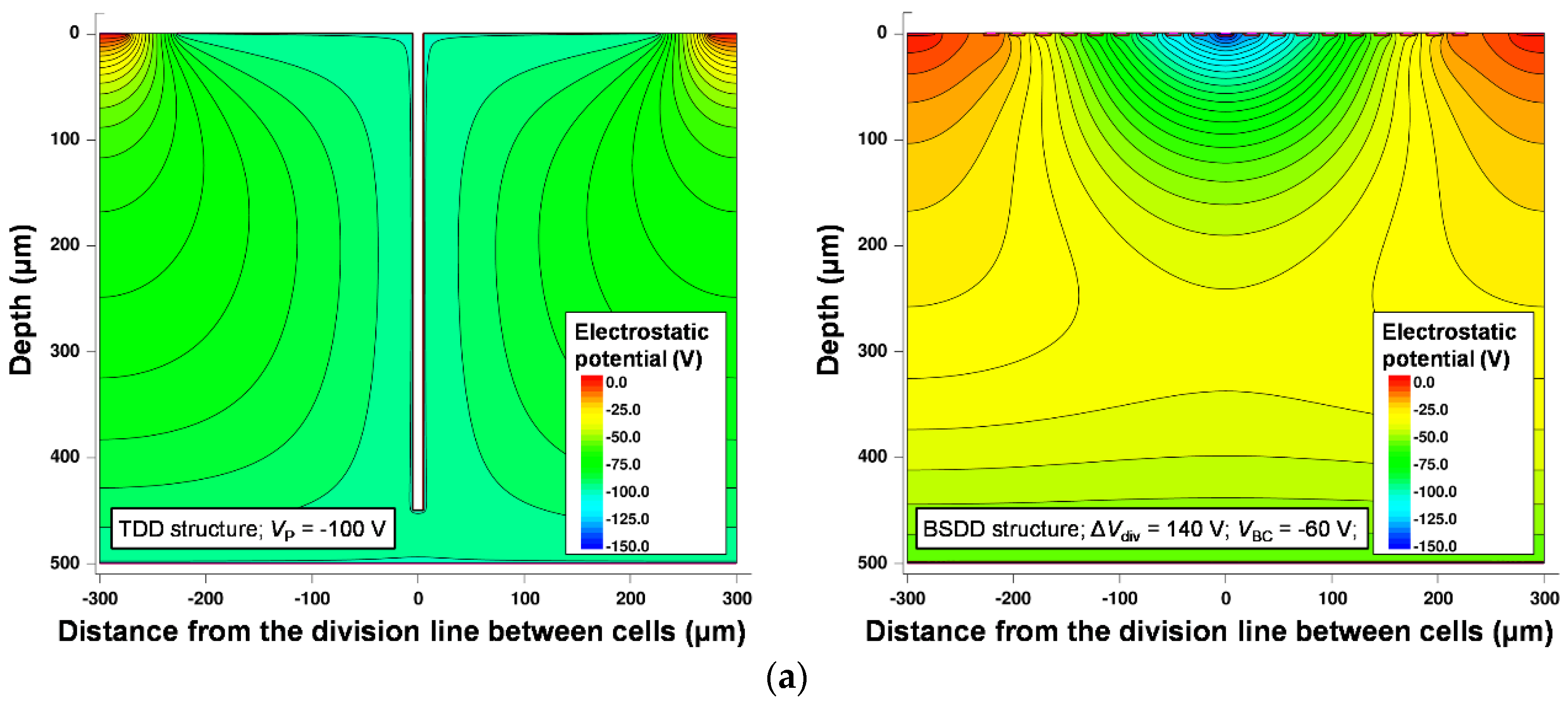
+ rings that are reversely biased through a voltage divider. The electrostatic potential distribution for this BSDD is shown in
Figure 9a. On the light-entrance side, the p
+ region is reversely biased to
VBC = −60 V, while on the anode side voltage is divided between
Vinn = −10 V and
Vout = −150 V, giving a voltage drop of
Vdiv = 140 V. This reverse biasing is chosen to fully deplete the BSDD and achieve a maximum drift field without punch-through.
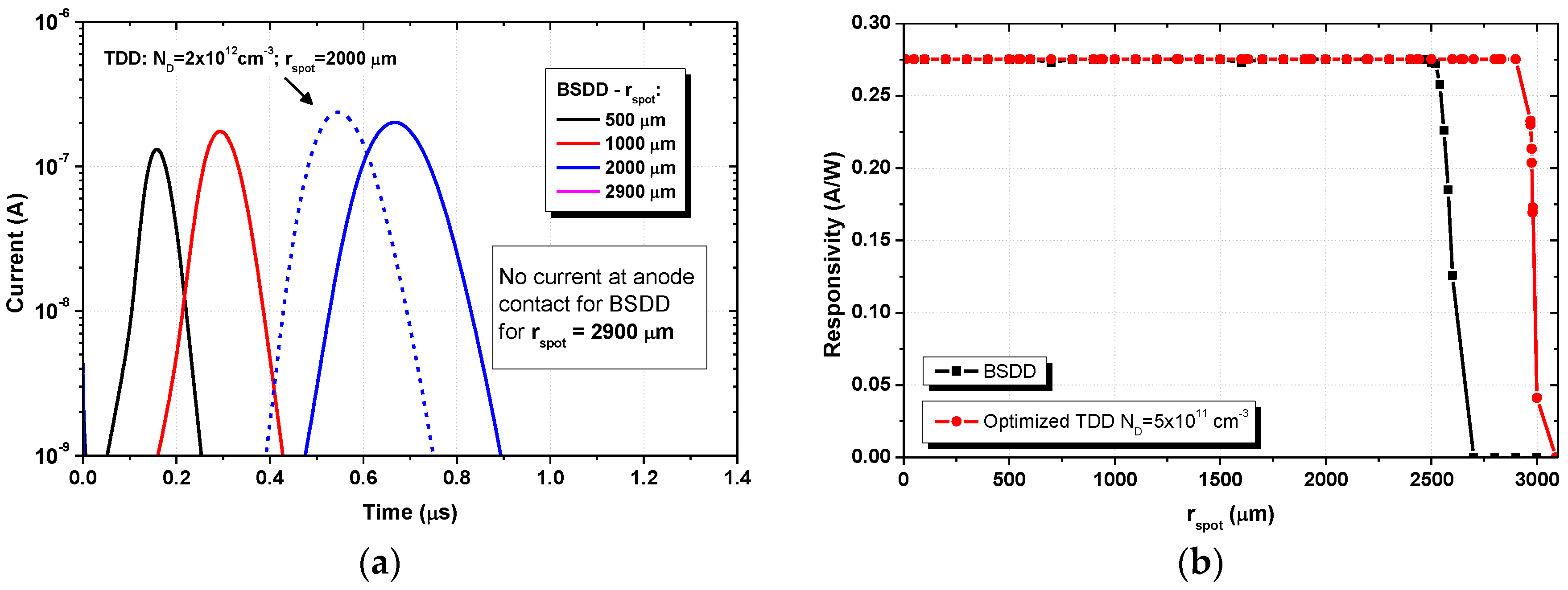
A comparison of the electric potentials along the drift valley is shown in
Figure 9b. For the simulated BSDD structure, a drift field of ≈210 V/cm is achieved. However, the BSDD has a potential minimum situated at a radius of 2600 µm, which limits the sensitive area of the device. This is in contrast to the TDD that can be used for detection of X-rays entering practically the whole active region.
The transient response of the TDD and BSDD structures was simulated for a 150 eV light spot with an intensity of 5 × 10
6 W/cm
2 impinging on different positions across the light-entrance window. The TDD was optimized with
ND = 2 × 10
12 cm
−3 and the simulation results are plotted in
Figure 10a. The BSDD structure has a larger drift field, so
tImax decreases and the generated charge will be collected more quickly. However, the optimized TDD with
ND = 2 × 10
12 cm
−3 can provide a comparable collection time. Moreover, it appears that the radius of the sensitive area of the BSDD is 500 µm smaller than that of the TDD. The responsivity across the BSDD photodiode is shown in
Figure 10b, for which steady-state simulations were performed with a 10-µm-wide light spot of energy 150 eV and intensity 1 W/cm
2. There is a sharp decrease in responsivity at
rPD = 2500 µm, while for the TDD structure with
ND = 5 × 10
11 cm
−3, the responsivity does not decrease before
rPD = 2950 µm. This confirms that the radius that can be used for detection is increased by almost 500 µm in the TDD structure.
The impact of interface traps on the anode dark current of BSDDs and TDDs was also evaluated by performing electrostatic simulations with different amounts of interface states in the oxide regions. The effects of extra current generation during irradiation due to, for example, the influence of light-induced impact ionization events is not taken into account but could possibly play a role when the electric field over an oxide interface is high. This situation for the TDD anode junction was discussed in
Section 2.1. In general, exposure to X-ray radiation of photons below 250 keV, as is typical for SDDs, generates ionization damage in oxide layers, which results in the increase in concentration of the interface traps. The elimination of a large part of the interface oxides is expected to give TDDs an advantage in radiation hardness in comparison to BSDD devices that are not equipped with a sink anode. The type and the concentration (
NT) of the interface traps was varied from the ideal value of 10
10 cm
−2 up to 10
12 cm
−2, while the capture cross section of the traps was constant and set to be 10
−15 cm
2 for both electrons and holes. All the traps have a midgap energy. Carrier recombination lifetimes for both electrons and holes of 10
−3 s were assumed. Simulation results of the anode dark current (
Idark) for both the BSDD and the optimized TDD structure are given in
Table 2. For comparison, the dark current for a structure without interface traps was also simulated. The maximum anode dark current increase of 3.5 nA was achieved for a TDD with a donor-type trap concentration of 10
12 cm
−2. This is only a 34% increase of the anode dark current as compared to not having any traps. In contrast, for the same trap type and concentration, the dark current increase for the BSDD is 240.6 nA, which is two orders of magnitude higher. Due to the continuous p
+ regions on both sides of the structure, the TDD is inherently resistant to surface dark currents and a sink anode would not be necessary if current generation effects during high-energy light illumination do not dominate. The oxide surface area of the simulated BSDD is 0.19 cm
2, while the TDD surface area is only 0.0005 cm
2. On the other hand, the TDD has a larger p
+ surface area due to the trenched region. For the multi-trench device of
Figure 4e, the total p
+ area on the anode side is increased by about a factor of 3. This will not change the dominating component of the dark current, the hole current, which is determined by the doping and size of the n regions, but the size of the electron component is proportional to the p
+ area. Nevertheless, the low electron saturation current means that the corresponding increase in dark current will be insignificant.
3. Multi-Cell Drift Detector Array of TDDs
TDDs can be used as building blocks in multi-cell drift detector arrays. Since the drift elements in an array have smaller dimensions, the number of trenches to fully deplete the sensitive area and also prevent the formation of potential wells can be decreased. This has obvious advantages for the device fabrication. To understand the consequences for the device performance, a cell with only one trench to set the drift field was simulated. This was at the same time the outer trench of the cell and could be used to separate the individual segments of the array. A cross section of the simulation structure used to examine two adjacent segments is shown in
Figure 11, along with the array layout that could be used for an optimal packing density with maximum use of the Si area for detection. The cells are chosen to be six-sided and placed in a honeycomb-like arrangement. Having all the p
+ regions biased at the same reverse voltage, which is made possible by the TDD design, would simplify the bonding and contacting layout of the device. In the simulations, the other parameters were
dmc = 50 µm,
wn-p = 50 µm,
rPD = 300 µm,
wtr = 10 µm, and
ND = 5 × 10
11 cm
−3. AC simulations of the proposed structure showed that the capacitance of each segment was 13 fF, which would make the electronic noise of each cell low.
A reverse bias of −100 V was applied to the p
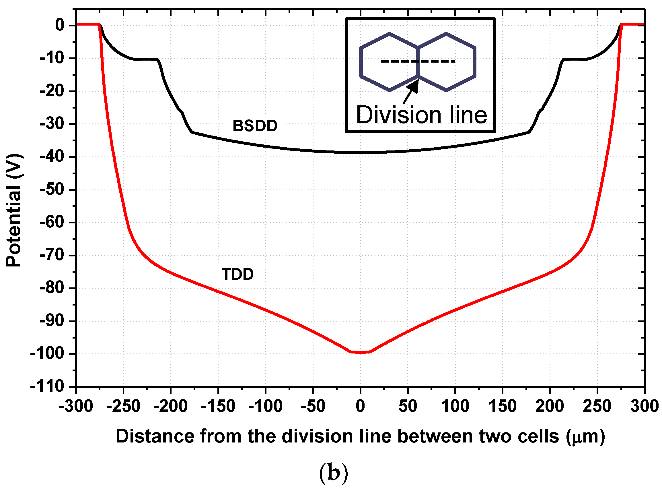
+ regions which resulted in the full depletion of both segments. The electrostatic potential distribution for multi-cell TDD and BSDD devices are compared in
Figure 12a; the electric potential along the drift valley is plotted in
Figure 12b. The BSDD cell was patterned with p
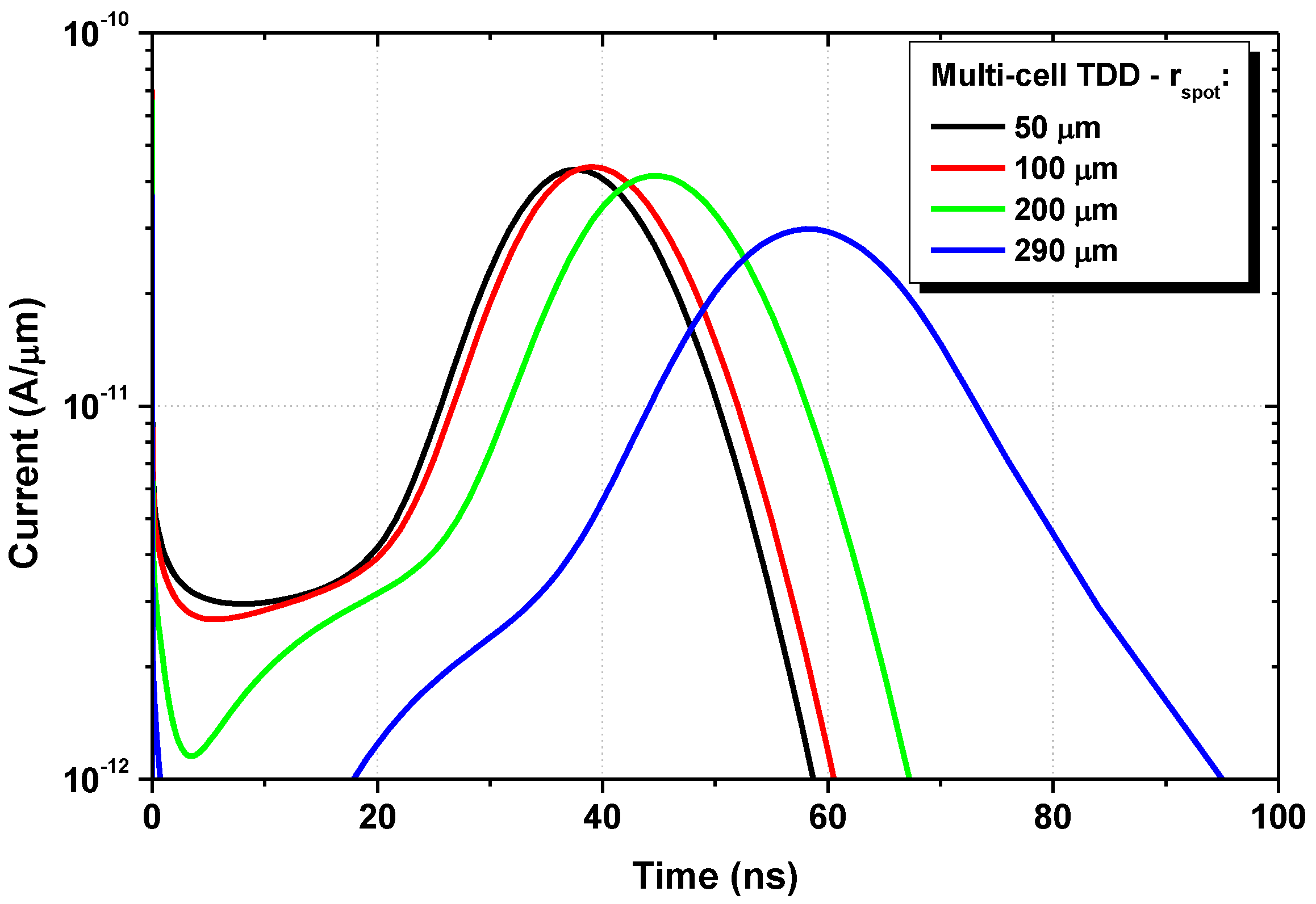
+ rings the anode side of the wafer. The TDD has a much higher drift field of almost 1000 V/cm, which will give short drift times and fast charge collection. The trench electrically separates neighboring cells in the array and provides a very narrow 10-µm-wide strip between the cells where the drift field is small. In contrast, in the BSDD structure, the area between two segments where the drift field is small extends up to 100 µm on each side of the cell division line. This area will be responsible for long collection times and cross-talk between two segments since the charge generated in this region can easily end up being split between the segments. Fast collection times in the multi-cell TDD are confirmed by the transient simulations shown in
Figure 13. The total charge collection at the anode contact for
rspot = 290 µm is seen to be under 100 ns, which could theoretically result in count rates up to 10 Mcps, ignoring the processing time for electronic read-out.
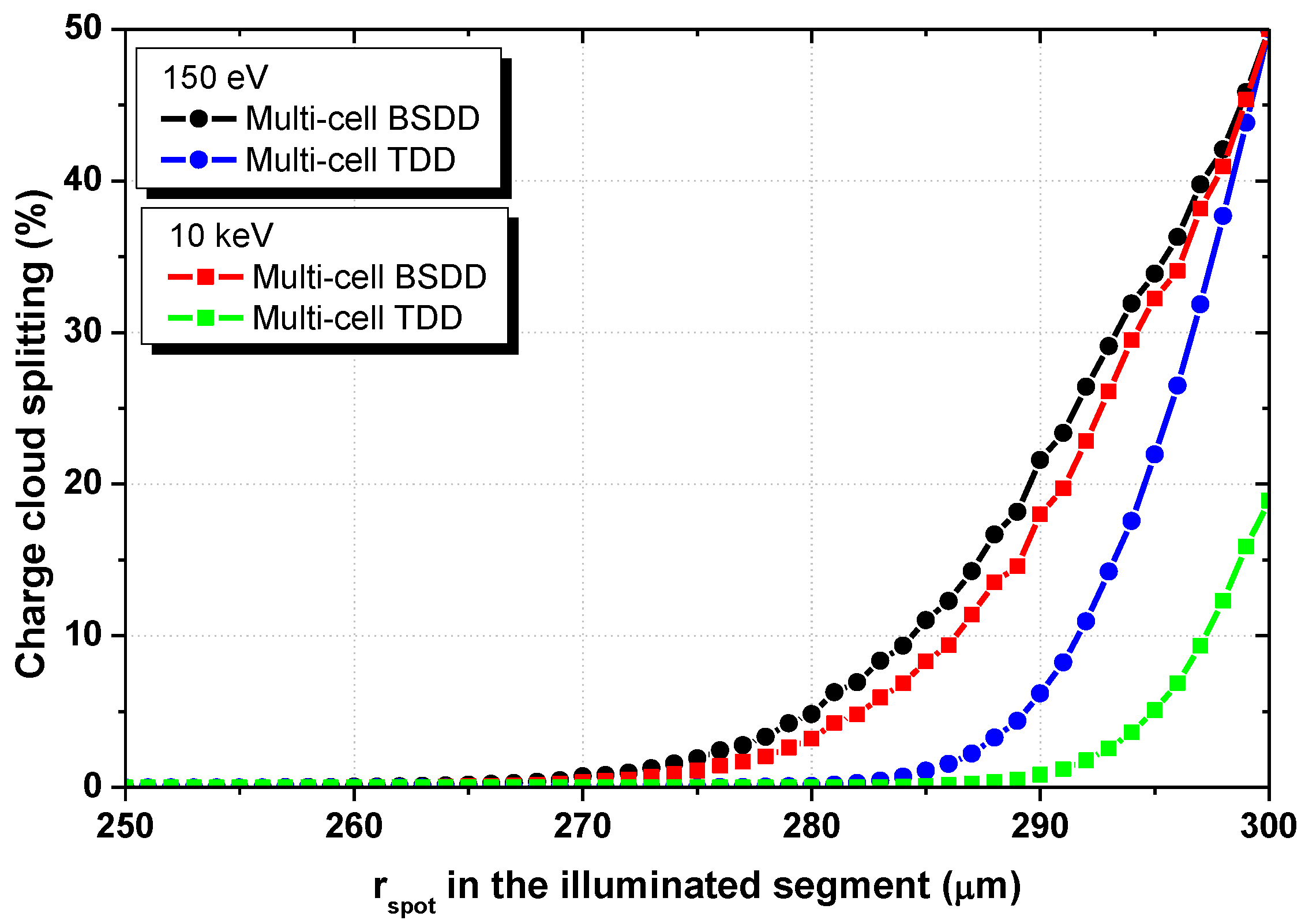
The cross-talk between two adjacent cells was also analyzed by performing simulations where only one segment was illuminated but the resulting anode photocurrent was monitored on each of the cells. The ratio of the two anode currents (non-illuminated divided by illuminated cell current) was calculated and is plotted in
Figure 14. For 150 eV light energy, the charge cloud in the BSDD is split between the cells when the illumination spot is within a 35 µm-wide strip around the cell edge, while this is only 20 µm for the TDD. This is reduced further for higher light energies, as seen from the example using 10 keV energy. These results show that for a multi-cell BSDD array, a strip of around 40 µm wide between the segments cannot be used, assuming that 10% charge splitting to an adjacent segment is acceptable. This is in agreement with the results reported in [
35]. Using the TDD will decrease this area by a factor of 2 and only 20 µm of the surface between each segment will suffer from the optical cross-talk. At the same time, for higher X-ray energies the trench will provide screening similar to what is achieved by the radiation mask proposed in [
35]. For high-energy radiation, the thin Si region of width
d2 below the trench will only absorb a small portion of the light. This will effectively reduce the amount of the photo-generated charge, thus decreasing the region susceptible to cross-talk to only 10 µm of the surface between each segment. Reduction of the trench width would further improve these values.
In the TDD, the cloud of electrons and holes created by high-energy photons can also be split between two adjacent cells if the photon transverses the trench while still actively generating events. Some signal electrons may also be lost in the trench but otherwise this splitting of the charge has the same effect on optical cross-talk as the mechanism described in the previous paragraph. Since the detection of the split charge is correlated in time, image processing with pattern reconstruction can be applied to reduce the impact on resolution.
4. Comments on TDD Manufacturability
The most critical processing step in the fabrication of TDDs is the etching of the trenches. As a result of the push towards manufacturable MEMS structures and through-wafer vias, deep reactive ion etch (DRIE) equipment has become available for etching the required hundreds of microns-deep trenches in Si with widths less than 10 µm [
40]. Controlling the depth of the trench is important for the TDD application and methods that make this possible within some tens of microns have been reported [
41]. For designs with several trench depths, to simplify the processing, more than one trench depth can be fabricated in a single etch step by using the fact that in small windows the trench etch-rate can be made slower than for larger windows [
42]. The coating of the trenches with PureB at a deposition temperature of 700 °C has already been demonstrated for both wet and dry etching of hundreds of microns-deep cavities [
23,
24]. The PureB diodes made in such cavities were ideal and it was demonstrated that the PureB has conformal coverage over rough surfaces composed of different Si crystal orientations [
23]. For the very narrow and deep trenches proposed here, the PureB coverage itself is not expected to be a problem since the mobility of the deposited boron atoms on Si is high, with diffusion lengths in the mm range [
43]. The most critical concern is that the complete removal of native oxide before deposition is imperative. The standard procedure of dip etching in diluted HF followed by a hydrogen bake in the deposition reactor, often performed at 800 °C–900 °C [
44], may have to be optimized to reliably reach the extremities of the trenches. Higher bake temperatures more effectively remove the oxide but will also affect the form of the trench that may become closed at the surface [
45].
Once the trenches are etched, the drift field of the TDD will be determined solely by the doping distribution in the wafer. Full depletion without potential wells is a requisite, but due to the fact that the same p+ biasing is applied on both sides of the wafer it is not possible to improve the size and distribution of the drift field by increasing this biasing. Potential wells between the trenches may, however, be pulled into depletion by increasing the p+ biasing. Likewise, variations in the level of ND can be dealt with by adjusting the p+ biasing, but both lateral and vertical non-uniformities in the doping can lead to potential barriers. This is also true for BSDDs, but the higher biasing and the correspondingly higher drift field make these devices slightly more tolerant. Nevertheless, both designs demand the use of high-resistivity wafers with narrow resistivity tolerances across the wafer. Wafers with ±15% tolerance are available, which has been shown to be sufficient for SDD applications.
In the multi-cell structure, it would be advantageous for the cross-talk to have the outer trench etched through the whole wafer. This is not feasible without adding stabilizing layers or trench filling to prevent wafer breakage, making this difficult to combine with the desire to have a complete PureB-coated p+ region. However, allowing only a few parts of the trenches to connect, the two sides of the wafer would be easier to process and could also simplify the device bonding. As opposed to this, for large area single-cell devices, using broken rings for the trenches, or just rings of trench pillars, would increase the sensitive Si area. For full depletion around the pillars, the pillar distance would have to be comparable to the distances found here for separating complete trench rings.
5. Conclusions
Analysis and optimization of a trenched silicon drift detector with a PureB-coated light-entrance window was performed. It was shown that the drifting region is such that a TDD can be set by varying the geometry and position of trenches etched from the anode side of the device and covered with one continuous PureB p+ region, the reverse biasing of which is at the same voltage as the p+ light-entrance window on the other side of the wafer. Although this reduces the attainable drift field by about a factor of four compared to a similar conventional BSDD processed on the same wafer, the TDD has several advantages. Electrostatically, the possibility of punch-through is eliminated, there is no need for a voltage divider, and no current flows laterally through the cathodes. However, the simulations show that the voltage needed to prevent undesirable potential wells under the anode are much higher than the relatively low voltage needed to deplete the n-Si forming the bulk of the detector. For example, with an n-doping of 5 × 1012 cm−3, 100 V is needed instead of only 23 V. The 100 V creates a high field over the p+-i-n+ diode at the anode which may make the depleted interface region of this junction more susceptible to radiation damage as compared to BSDDs, where voltages below 20 V are commonly used to bias the inner p+ ring beside the anode. On the other hand, the TDD has a much lower overall oxide interface area which improves the radiation hardness. In addition, the application of a deep trench at the periphery of the detector significantly increases the applicable photodiode area, whether large detectors requiring several trenches or small detectors requiring only one trench are implemented. With respect to transient response, large-area TDDs require higher n-substrate doping to compete with comparable BSDDs. In multi-cell designs with small cells requiring only one trench, a much higher drift field and shorter charge collection times can be realized with the TDD structure. Moreover, cross-talk is reduced by the presence of the trench.
The evaluation of the TDD principle given in this paper shows that both the TDD and BSDD designs have their own specific advantages. These could also be combined in one structure where trenches are used to increase the photosensitive area at the outer edge of the detector and reduce the oxide/Si interface coverage, while a BSDD-like voltage divider is used at the inner junction to reduce the electric field over the oxide isolation around the anode. Today’s trench-etch technology has developed to a stage where the implementation of trenches in complex structures is possible and the PureB technology provides a method of fabricating ideal, low-leakage diodes in such deviating topographies. Other applications of trenches in SDDs can also be considered as, for example, to make it possible to use thicker wafers. This was suggested in [
17], where the idea of using trenches of different depth on both sides of the wafer was investigated. In contrast to the present approach, each trench in that paper was biased at a different potential.


