Article

Coupling of Surface Plasmon Polariton in Al-Doped ZnO with Fabry-Pérot Resonance for Total Light Absorption

1
Department of Physics, University of North Texas, Denton, TX 76203, USA
2
Department of Physics & Materials Science, University of Memphis, Memphis, TN 38152, USA
3
ECE Department, University of Massachusetts Lowell, Lowell, MA 01854, USA
4
Department of Electrical Engineering, University of North Texas, Denton, TX 76203, USA
*
Author to whom correspondence should be addressed.
These authors contributed equally to this manuscript.
Photonics 2017, 4(2), 35; https://doi.org/10.3390/photonics4020035
Submission received: 18 March 2017 / Revised: 18 April 2017 / Accepted: 24 April 2017 / Published: 27 April 2017

Abstract

:
Al-doped ZnO (AZO) can be used as an electrically tunable plasmonic material in the near infrared range. This paper presents finite-difference time-domain (FDTD) simulations on total light absorption (TLA) resulting from the coupling of a surface plasmon polariton (SPP) with Fabry-Pérot (F-P) resonance in a three-layer structure consisting of an AZO square lattice hole array, a spacer, and a layer of silver. Firstly, we identified that the surface plasmon polariton (SPP) that will couple to the F-P resonance because of an SPP standing wave in the (1,0) direction of the square lattice. Two types of coupling between SPP and F-P resonance are observed in the simulations. In order to achieve TLA, an increase in the refractive index of the spacer material leads to a decrease in the thickness of the spacer. Additionally, it is shown that the replacement of silver by other, more cost-effective metals has no significance influence on the TLA condition. It is observed in the simulations that post-fabrication tunability of the TLA wavelength is possible via the electrical tunability of the AZO. Finally, electric field intensity distributions at specific wavelengths are computed to further prove the coupling of SPP with F-P resonance. This work will contribute to the design principle for future device fabrication for TLA applications.

1. Introduction

Total light absorption (or perfect absorption) with zero reflection and zero transmission in sub-wavelength thin layer stacks has been intensively studied for applications in metal coloring, photodetectors, solar energy harvesting, lasers and other areas [1,2,3,4,5,6,7,8,9,10,11]. Total light absorption (TLA) can be realized through the destructive interference of light reflected from the interface of multiple-layer materials or through the critical coupling of resonances [12,13,14,15,16,17,18,19,20,21,22,23]. The refractive index of the dielectric material in two-layer or three-layer dielectrics/metal stacks is carefully selected to meet the phase condition of destructive interference [9,10,11]. Although extra processing steps are needed for the fabrication of patterned dielectrics/metal film, the selection of the refractive index of the material for the realization of TLA in patterned dielectrics/metal film becomes less strict due to the coupling of structural resonance. Phase change materials such as VO2 and Ge2Sb2Te5 (GST) can be used to meet the phase condition for the destructive interference required for TLA or used to achieve a tunable TLA [24,25,26,27,28].
On the other hand, plasmonic TLA in metal-insulator-metal (MIM) stacks has become a new research direction due to its applications in solar energy harvesting [2,3,4,5,6,7,29,30,31]. The second reason for the research interest is that the plasmonic TLA can be realized using a lossless insulator in MIM stacks, reducing the material selection restriction [2,3,4,5,6,7,29]. The periodically patterned MIM can be used to couple incident lights with the surface plasmon to form a surface plasmon polariton (SPP) under the condition of momentum conservation [2,3,4,5,6]. Pattern periodicity, hole size, and material properties can be used to tune the TLA wavelength due to the fact that TLA can happen near the SPP wavelength [4]. A broadband TLA can be achieved by multiplexed plasmon resonances in metal dual-lattices [2,3].
The optical properties of plasmonic and optical devices in semiconductors and transparent metal oxides can be tuned by altering their carrier concentration through voltages or heat [20,32,33,34,35,36,37,38,39,40,41]. Very recently, indium tin oxide (ITO) and Ga-doped ZnO have been used to realize tunable TLA [33,34,35,36,37,38,39,40,41]. From the material side, ITO and Ga or Al-doped ZnO (AZO)-based transparent metal oxide exhibits tunable optical properties that can be thermally, electrically, or optically switched [33,34,35,36,37,38,39,40,41], and is compatible with standard complementary metal-oxide-semiconductor (CMOS) fabrication and integration procedures [40,42]. Furthermore, TLA can also be achieved near the epsilon-near-zero regime in ITO [33,34,35,36].
However, TLA in AZO in the photonic, epsilon-near-zero and plasmonic regimes has not been reported. The tunability of TLA in AZO under voltages is unknown, and needs to be studied for potential applications in tunable color filters, wavelength selective photo-detectors, and resonance cavity tuning in plasmonic lasers. In this paper, we present systematic simulation results on the TLA in AZO square lattice hole array/dielectrics/metal stacks in the plasmonic regime of AZO. The square lattice holes in AZO are used to not only couple the light to SPP, but also to select the SPP wavelength for the study of the structural resonance coupling. The mechanism of TLA due to the coupling of SPP and F-P resonance is fully studied, which can be applied to the study of plasmonic lasers. The tunability of an AZO-based plasmonic TLA is verified in the simulation.

2. Simulation Methods

In this paper, the simulations were performed on a thin film of AZO patterned with cylindrical holes in a square lattice array. The parameters for the hole arrays were the same as those fabricated by this group in previous work [42], with a period of square lattice set to be 1528 nm; a hole diameter of 889 nm and an AZO thickness of 117 nm. The simulations on the transmission or reflection spectra were performed with the finite-difference time-domain (FDTD) method, using an MIT open source software package MEEP [43]. Accuracy of the simulation was verified by first reproducing the spectra of the second figure in the reference authored by Wu et al. [44]. For the simulations, a normal incident Gaussian wave was used, which propagated in the –z direction with the electric field polarized parallel to the (0,1) direction or in the (1,1) direction of the square lattice. The dielectric function of the AZO layer in the simulation was obtained through a characterization of AZO film by spectroscopic ellipsometry, detailed in our previous paper [42], by fitting the Drude-Lorentz oscillator model in Equation (1) to the ellipsometry data.
( ω ) = ε b ω p 2 ω 2 + i Γ p ω + f 1 ω 1 2 ω 1 2 ω 2 i Γ 1 ω
The model parameters in Equation (1) for AZO were as follows: the background permittivity ε b = 3.358 , the unscreened plasma frequency ω p = 1.450   eV , the carrier relaxation rate Γ p = 0.139   eV , and f 1 = 0.701 , representing the strength of the Lorentz oscillator with center frequency ω 1 = 2.253   eV and relaxation Γ 1 = 0.688   eV . The model parameters for metals were obtained from published data [45]. The thickness of the metal was 100 nm. The spacer was a dielectric material and the refractive index of the material was used in the simulation.
Because of the back metal mirror, the transmission T is zero. In the simulation, the reflection R from the AZO/spacer/metal stack was simulated and plotted. Because the absorption is A = 1 – T − R, a zero reflection means a condition of TLA (A = 1 when T = R = 0).

3. Results

3.1. Verification of SPP Standing Wave

The SPP origin is studied in this section. In our previous study [42] on AZO square lattice hole arrays, the transmission dip around 3400 nm (shown as solid black squares in Figure 1a,b) was assigned to the SPP standing wave resonance in the (1,1) direction. To further test the resonance mechanism, simulations were done by introducing another set of smaller holes into the larger hole (size = 889 nm) arrays to form a super-lattice, as shown in the insets of Figure 1a,b. The smaller holes were used to block the SPP standing wave in the (1,1) direction. When the holes were as small as 100nm in diameter, there was minimal change when comparing the transmission spectra with the (1,0) or (1,1) polarizations to the AZO pattern without the smaller holes. This resonance dip position and depth remained unchanged because the smaller holes were at the nodes of the SPP resonance.
As the hole diameter is increased, the resonance dip becomes smaller, as shown in Figure 1a,b. When the hole size is increased to 350 in Figure 1a or 400 nm in Figure 1b, the SPP resonance path in the (1,1) direction is blocked; thus, the dip at 3400 nm disappears while a weak dip around 2900 nm becomes visible. Further study presented in the next section will assign the dip around 2900 nm (at 2881 nm in the next section) to a SPP resonance in the (1,0) or (0,1) direction. Such a mode assignment can be confirmed by the computed electric-field (E-field) intensities at the AZO/glass interface at the wavelength of 2881 nm in Figure 1c1 and 3400 nm in Figure 1c2 for source polarization in (1,0) for structures without the small holes. The E-field intensity for 3400 nm has a distribution along the diagonal direction (in the (1,1) direction), while E-field intensity has a distribution in the (1,0) direction for 2881 nm. When small holes with a size of 400 nm are incorporated in the structure, the E-field intensity does not have a distribution along the (1,1) direction.

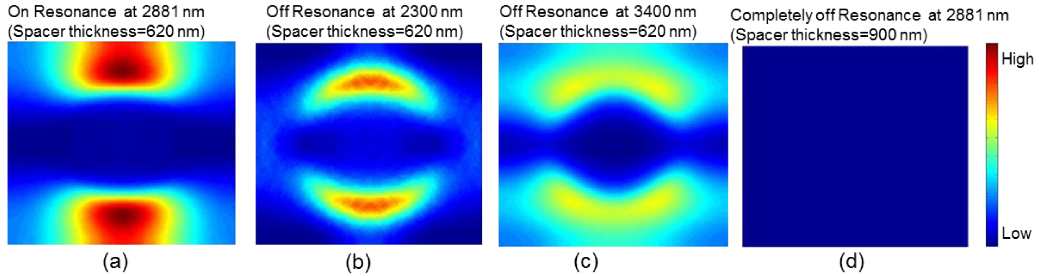
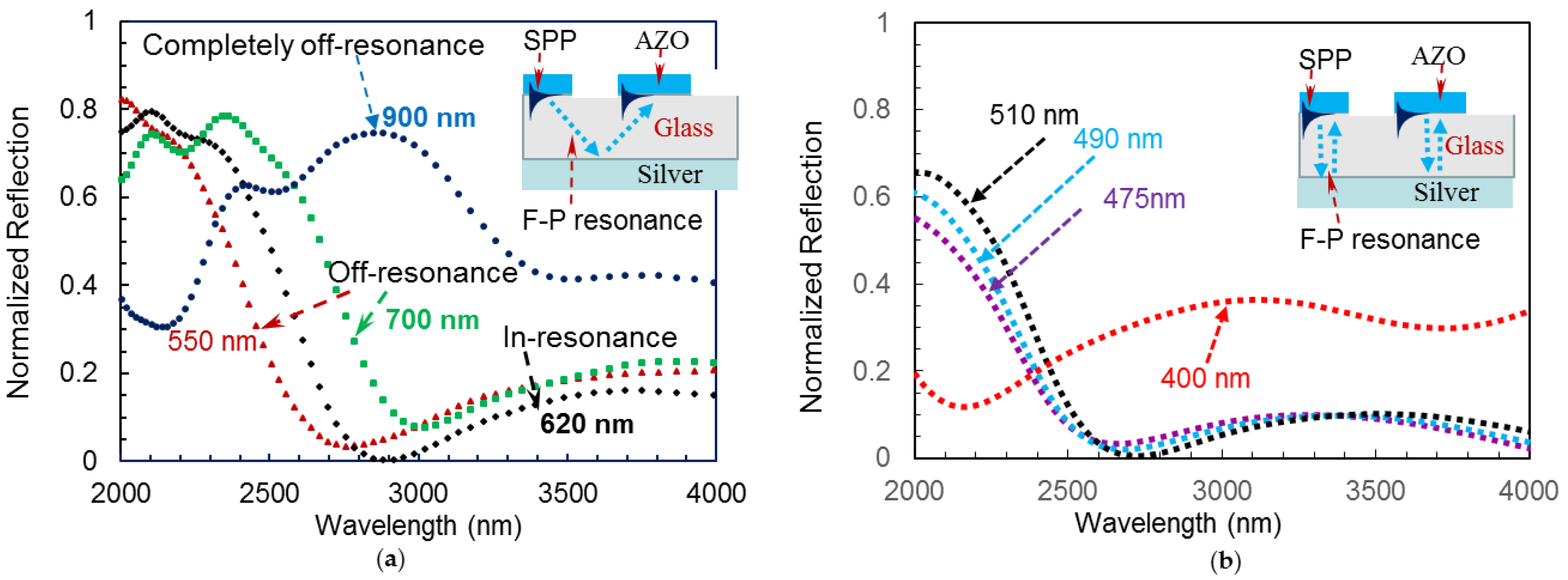
3.2. Coupling of SPP with F-P Resonance for TLA in Two Cavity Lengths

The mechanism of SPP coupling with F-P resonance is studied in this section. Figure 2a shows a simulated reflection spectrum from the square lattice hole array (without small holes) in a configuration of an AZO square lattice hole array/SiO2 spacer/silver/glass stack with SiO2 spacer thickness = 550, 620, 700 and 900 nm. The cross-section of the stack is shown as an insert in the figure. The thickness of AZO is 117 nm. With the spacer thickness = 900 nm, a broad reflection peak centered around 2881 nm was observed due to light coupling to the SPP in the (1,0) or (0,1) direction and being reflected by the silver film. This observed coupling can be understood by Equations (2)–(4), which are given below and denote the conditions for the coupling of the normal incident light into in-plane modes and for the formation of SPP standing wave, respectively:
Λ   n e f f = l 2 + m 2   λ
Λ   2 π λ   n e f f = p   π + φ
n e f f = ε A Z O ε s ε A Z O + ε s
where Λ is the lattice period, λ the wavelength, p the integer number, l and m diffraction indices, ϕ the phase shift due to the reflection, neff the effective refractive index as defined in Equation (4), and εAZO and εs the dielectric constants of the AZO and the spacer, respectively. Using Λ = 1528 nm (the period of square lattice fabricated [42]), p = 2 ( accumulates as SPP propagates through one period of lattices), ϕ = 0, (l,m) = (1,0) or (0,1) for diffraction direction, the calculated SPP resonance wavelength is at 2876 nm, very close to the reflection peak wavelength at 2881 nm.
As shown in the insert in Figure 2, F-P resonance can form between the AZO and the silver film. F-P resonance can be described in Equations (4) and (5) for the cavity length in Figure 2a,b, respectively:
F‑P   C a v i t y   L e n g t h = F P C L = 2 ( Λ 2 ) 2 + d 2
F‑P   C a v i t y   L e n g t h = F P C L = 2 d
where d is the thickness of the spacer. When d = 900 nm, SPP is completely off-resonant with the F-P resonance. When the thickness of the spacer is decreased from 900 nm to 700 nm, the reflection dip appeared due to the coupling of SPP and F-P resonance, but they are slightly off-resonant, as shown in Figure 2a. The same phenomenon happens for d = 550 nm. When d = 620 nm, zero reflection (thus TLA) happens around the wavelength of 2881 nm, due to the in-resonance coupling of SPP and F-P resonance with cavity path described by Equation (5) and shown in the inset of Figure 2a. From the spectra shown in Figure 2b, it is seen that the TLA condition is also met for a spacer thickness of 510 nm. For this spacer thickness, zero reflection happens around the wavelength of 2723 nm, due to the in-resonance coupling of SPP and the F-P resonance with cavity length described by Equation (6) and shown in the inset of Figure 2b. Slight variations away from the coupling resonance show slight variation from TLA, as seen by the reflection spectra with a spacer thickness of 475 nm and 490 nm. The spectra is completely off-resonant and no TLA is achieved when a spacer thickness value of 400 nm is used.
The formation of the F-P resonance needs to satisfy the following equation [46]:
F P C L   2 π λ   n s p a c e r = m   π + φ t o p + φ b o t t o m   ,   m = 1 , 2 , 3
where m is an integer number, ϕtop and ϕbottom are the additional phase shifts due to the reflection at the top and bottom surfaces of the spacer, respectively. For TLA to occur, SPP and F-P resonances must couple and simultaneously satisfy Equations (3) and (7). The phase shifts due to the top and bottom surfaces can be expressed in terms of the index of refractions and penetration depths, δ, into AZO and silver surfaces respectively: ϕtop = +(2   π /   λ ) ×   n A Z O × δAZO and ϕbottom = +(2   π / λ ) ×   n A g   × δAg. The penetration depths in the AZO or silver is given by:
  δ A z o , A g = λ S P P 2 π ε A z o , A g + ε d ( ε A z o , A g ) 2
where ε d and ε A z o , A g are the real permittivity of the dielectric spacer and conductive material (AZO or silver). Based on the Equations (3)–(8), the TLA wavelength in Figure 2a,b can be predicted to occur at 2828 and 2786 nm, respectively.

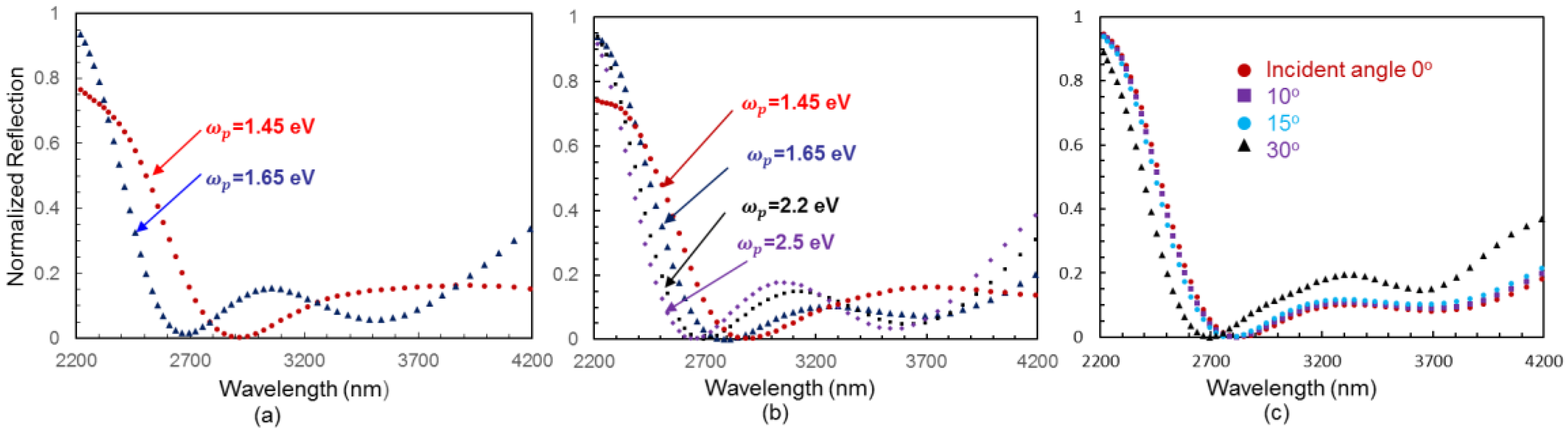
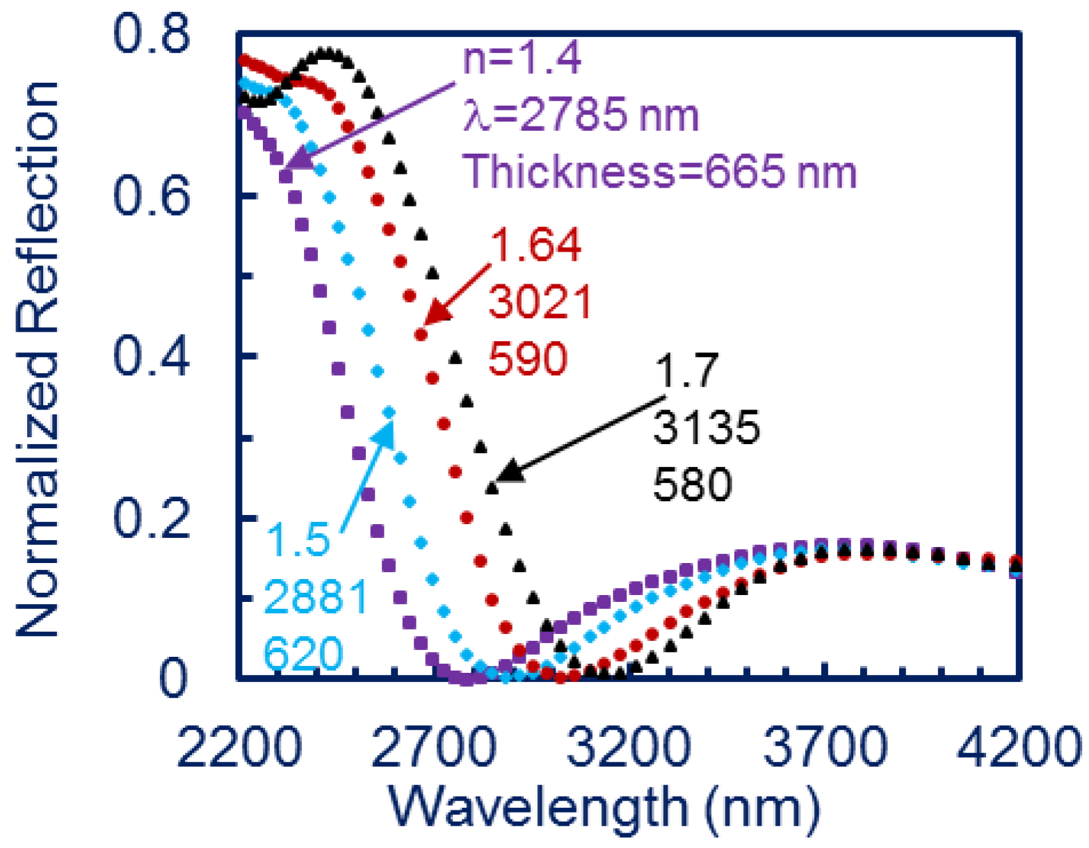
3.3. Refractive Index-Dependent SPP Coupling with F-P Resonance

The coupling mechanism in Equations (3)–(7) can be further tested. When the refractive index n of the spacer is changed, the effective refractive index in Equation (3) for SPP at the interface of the AZO and the spacer will be shifted, and SPP wavelength will also be different. In order to achieve the coupling of SPP and FP resonances, the thickness of the spacer needs to be varied to meet the condition imposed by Equation (7). The reflection spectra near 4000 nm wavelength for the in-resonance coupling in Figure 2a look completely different from those in Figure 2b, helping us determine whether to use the cavity length in Equation (5) (zig-zag cavity) or Equation (6). Figure 3 shows the simulated reflection spectra of the patterned AZO/ dielectric spacer/silver stack, where TLA occurs at wavelength, λ, of: 2785 nm, 2881 nm, 3021 nm and 3136 nm for different refractive indexes: n = 1.4, 1.5 (silica grass), 1.64 (Al2O3), and 1.7, respectively, for the zig-zag cavity. From the simulation, the thickness of spacer was found to be 665, 620, 590 and 580 nm for each spacer with a different refractive index n, as labeled in Figure 3.
Table 1 gives a cumulative summary of simulated TLA wavelengths from Figure 3, as well as calculated TLA wavelengths using Equation (7) for four refractive index values for the dielectric spacer. The penetration lengths into the AZO and silver used to determine the phase shift are given for each wavelength. From Table 1, the simulated TLA wavelength is very close to the calculated number using the F-P resonance, indicating the coupling of SPP and the F-P cavity.

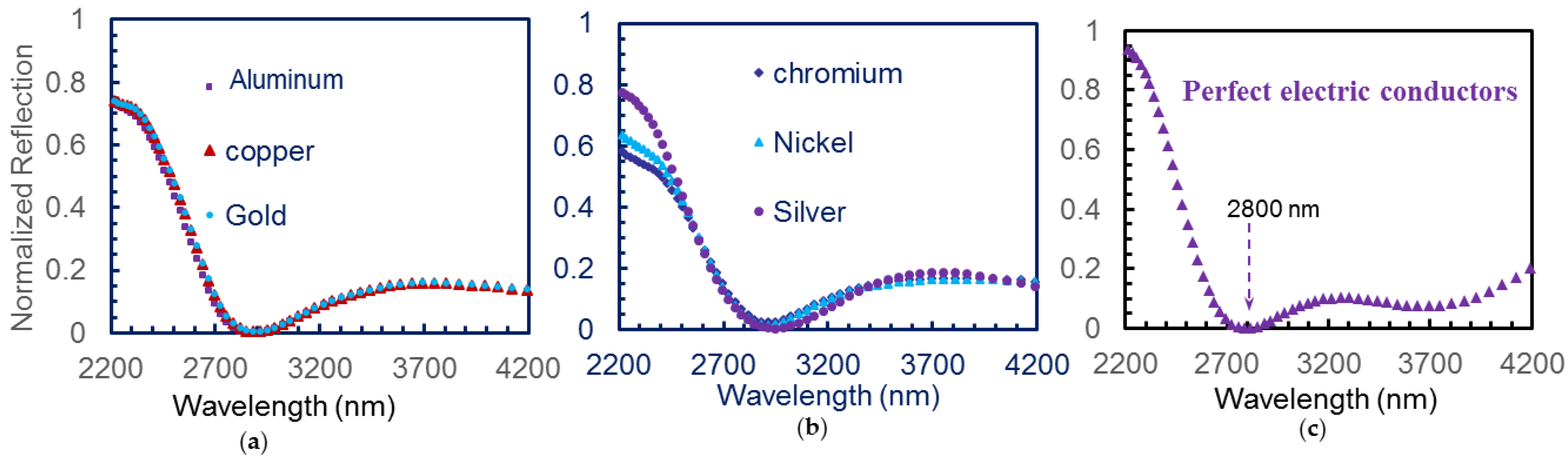
3.4. Effect of Metals on TLA

The metal choice can affect the TLA result because of the different losses that SPP experiences. Simulations in which the metal was varied in the AZO/SiO2 spacer/metal/glass stack structure are shown in Figure 4a,b. It can be seen that the TLA wavelength is not impacted with the use of gold, copper, aluminum, and is only minimally impacted when using nickel and chromium in comparison to using silver as the metal layer. This justifies the use of a more cost-effective metal without altering the TLA wavelength. Figure 4c shows the normalized reflection from the AZO/SiO2 spacer/perfect electric conductor stack structure. The wavelength of the TLA is at 2800 nm. The TLA location is moved to a lower wavelength than 2881 nm, as predicted by the theory.

3.5. Tunable TLA in AZO

One of the motivations for using AZO for the TLA structure is its potential application for tunable TLA, as studied in this section. The carrier concentration of AZO has been shown to be electrically tunable or thermally tunable via voltage biasing [39,40]. This change in carrier concentration is seen as a change in plasma frequency for AZO that effects the value of its permittivity and therefore the effective index of refraction, as described by Equation (9).
ω p = N e 2 m * ε 0
where e is the electron charge, m* the effective mass and ε0 the dielectric permittivity of vacuum.
Under heat, the plasma frequency of the whole layer of AZO can be changed [39]. Figure 5a shows the simulated reflection spectrum of the AZO/SiO2 spacer/silver/glass stack for two different values of plasma frequency in an AZO film with a thickness of 117 nm. The spacer thickness remained constant at 620 nm for each simulation. When the plasma frequency is 1.45 eV, the TLA wavelength is 2881 nm; but when the plasma frequency is changed to 1.65 eV, the dip wavelength blueshifts to 2694 nm.
Under negative voltage bias, the carrier concentration will continuously increase for the region close to the interface of the AZO/glass, as governed by Poisson’s equation [40]. In the simulation shown in Figure 5b, we assume the plasma frequency is changed to 1.65, 2.2 and 2.5 eV in 10 nm AZO close to the interface, while the plasma frequency is kept at 1.45 eV for the remaining part of the AZO layer with a thickness of 117 − 10 = 107 nm. The TLA is observed for all plasma frequencies and the TLA wavelength is blueshifted. However, the shifting is smaller than that in Figure 5a. These simulation results clearly indicate a tuning capability of AZO in TLA applications.

4. Discussion

In this study, SPP wavelength is determined by AZO and dielectric spacer properties but is not changed by the metallic layer, probably due to the lower loss in the infrared range for SPP to propagate along the AZO/dielectrics interface when compared to conventional metals. We did not observe coupling-induced absorption band splitting [35]. This might be due to the dominating F-P resonance in the dielectric spacer for the TLA [47].
We further studied the TLA for the oblique incidence. The plane wave source was used in the simulation. The simulated reflection spectra are shown in Figure 5c for incident angles of 0, 10, 15 and 30°. The TLA occurred for all incident angles in the figure. For 10 and 15°, the TLA wavelength barely changed from that at 0°, however, the wavelength for TLA location blue-shifted for the incident angle of 30°.
The on-resonance, off-resonance, and completely off-resonance couplings of the SPPs in AZO with the F-P resonances in the glass spacer layer were illustrated by the simulation spectra in Figure 2a. These couplings can be further verified by the E-field intensity distribution at a specific wavelength. At 2881 nm with a spacer thickness of 620 nm, as shown in in Figure 2a, TLA occurred due to the on-resonance coupling, and the E-field intensity was very strong as shown in Figure 6a. At 2300 and 3400 nm, away from the TLA wavelength as depicted in Figure 2a, E-field intensities became much weaker in Figure 6b,c than in Figure 6a, due to the off-resonance of SPP with F-P resonance. Even at 2881 nm with a spacer thickness = 900 nm, the E-field intensity was very weak, as shown in Figure 6d, due to the complete off-resonance of SPP with F-P resonance. These E-field intensity distributions, together with the simulated spectra, provide proofs of the coupling of SPP with F-P resonance.
Our studies also indicate potential AZO applications in post-fabrication tuning of plasmonic devices, such as an “on” and “off” switches if used for a detector and tuning lasing action in plasmonic lasers [48]. In a traditional laser such as an Ar ion laser, the cavity length can be adjusted to achieve the coupling of the F-P cavity mode with the active medium emission. For an AZO plasmonic device, the patterned AZO and spacer thickness is fixed after fabrication. Therefore, instead of changing the F-P cavity length, the AZO can be electrically tuned to couple the AZO SPP with the F-P cavity. Future research can be narrowed to work on a plasmonic system with stack structure of AZO/active lasing medium/metal for an interesting application in plasmonic lasing.

5. Conclusions

In summary, TLA in the infrared range has been simulated using AZO as a plasmonic material. TLA has been explained in terms of resonance coupling of the F-P mode with SPP through systemic simulations and theoretical calculations. Computed E-field intensity distributions, together with the simulated reflection spectra, have provided proofs of the coupling of SPP with F-P resonance. The electrical tuning capacity of an AZO plasmonic device has also been demonstrated in simulations.

Acknowledgments

This work was supported by research grants from the USA National Science Foundation under Grant Nos. CMMI-1266251 and ECCS-1407443.

Author Contributions

Y.L., J.C., U.P. and H.Z. conceived and designed simulations; D.G., M.A., S.H. and D.L. performed the simulations; Y.L., D.G. and M.A. analyzed the data; D.L. contributed parallel computation tools; Y.L. and D.G. wrote the paper. All authors read and comment on the manuscript.

Conflicts of Interest

The authors declare no conflict of interest. The founding sponsors had no role in the design of the study; in the collection, analyses, or interpretation of data; in the writing of the manuscript, and in the decision to publish the results.

References

  1. Chong, Y.D.; Cao, L.; Ge, H.; Stone, A.D. Coherent perfect absorbers: Time-reversed lasers. Phys. Rev. Lett. 2010, 105, 053901. [Google Scholar] [CrossRef] [PubMed]
  2. Zhang, B.; Hendrickson, J.; Guo, J. Multispectral near perfect metamaterial absorbers using spatially multiplexed plasmon resonance metal square structures. J. Opt. Soc. Am. B 2013, 30, 656–662. [Google Scholar] [CrossRef]
  3. Hendrickson, J.; Guo, J.B.; Zhang, W.B.; Soref, R. Wideband perfect light absorber at midwave infrared using multiplexed metal structures. Opt. Lett. 2012, 37, 371–373. [Google Scholar] [CrossRef] [PubMed]
  4. Fang, Z.; Zhen, Y.R.; Fan, L.; Zhu, X.; Nordlander, P. Tunable wide-angle plasmonic perfect absorber at visible frequencies. Phys. Rev. B 2012, 85, 245401. [Google Scholar] [CrossRef]
  5. Nielsen, M.G.; Pors, A.; Albrektsen, O.; Bozhevolnyi, S.I. Efficient absorption of visible radiation by gap plasmon resonators. Opt. Express 2012, 20, 13311–13319. [Google Scholar] [CrossRef] [PubMed]
  6. Kim, W.; Simpkins, B.S.; Long, J.P.; Zhang, B.; Hendrickson, J.; Guo, J. Localized and nonlocalized plasmon resonance enhanced light absorption in metal-insulator-metal nanostructures. J. Opt. Soc. Am. B 2015, 32, 1686–1692. [Google Scholar] [CrossRef]
  7. Sun, T.; Guo, C.F.; Cao, F.; Akinoglu, E.M.; Wang, Y.; Giersig, M.; Kempa, K. A broadband solar absorber with 12 nm thick ultrathin a-Si layer by using random metallic nanomeshes. Appl. Phys. Lett. 2014, 104, 251119. [Google Scholar] [CrossRef]
  8. Sturmberg, B.C.P.; Chong, T.K.; Choi, D.Y.; White, T.P.; Botten, L.C.; Dossou, K.B.; Poulton, C.G.; Catchpole, K.R.; McPhedran, R.C.; de Sterke, C.M. Total absorption of visible light in ultrathin weakly absorbing semiconductor gratings. Optica 2016, 3, 556–562. [Google Scholar] [CrossRef]
  9. Kats, M.A.; Blanchard, R.; Genevet, P.; Capasso, F. Nanometer optical coatings based on strong interference effects in highly absorbing media. Nat. Mater. 2013, 12, 20–24. [Google Scholar] [CrossRef] [PubMed]
  10. Kats, M.A.; Byrnes, S.J.; Blanchard, R.; Kolle, M.; Genevet, P.; Aizenberg, J.; Capasso, F. Enhancement of absorption and color contrast in ultra-thin highly absorbing optical coatings. Appl. Phys. Lett. 2013, 103, 101104. [Google Scholar] [CrossRef]
  11. Long, Y.; Su, R.; Wang, Q.; Shen, L.; Li, B.; Zheng, W. Deducing critical coupling condition to achieve perfect absorption for thin-film absorbers and identifying key characteristics of absorbing materials needed for perfect Absorption. Appl. Phys. Lett. 2014, 104, 091109. [Google Scholar] [CrossRef]
  12. Ding, B.; Qiu, M.; Blaikie, R.J. Manipulating light absorption in dye-doped dielectric films on reflecting surfaces. Opt. Express 2014, 22, 25965–25975. [Google Scholar] [CrossRef] [PubMed]
  13. Song, H.; Guo, L.; Liu, Z.; Liu, K.; Zeng, X.; Ji., D.; Zhang, N.; Hu, H.; Jiang, S.; Gan, Q. Nanocavity enhancement for ultra-thin film optical absorber. Adv. Mater. 2014, 26, 2737–2743. [Google Scholar] [CrossRef] [PubMed]
  14. Schlich, F.F.; Spolenak, R. Strong interference in ultrathin semiconducting layers on a wide variety of substrate materials. Appl. Phys. Lett. 2013, 103, 213112. [Google Scholar] [CrossRef]
  15. Li, Z.; Butun, S.; Aydin, K. Large-area lithography-free super absorbers and color filters at visible frequencies using ultrathin metallic films. ACS Photonics 2015, 2, 183–188. [Google Scholar] [CrossRef]
  16. Li, Z.; Palacios, E.; Butun, S.; Kocer, H.; Aydin, K. Omnidirectional broadband light absorption using large- area ultrathin lossy metallic film coatings. Sci. Rep. 2015, 5, 15137. [Google Scholar] [CrossRef] [PubMed]
  17. Wang, Z.; Luk, T.S.; Tan, Y.; Ji, D.; Zhou, M.; Gan, Q.; Yu, Z. Tunneling-enabled spectrally selective thermal emitter based on flat metallic films. Appl. Phys. Lett. 2015, 106, 101104. [Google Scholar] [CrossRef]
  18. Lee, K.T.; Seo, S.; Lee, J.Y.; Guo, L.J. Strong resonance effect in a lossy medium-based optical cavity for angle robust spectrum filters. Adv. Mater. 2014, 26, 6324–6328. [Google Scholar] [CrossRef] [PubMed]
  19. Streyer, W.; Law, S.; Rooney, G.; Jacobs, T.; Wasserman, D. Strong absorption and selective emission from engineered metals with dielectric coatings. Opt. Express 2013, 21, 9113–9122. [Google Scholar] [CrossRef] [PubMed]
  20. Mirshafieyan, S.S.; Guo, J. Silicon colors: Spectral selective perfect light absorption in single layer silicon films on aluminum surface and its thermal tunability. Opt. Express 2014, 22, 31545–31554. [Google Scholar] [CrossRef] [PubMed]
  21. Lee, K.T.; Ji, C.; Guo, L.J. Wide-angle, polarization-independent ultrathin broadband visible absorbers. Appl. Phys. Lett. 2016, 108, 031107. [Google Scholar] [CrossRef]
  22. Kocer, H.; Butun, S.; Li, Z.; Aydin, K. Reduced near-infrared absorption using ultra-thin lossy metals in Fabry-Perot cavities. Sci. Rep. 2015, 5, 8157. [Google Scholar] [CrossRef] [PubMed]
  23. Mirshafieyan, S.S.; Luk, T.S.; Guo, J. Zeroth order Fabry-Perot resonance enabled ultra-thin perfect light absorber using percolation aluminum and silicon nanofilms. Opt. Mater. Express 2016, 6, 1032–1042. [Google Scholar] [CrossRef]
  24. Hosseini, P.; Wright, C.D.; Bhaskaran, H. An optoelectronic framework enabled by low-dimensional phase- change films. Nature 2014, 511, 206–211. [Google Scholar] [CrossRef] [PubMed]
  25. Schlich, F.F.; Zalden, P.; Lindenberg, A.M.; Spolenak, R. Color switching with enhanced optical contrast in ultrathin phase-change materials and semiconductors induced by femtosecond laser pulses. ACS Photonics 2015, 2, 178–182. [Google Scholar] [CrossRef]
  26. Cleary, J.W.; Soref, R.; Hendrickson, J.R. Long-wave infrared tunable thin-film perfect absorber utilizing highly doped silicon-on-sapphire. Opt. Express 2013, 21, 19363–19374. [Google Scholar] [CrossRef] [PubMed]
  27. Liang, J.; Hou, L.; Li, J. Frequency tunable perfect absorber in visible and near-infrared regimes based on VO2 phase transition using planar layered thin films. J. Opt. Soc. Am. 2016, 33, 1075–1080. [Google Scholar] [CrossRef]
  28. Kats, M.A.; Sharma, D.; Lin, J.; Genevet, P.; Blanchard, R.; Yang, Z.; Qazilbash, M.M.; Basov, D.N.; Ramanathan, S.; Capasso, F. Ultra-thin perfect absorber employing a tunable phase change material. Appl. Phys. Lett. 2012, 101, 221101. [Google Scholar] [CrossRef]
  29. Aydin, K.; Ferry, E.V.; Briggs, M.R.; Atwater, H.A. Broadband polarization-independent resonant light absorption using ultrathin plasmonic super absorbers. Nat. Commun. 2011, 2, 517. [Google Scholar] [CrossRef] [PubMed]
  30. Luk, T.S.; Fofang, N.T.; Cruz-Campa, J.L.; Frank, I.; Campione, S. Surface plasmon polariton enhanced ultrathin nano-structured CdTe solar cell. Opt. Express 2014, 22, A1372–A1379. [Google Scholar] [CrossRef] [PubMed]
  31. Chen, H. Interference theory of metamaterial perfect absorbers. Opt. Express 2012, 20, 7165–7172. [Google Scholar] [CrossRef] [PubMed]
  32. Yang, Y.; Kamaraju, N.; Campione, S.; Liu, S.; Reno, J.L.; Sinclair, M.B.; Prasankumar, R.P.; Brener, I. Transient GaAs Plasmonic Metasurfaces at Terahertz Frequencies. ACS Photonics 2017, 4, 15–21. [Google Scholar] [CrossRef]
  33. Campione, S.; Kim, I.; de Ceglia, D.; Keeler, G.A.; Luk, T.S. Experimental verification of epsilon-near-zero plasmon polariton modes in degenerately doped semiconductor nanolayers. Opt. Express 2016, 24, 18782–18789. [Google Scholar] [CrossRef] [PubMed]
  34. Luk, T.S.; Campione, S.; Kim, I.; Feng, S.; Jun, Y.C.; Liu, S.; Wright, J.B.; Brener, I.; Catrysse, P.B.; Fan, S.; et al. Directional perfect absorption using deep subwavelength low-permittivity films. Phys. Rev. B 2014, 90, 085411. [Google Scholar] [CrossRef]
  35. Yoon, J.; Zhou, M.; Badsha, M.A.; Kim, T.Y.; Jun, Y.C.; Hwangbo, C.K. Broadband Epsilon-Near-Zero Perfect Absorption in the Near-Infrared. Sci. Rep. 2015, 5, 12788. [Google Scholar] [CrossRef] [PubMed]
  36. Kim, T.Y.; Badsha, M.A.; Yoon, J.; Lee, S.Y.; Jun, Y.C.; Hwangbo, C.K. General Strategy for Broadband Coherent Perfect Absorption and Multi-wavelength All-optical Switching Based on Epsilon-Near-Zero Multilayer Films. Sci. Rep. 2016, 6, 22941. [Google Scholar] [CrossRef] [PubMed]
  37. Zhu, C.; Li, J.; Yang, Y.; Huang, J.; Lu, Y.; Zhao, X.; Tan, R.; Dai, N.; Song, W. SiO2/bi-layer GZO/Ag structures for near-infrared broadband wide-angle perfect absorption. J. Phys. D: Appl. Phys. 2016, 49, 425106. [Google Scholar] [CrossRef]
  38. Cleary, J.W.; Nader, N.; Leedy, K.D.; Soref, R. Tunable short-to mid-infrared perfectly absorbing thin films utilizing conductive zinc oxide on metal. Opt. Mater. Express 2015, 5, 1898–1909. [Google Scholar] [CrossRef]
  39. Pradhan, A.K.; Mundle, R.M.; Santiago, K.; Skuza, J.R.; Xiao, B.; Song, K.D.; Bahoura, M.; Cheaito, R.; Hopkins, P.E. Extreme tunability in aluminum doped Zinc Oxide plasmonic materials for near-infrared applications. Sci. Rep. 2014, 4, 6415. [Google Scholar] [CrossRef] [PubMed]
  40. George, D.; Li, L.; Lowell, D.; Ding, J.; Cui, J.; Zhang, H.; Philipose, U.; Lin, Y. Electrically tunable diffraction efficiency from gratings in Al-doped ZnO. Appl. Phys. Lett. 2017, 110, 071110. [Google Scholar] [CrossRef]
  41. Kinsey, N.; DeVault, C.; Kim, J.; Ferrera, M.; Shalaev, V.M.; Boltasseva, A. Epsilon-near-zero Al-doped ZnO for ultrafast switching at telecom wavelengths. Optica 2015, 2, 616–622. [Google Scholar] [CrossRef]
  42. George, D.; Li, L.; Jiang, Y.; Lowell, D.; Mao, M.; Hassan, S.; Ding, J.; Cui, J.; Zhang, H.; Philipose, U.; et al. Localized Surface Plasmon Polariton Resonance in Holographically Structured Al-doped ZnO. J. Appl. Phys. 2016, 120, 043109. [Google Scholar] [CrossRef]
  43. Oskooi, A.F.; Roundy, D.; Ibanescu, M.; Bermel, P.; Joannopoulos, J.D.; Johnson, S. MEEP: A flexible free-software package for electromagnetic simulations by the FDTD method. Compu. Phys. Commun. 2010, 181, 687–702. [Google Scholar] [CrossRef]
  44. Wu, L.; Bai, P.; Li, E.P. Designing surface plasmon resonance of subwavelength hole arrays by studying absorption. J. Opt. Soc. Am. B 2012, 29, 521. [Google Scholar] [CrossRef]
  45. Rakic, A.D.; Djurisic, A.B.; Elazar, J.M.; Majewski, M.L. Optical properties of metallic films for vertical-cavity optoelectronic devices. Appl. Opt. 1998, 37, 5271–5283. [Google Scholar] [CrossRef] [PubMed]
  46. Cui, Y.; He, Y.; Jin, Y.; Ding, F.; Yang, L.; Ye, Y.; Zhong, S.; Lin, Y.; He, S. Plasmonic and Metamaterial Structures as Electromagnetic Absorbers. Laser Photonics Rev. 2014, 8, 495–520. [Google Scholar] [CrossRef]
  47. Park, J.; Kang, J.; Kim, S.J.; Liu, X.; Brongersma, M.K. Dynamic Reflection Phase and Polarization Control in Metasurfaces. Nano Lett. 2017, 17, 407–413. [Google Scholar] [CrossRef] [PubMed]
  48. Wu, C.; Khanal, S.; Reno, J.; Kumar, S. Terahertz plasmonic laser radiating in an ultra-narrow beam. Optica 2016, 3, 734–740. [Google Scholar] [CrossRef]
Figure 1. Simulations of transmission spectrum through super-lattice hole array in Al-doped ZnO (AZO) for light polarization in the (1,1) direction (a) and in the (1,0) direction (b). A smaller hole is introduced in the unit cell of the bigger hole array, as shown in insert indicated by dashed red squares. The colored numbers near the solid black arrow indicate the diameter (in nm) of the smaller holes used for each simulation respectively; (c) Computed E-field intensities at two wavelengths of 2881 nm (c1) and 3400 nm (c2) with a polarization in (1,0); (d) Computed E-field intensity in the dual hole structure with a polarization in (1,0).
Photonics 04 00035 g001
Figure 2. (a) Simulated reflection spectra from a stack of AZO hole arrays/spacer/silver for a spacer thickness of 550, 620, 700 and 900 nm. Total light absorption (TLA) is achieved when a surface plasmon polariton (SPP) couples with the F-P resonance in zig-zag fashion, as shown in the inset; (b) Simulated reflection spectra for a spacer thickness of 475, 490, and 510 nm. The coupling of SPP with F-P resonance occurs at a shorter cavity length than in the case in (a), as shown in the insert. When the thickness is decreased to 400 nm, off-resonance appears.
Photonics 04 00035 g002
Figure 3. Simulations of the reflection spectrum of patterned AZO thin film separated from a thin film of silver by a spacer with an index of refraction n = 1.4 (purple), 1.5 (blue), 1.64 (red) and 1.7 (black). Total light absorption occurs at wavelength λ when the thickness of the spacer material meets the F-P condition for different indexes of refraction.
Photonics 04 00035 g003
Figure 4. Simulations of the reflection spectrum of the patterned AZO, glass spacer and metal film stacks for a group of metals of aluminum, copper and gold (a); a group of metals of chromium, nickel and silver (b); and when the metal is replaced by perfect electric conductors (c).
Photonics 04 00035 g004
Figure 5. (a) Simulations of the reflection spectrum of a patterned AZO/glass spacer/metal thin film stack for a plasma frequency ωp of 1.65 eV (blue line) and 1.45 eV (red line) for the AZO; (b) Simulations of the reflection spectrum from patterned AZO/glass spacer/metal when the plasma frequency is changed to 1.65, 2.2 and 2.5 eV for 10 nm AZO near the AZO/glass interface while the plasma frequency is kept at 1.45 eV for the remaining part of the AZO layer with a thickness of 117 − 10 = 107 nm; (c) Simulations of the reflection spectrum with the plasma frequency of 1.45 eV, but with different incident angles of 0, 10, 15, and 30°.
Photonics 04 00035 g005
Figure 6. Computed E-field intensity distribution inside the spacer layer in the AZO hole array/spacer/silver stack: (a) Mode profile at 2881 nm for the on-resonance case with the spacer thickness = 620 nm; (b) Mode profile for off-resonance cases at 2300 nm and (c) at 3400 nm with the spacer thickness = 620 nm; (d) Mode profile at 2881 nm for the completely off-resonance case with the spacer thickness = 900 nm.
Photonics 04 00035 g006
Table 1. Optical properties of multi-layer structures, SPP wavelength and F-P wavelength.
Refractive Index of Spacer1.41.51.641.7
Simulated dip wavelength (nm)27852881 1, 2723 230213135
Penetration in AZO (nm)14514,711,432142141
Penetration in silver (nm)2424 1, 24 22424
Calculated F-P wavelength (nm)27192828 1, 2786 230373125
Spacer thickness (nm)665620 1, 510 2590580
1 F-P cavity (zig-zag) length from Figure 1a; 2 F-P cavity length from Figure 1b.

