Site-Controlled Quantum Emitters in Dilute Nitrides and their Integration in Photonic Crystal Cavities
by
 , , ,
, , ,
Giorgio Pettinari
1,* ,
,
Marco Felici
2,
Francesco Biccari
3,
Mario Capizzi
2 and
Antonio Polimeni
2 
1
National Research Council, Institute for Photonics and Nanotechnologies (IFN-CNR), Via Cineto Romano 42, I-00156 Rome, Italy
2
Dipartimento di Fisica, Sapienza Università di Roma, P.le A. Moro 5, I-00185 Roma, Italy
3
Department of Physics and Astronomy, University of Florence, via Sansone 1, I-50019 Sesto Fiorentino (FI), Italy
*
Author to whom correspondence should be addressed.
Photonics 2018, 5(2), 10; https://doi.org/10.3390/photonics5020010
Submission received: 9 April 2018
/
Revised: 4 May 2018
/
Accepted: 11 May 2018
/
Published: 15 May 2018
Abstract
:We review an innovative approach for the fabrication of site-controlled quantum emitters (i.e., single-photon emitting quantum dots) based on the spatially selective incorporation and/or removal of hydrogen in dilute nitride semiconductors (e.g., GaAsN). In such systems, the formation of stable N-H complexes removes the effects that nitrogen has on the alloy properties, thus enabling the in-plane engineering of the band bap energy of the system. Both a lithographic approach and/or a near-field optical illumination—coupled to the ultra-sharp diffusion profile of H in dilute nitrides—allow us to control the hydrogen implantation and/or removal on a nanometer scale. This, eventually, makes it possible to fabricate site-controlled quantum dots that are able to emit single photons on demand. The strategy for a deterministic spatial and spectral coupling of such quantum emitters with photonic crystal cavities is also presented.
1. Introduction
Owing to their ability to act as sources of non-classical light in the solid state, semiconductor quantum dots (QDs) might serve as the main building blocks of several potentially ground-breaking devices, thus enabling the first practical implementation of quantum information technology (e.g., quantum computation, quantum teleportation, and quantum cryptography) [1,2]. The possibility to tune their emission energy and to have a narrow luminescence linewidth has, indeed, already made QDs predominant in several different technological fields, from solid-state lighting (e.g., LED and lasers) to biology, from photovoltaic to sensor devices [3,4]. In this scenario, a fine control on the position, size, density, and confinement potential of QDs is highly desirable—when not strictly necessary. Therefore, the development of technologies able to provide site-controlled quantum emitters based on QDs is strongly pursued by industry and research groups. In particular, one of the most difficult requests to fulfill is the fine control on the QD position, especially for QDs obtained by the most widely used standard growth methods (i.e., Stranski-Krastanow and droplet epitaxy), which are intrinsically random processes [5,6]. In the last two decades, several methods have been developed to control the QD nucleation position [5,7], in order to integrate site-controlled QDs in photonic structures, i.e., a fundamental step towards the practical implementation of quantum devices. The most successful approach is represented perhaps by the self-limited growth of QDs into inverted pyramidal recesses etched in a GaAs substrate [8,9,10], which gives a position accuracy of about 50 nm [11]. Preferential sites for QD nucleation can also be defined by growing InP pyramids by selective-area epitaxy [12,13,14] or by patterning the substrate with nano-hole arrays [15,16,17,18,19], with a spatial accuracy better than 50 nm and 80 nm, respectively, and a possible integration with photonic devices. The main characteristics of those site-controlled QD fabrication techniques are reported in Table 1. Other approaches to the fabrication of site-controlled QDs include the self-organization of individual InAs QDs by scanning tunneling probe-assisted nanolithography [20], the “vicinal substrate” approach [21], the nucleation of InAs QDs on strain modulated buffer layers grown on submicron mesa arrays [22], and quantum-well etching [23]. All the techniques not included in Table 1, however, are either incompatible with the integration with optical micro-cavities, since they are characterized by an insufficient spatial accuracy, or not really scalable, and therefore unsuitable for future applications in quantum information technology.
Different lithographic strategies have also been developed to deterministically fabricate a photonic device around a post-selected, self-assembled QD [2,24,25,26]. These techniques, which can reach a spatial accuracy up to 50 nm, avoid in principle the need for site-controlled QDs. However, they are intrinsically not scalable—and therefore not suitable for the mass production—although strategies for increasing the number of implemented devices within a given processing time are being investigated [27].
In this review, we report on an innovative approach we developed for the fabrication of site-controlled QDs, which are able to emit down to the single-photon regime. Our approach is based on the spatially selective incorporation and/or removal of hydrogen in dilute nitride semiconductors (e.g., GaAsN) [28,29,30]. Our fabrication strategy, at variance with the approaches proposed so far in the literature that rely on complex growth procedures often followed by cumbersome processing steps, starts from standard dilute-nitride quantum well samples and acts at a post-growth level. Therefore, it is easy, cost-effective, and extremely versatile. Moreover, it is scalable and guarantees an easy integration of the fabricated, site-controlled quantum emitters with photonic crystal cavities. Finally, it allows a spatial and spectral accuracy comparable to—or even better than—those obtained with other, more established techniques (see Table 1). It should be noted that the proposed approach can also be applied to different dilute nitrides, such as GaAsN, GaPN, and InGaAsN, in which N-effects have been shown to be neutralized by hydrogen [31].
In the following, we first briefly introduce the physical process on which the proposed fabrication processes rely, i.e., the peculiar effects of hydrogen in dilute nitrides (Section 2). Then (Section 3), we present fabrication approaches based either on spatially selective hydrogen incorporation (Section 3.1) or on spatially selective hydrogen removal (Section 3.2), both approaches having been successfully applied to the fabrication of site-controlled, single-photon emitters. Finally (Section 4), our strategy for the deterministic spatial and spectral coupling of such quantum emitters with photonic crystal cavities is presented.
2. Hydrogen Effects in Dilute Nitrides
Dilute nitride semiconductors are III-V alloys in which small percentages of nitrogen atoms (~1%) replace the group-V elements and present many interesting and counterintuitive physical properties [32,33,34]. Despite the small amount of substituted atoms, N perturbs dramatically the electronic properties of the host crystal, leading to a counterintuitive and large decrease in the bandgap energy [35,36,37,38], a non-monotonic variation of the electron effective mass [39,40,41] and gyromagnetic factor [42,43,44], and a softened response to external perturbations, such as hydrostatic pressure [45,46,47] and temperature [48,49]. All these effects are ascribable to the formation of N-related localized states that are resonant with (or close to) the extended states of the conduction band (CB) of the host lattice [50]. The quantum interaction between these two sets of states leads to a distortion of the energy-wavevector dispersion curve and to the formation of a fully-developed energy gap in the CB of the host crystal, which is eventually responsible for the drastic reduction in the bandgap energy with increasing N concentration.
2.1. Hydrogen-Induced Band-Gap Tuning
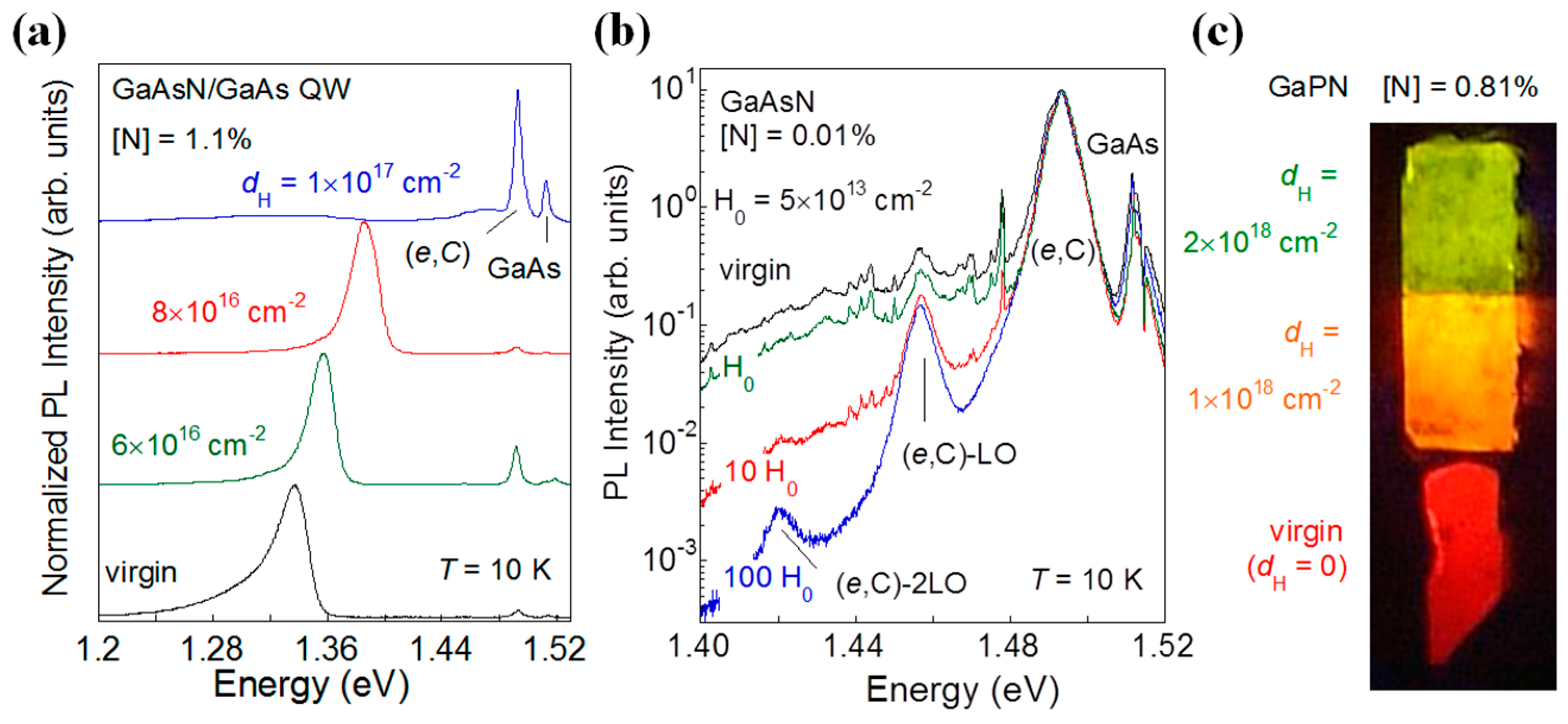
The change in the properties of dilute nitrides after irradiation with atomic hydrogen is an additional, unique, and exciting feature of these materials. Hydrogen, which is present in most growth and post-growth steps of semiconductor processing, affects the optical and electrical properties of the materials it enters in more ways than one. In particular, it is well-known that H often passivates shallow and deep defects, thus largely modifying the conductivity of several semiconductors [51,52]. Recently, it has also been shown that H neutralizes the native p-type conductivity in GaAsBi [53], opens the gap in InN and in In-rich InGaN [54], and increases the electron concentration in InAsN [55]. As for dilute nitrides, remarkably, H neutralizes N-induced effects in various III-V compounds and alloys [31]. It was discovered, indeed, that hydrogen incorporation modifies the band-gap energy (Eg) of GaAsN [56,57,58], InGaAsN [59,60], and GaPN [61], leading to a recovery of the Eg value of the N-free host. The hydrogen-induced band-gap tuning process is illustrated in Figure 1 for the GaAsN and GaPN cases. Although these materials emit in very different wavelength ranges, they share quite similar electronic properties. For the GaAsN case, we show two very different N concentrations irradiated at different H doses. Figure 1a refers to a GaAsN/GaAs quantum well (QW) with width L = 6 nm and nitrogen concentration [N] = 1.1%. Clearly, with increasing hydrogen dose (dH) the photoluminescence (PL) peak (due to exciton recombination in the well) blueshifts, until it reaches the energy position expected for the N-free material. Figure 1b displays, instead, the PL spectra of a GaAsN epilayer (t = 110 nm) in the very dilute concentration limit, i.e., [N] < 0.1%. In this limit, the band-gap energy is slightly affected by N incorporation, while the crystal emission is characterized by a series of very sharp lines (linewidth ~0.5 meV) due to the radiative recombination of excitons localized on N complexes (such as N pairs, triplets, or higher-order clusters); see topmost spectrum. These lines are superimposed on a broad band, also related to N alloying. Hydrogenation leads to a progressive and finally complete quenching of the N-related lines, as well as of the broad underlying band [62]. As regards the GaPN case, which emits in the visible range of the electromagnetic spectrum, the tuning of the band gap energy by H appears evident even to a naked-eye inspection of the sample. Figure 1c shows the photographic image of two GaPN epilayers (t = 250 nm, [N] = 0.81%), acquired at T = 10 K and under laser excitation. The epilayer in the upper part of the picture was treated with two different dH along its length, while the one in the lower part (shown as a reference) was left untreated. The emission clearly shifts from red to green by increasing the H dose, nicely confirming the possibility to tune the emission wavelength (i.e., the energy gap) of the material by H irradiation.
As extensively investigated in the case of GaAsN, the tuning of the band-gap energy is accompanied by a H-induced tuning of the electron effective mass [39] and gyromagnetic factor [42], which clearly indicates that the entire band structure of the system is profoundly affected by H, and that the attainment of a fine control on H incorporation would provide us with the means to finely tune the electronic properties of the alloy. Furthermore, even the structural characteristics of H-irradiated GaAsN undergo major modifications: A reversal of strain from tensile to compressive and an effective re-establishment of local ordering were indeed reported [63].
In the next paragraph, we describe briefly the microscopic structure of the N–H complexes responsible for the band-gap reopening, how these complexes distribute in the crystal, and how they can be dissociated to make the H effect reversible.
2.2. Nitrogen-Hydrogen Complex Formation and Spatial Distribution
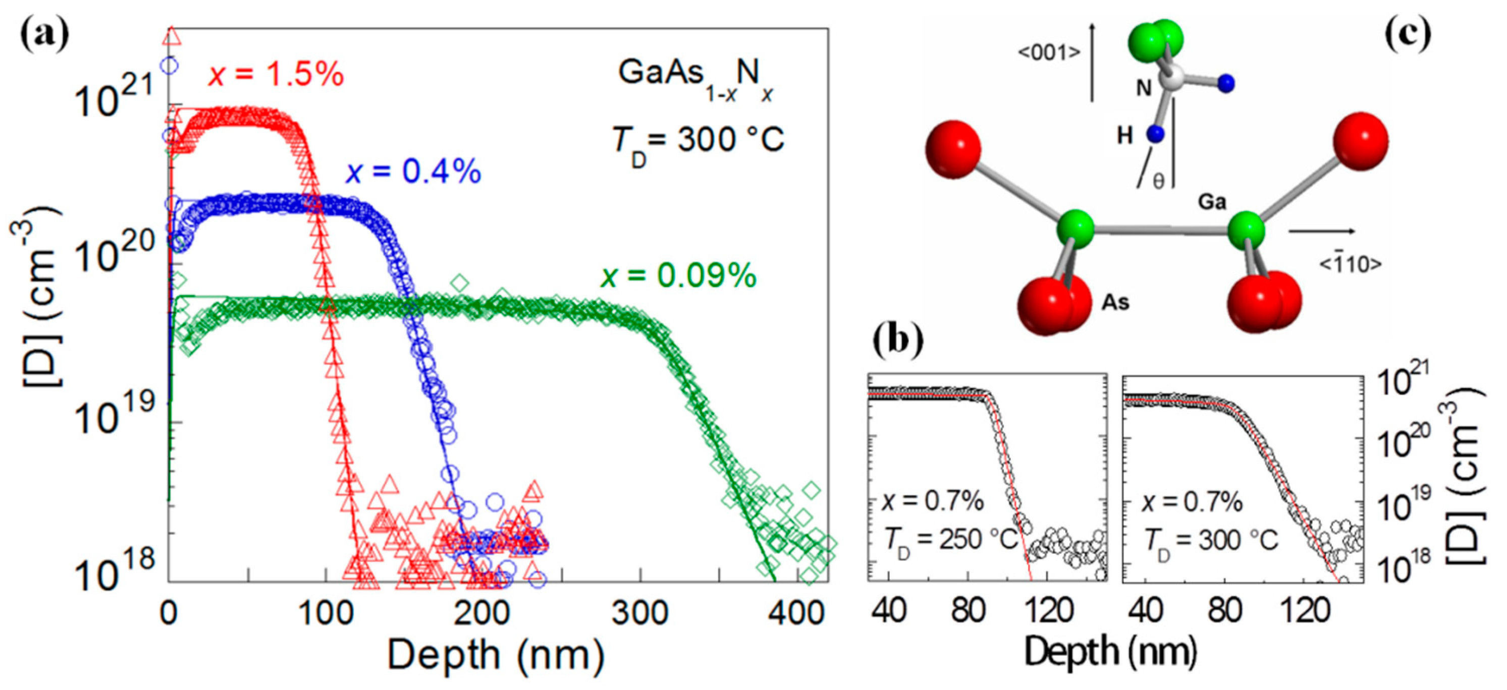
Infrared absorption studies of GaAsN epilayers treated with both hydrogen and deuterium (D) revealed that the complex causing the passivation of the electronic activity of N has the canted C1h geometry shown in Figure 2c [64]. Additionally, this C1h complex also accounts for the X-ray absorption near-edge structure of N atoms detected in hydrogenated GaAsN [65]. To date, it is considered the most likely complex responsible for nitrogen passivation [66,67,68].
A careful investigation of hydrogen diffusion (actually, of deuterium, customarily used in order to observe isotpe effects and to increase the measurement sensitivity) in GaAsN has revealed that a very sharp D profile is achieved in proper samples and under suitable conditions. Specifically, N concentrations greater than 0.5% and deuteration temperatures (TD) lower than 250 °C result in markedly steep D profiles, in which the concentration of electronically active (namely, not passivated) N atoms drops by a factor of ten in less than 5 nm [69]. This is shown in Figure 2, which displays deuterium concentration profiles (symbols) for different nitrogen concentrations (panel a) and TD (panel b), as derived in GaAsN by secondary-ion-mass spectrometry (SIMS) measurements. Simulations (solid lines) that accurately reproduce the data have been obtained by solving a system of differential equations, describing the time evolution of the concentration of free N and D atoms and of the different N–D complexes forming and dissociating in the lattice during the deuteration process [69]. A key point accounting for the D profile is the multiple trapping character of D diffusion, in which passivating D atoms do not proceed further into the crystal until stable C1h defects stop forming.
2.3. Reversibility of the Hydrogen Effects
Before moving further to the quantum-emitter fabrication approaches, we review the different methodologies employed to dissociate the N–H complexes responsible for the electronic passivation of N activity in dilute nitrides. This is an issue of high relevance, since it addresses both the stability of the effects induced by hydrogen and the possibility to spatially modulate these effects after N–H complexes have been formed. Three different approaches are possible for N–H complex dissociation, namely, thermal-, electron-, and photon-induced dissociation. Here we focus on the photon-induced dissociation approach, which is at the basis of the QD direct-writing fabrication technique by near-field illumination that we will present later (see Section 3.2). Details on the other two approaches can be found, respectively, in Refs. [57,60,70,71].
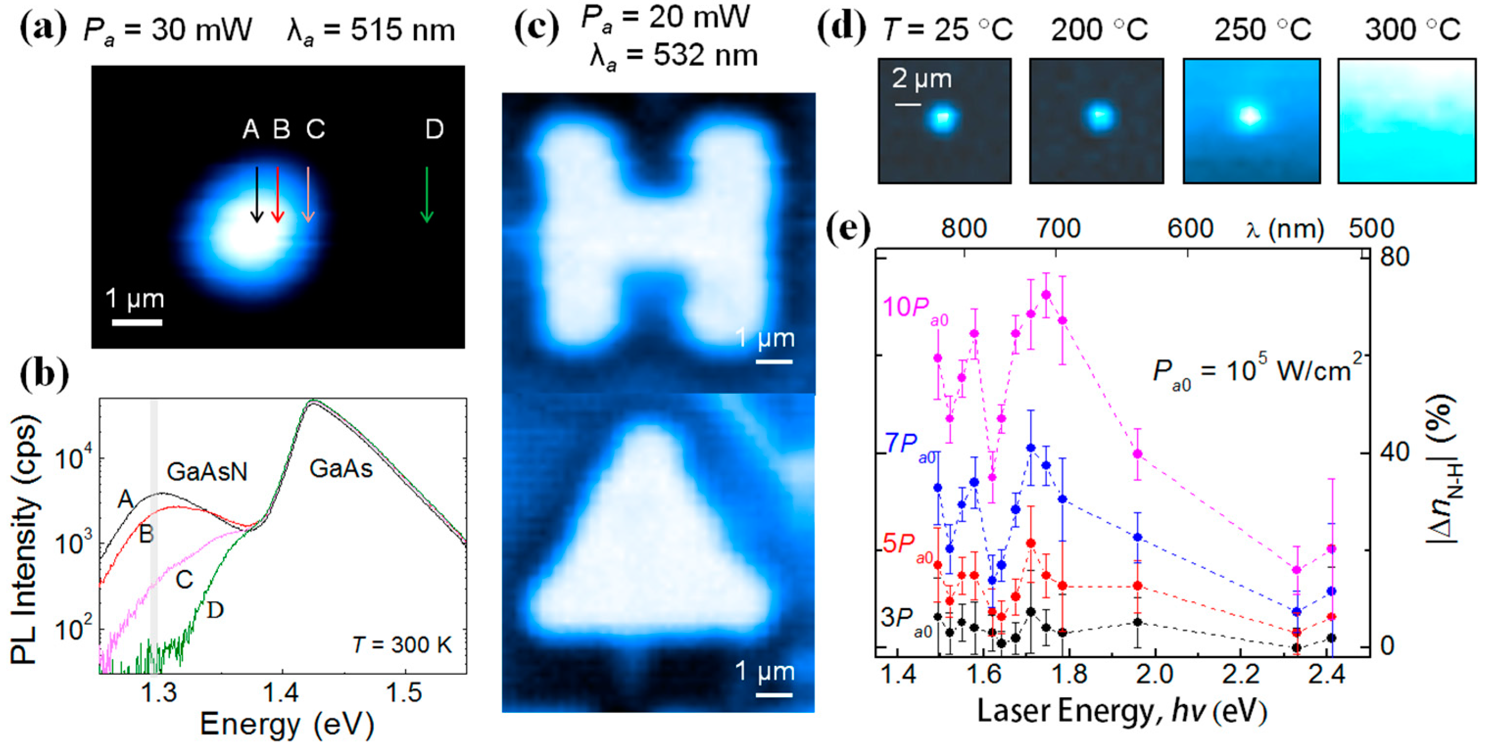
The combination of hydrogenation and photon-induced dissociation provides a successful, versatile tool for the tuning and spatial control of the optical properties of dilute nitride alloys. Indeed, it has been shown that the N–H complex responsible for the passivation of N is dissociated, by means of a purely photonic effect, upon exposing the sample to a focused laser beam [72]. Figure 3a,b shows the room temperature (T = 300 K) micro-photoluminescence (μPL) map and spectra of a hydrogenated GaAsN sample (dH = 6 × 1016 cm−2, [N] = 0.9%) after exposure for a time ta = 15 s to a focused laser beam (of diameter d ~ 1 μm and wavelength λ = 515 nm) with laser power Pa = 30 mW. The μPL spectra were acquired at low excitation power (~Pa/20) inside and outside the laser-exposed spot. It can be seen that the QW PL emission peaks at increasingly low energies when moving from outside to inside the laser exposed spot; see the μPL spectra at positions A, B, C, and D in Figure 3b. The μPL map in the spectral range of the QW emission shows a light-emitting region with an approximately Gaussian intensity distribution and a full-width at half-maximum (FWHM) of ~0.95 μm, which corresponds closely to the laser spot diameter. By keeping the laser power low enough (Pa ≤ 40 mW), no surface damage is produced by the laser treatment [72]. Moreover, at variance with thermal annealing treatments that affect the whole sample [57,60,70], laser treatment is limited only by the diffraction of the laser light, thus allowing a control of the optical properties of dilute nitrides on a micrometer scale. The high versatility of this photonic approach, as regards both the size and shape of the treated region, is exemplified by the micrometer-sized emitting areas, respectively shaped as an “H” and as a triangle, obtained by laser writing and shown in panel (c) [72,73].
Thermal annealing studies in a high-temperature furnace have shown that the light-emitting areas created by laser treatment are stable up to temperatures T ~ 200 °C, while they can be erased at T > 250 °C due to the thermal dissociation of the N–H complexes followed by H outgassing from the whole sample (see Figure 3d). In this respect, it should be noted that the temperatures locally reached by the sample during the laser treatment are considerably lower than those required for thermal dissociation (T > 200 °C), as demonstrated in Ref. [72] by calculating the dependence of the lattice temperature (Ta) on the laser power through a model taking into account the T-dependent thermal conductivity [74] and reflection/absorption coefficients of GaAs. This indicates that under the employed laser exposure conditions, the laser-induced local heating cannot be responsible for the dissociation of the N–H complexes. A photonic-induced dissociation process is also supported by laser-writing experiments at liquid-helium temperatures (T = 4.2 K) and laser exposure conditions (Pa < 40 mW) that correspond to a sample heating at Ta < 25 K (not shown here). In contrast, for a focused laser exposure at room temperature with Pa ≥ 40 mW, the temperature increases very steeply in the centre of the laser spot, up to values that can exceed those required for H outgassing (Ta > 250 °C), As desorption (Ta > 400 °C), and GaAs melting (Ta > 1200 °C) [72].
The possible mechanisms responsible for the photon-induced N–H complex dissociation have been investigated by studying the dependence of ΔnN-H—namely, the percentage variation in the concentration of N–H complexes, as estimated from the peak energy of the GaAsN QW PL emission—on the laser power density (Pa) and photon wavelength (λ); see Figure 3e. There, the photon excitation is tuned over a range of energies 1.49–2.41 eV (λ = 830−515 nm), below and above the dissociation energy range EA =1.77–1.89 eV (λ = 700–656 nm), as derived from thermal annealing studies of GaAsN [75,76] of the N–H complexes. From Figure 3e, at each power the value of ΔnN-H peaks at hν = 1.76 eV (λ = 700 nm) there is a value close to those reported for EA, thus indicating a resonant photon absorption by the N-H complex itself followed by its dissociation. Surprisingly enough, N–H complex dissociation is also observed for laser photon energies that are significantly smaller than EA. This dissociation could be assisted by phonons with photo-generated electron-hole pairs screening the N–H chemical bond, and thus effectively reducing the dissociation energy of the complex. Similar mechanisms were invoked to explain the light-enhanced H diffusion in amorphous Si [77] and the photo-induced reactivation of neutralized donors in hydrogenated Si-doped GaAs [78].
The laser-induced reversal of hydrogen effects in GaAsN has been observed also in GaPN and InGaAsN alloys [72], thus indicating a universal behavior of hydrogenated dilute nitride alloys. Therefore, if properly harnessed, the photon-induced N–H complex dissociation could serve as the basis for the development of a new, inexpensive method for the fast and flexible writing of dilute-nitride nanostructures, as will be reported in Section 3.2.
3. A Novel Approach for Site-Controlled Quantum Emitter Fabrication
As mentioned in the introduction, a fine control on the position of semiconductor QDs is impossible to achieve via the simple self-assembly processes commonly exploited for QD growth [5,6]. On the other hand, even the most successful attempts to control the QD position and template rely on complex and cumbersome growth protocols and lithographic steps [7,8,9,10,11,12,13,14,15,16,17,18,19,20,21,22,23] that, nevertheless, do not always guarantee the required control over the nanostructure nucleation site and/or the optical quality needed for the realization of integrated QD-optical microcavity systems.
The peculiar effects of H in dilute nitrides, together with the ultra-sharp H diffusion profile under specific conditions (see Figure 2), have allowed us to develop a novel approach to the fabrication of site-controlled quantum emitters. That approach is very versatile, post-growth, and naturally suited for the integration of QDs in photonic structures. The approach acts on the spatially selective incorporation and/or removal of hydrogen in dilute nitride semiconductors on a nanometer scale, as will be discussed in the following sections [28,30,79,80].
3.1. QD Fabrication by Spatially Selective Hydrogen Incorporation
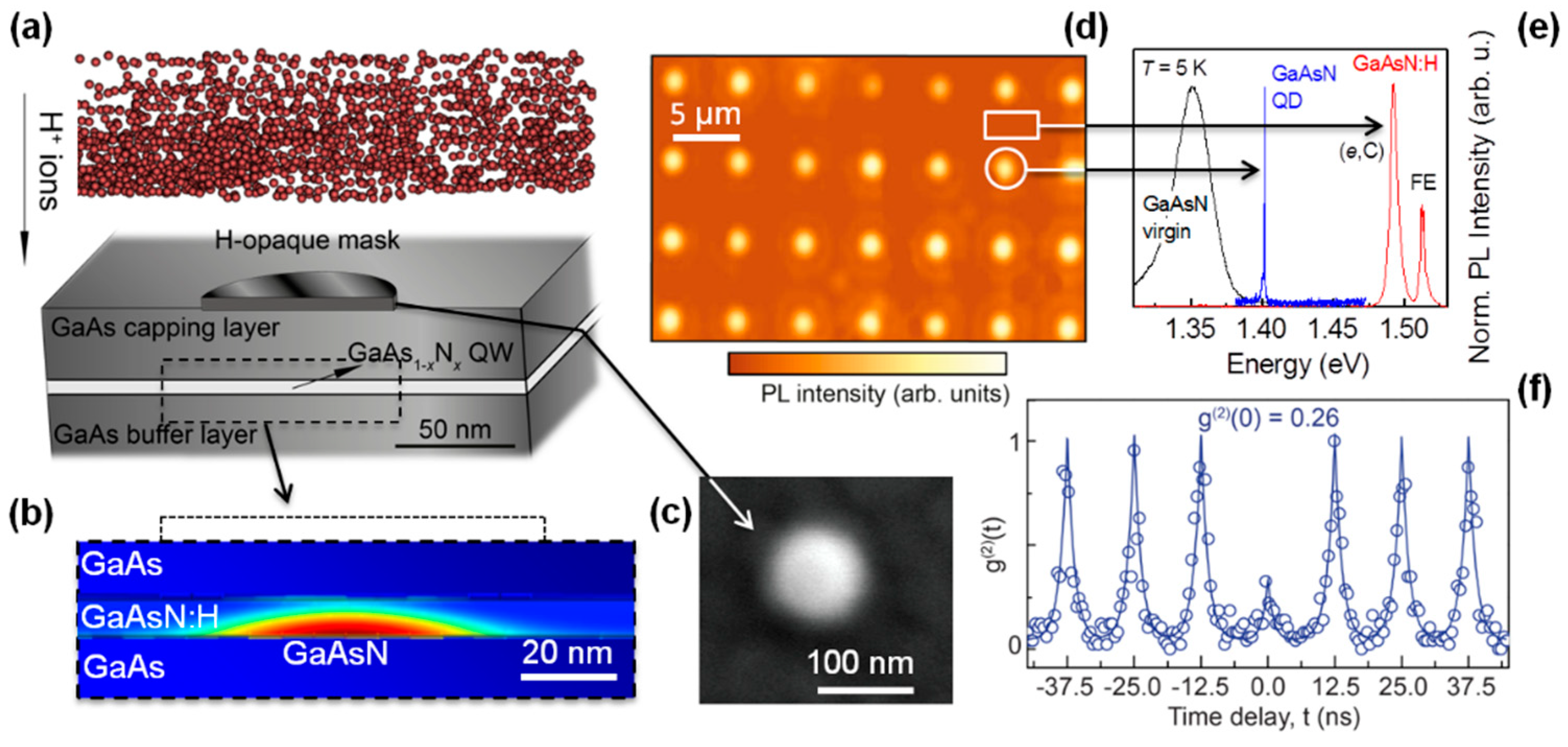
A schematic representation of the site-controlled dilute nitride QD fabrication process by spatially selective hydrogen incorporation is reported in Figure 4a–c. Such fabrication approach starts from a standard dilute nitride quantum well (e.g., GaAsN/GaAs) buried few tens of nanometers (typically 20–100 nm) below the sample surface. An isolated H-opaque circular mask is first patterned by electron-beam lithography (EBL) on the sample surface. The hydrogenation of such a patterned QW structure results in the spatially controlled diffusion of hydrogen inside the sample, and, eventually, in a well-defined spatial region of GaAsN material completely surrounded by a barrier of fully hydrogenated GaAsN (laterally) and GaAs (above and below). Due to a partial H diffusion beneath the mask, the actual size of the GaAsN region can be smaller than the physical size of the mask itself, as evident by finite-elements calculations of the post-hydrogenation distribution of electrically active N atoms (N atoms with no bound hydrogen); see Figure 4b [79]. Arrays of isolated circular masks of different diameter (ranging from 80 nm to 500 nm; see Figure 4c) were patterned by EBL with a negative-tone HSQ (hydrogen silsesquioxane) resist on top of a 6 nm-thick GaAsN/GaAs QW with a nitrogen concentration x = 1.1%, capped by a 30 nm-thick GaAs layer. The sample was then irradiated with hydrogen ions by means of a Kaufman source [81]. The ion-beam kinetic energy was set to a low value (100 eV) in order to minimize sample damage, whilst the sample was kept at a temperature of 190 °C for the entire duration of the irradiation process, to allow H diffusion inside the sample while maintaining an extremely sharp diffusion profile (hydrogen forefront ~5 nm/decade; see Figure 2 [69]). Different hydrogen doses were investigated in order to reach a full passivation of the open region and a well-defined GaAsN dot beneath the mask. At the end of the fabrication process, the H-opaque HSQ masks were removed by chemical etching in an aqueous solution of potassium borates (5–15%) and potassium hydroxide (2%), which dissolves HSQ but does not attack the sample, thus giving access to the optical characterization of the realized nanostructures.
Figure 4d shows a μPL image of an array of GaAsN dots obtained by employing mask dots of 80 nm. The μPL image demonstrates an excellent control over the dot position and exhibits a quite uniform emission efficiency. Furthermore, the entire process is highly scalable due to the use of electron-beam lithography. PL spectra were recorded on a single dot, showing one narrow line, and on the H-irradiated region in between GaAsN dots; see Figure 4e, in which the spectrum of the hydrogenated GaAsN barrier is indistinguishable from that of GaAs. Besides being site-controlled with a spatial accuracy equal to that of the EBL system (~20 nm—the EBL-defined HSQ pattern acts as a mask for H without the need for any further lithographic steps), the QDs obtained by the proposed techniques have also shown the ability to emit single photons on demand [80], see Figure 4f. They are, therefore, ideal candidates for a deterministic integration with nanophotonic devices.
3.2. QD Direct Writing by Near Field Illumination
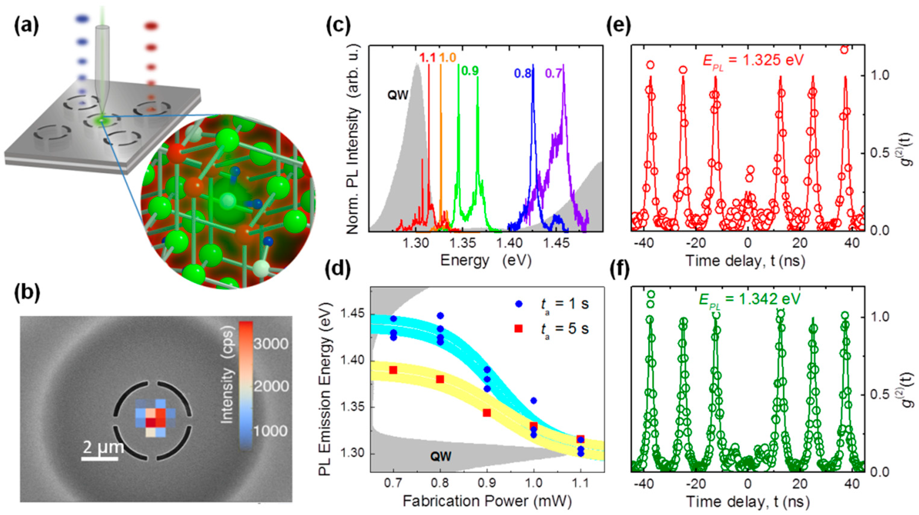
As shown in Section 2.3, in addition to the masked-hydrogenation procedure described above, another way to spatially control the hydrogen concentration in dilute nitrides can be obtained by local H removal via laser treatments. However, it is necessary to overcome the diffraction limit of objective lenses in order to employ such a strategy for QD fabrication [82]. Very recently, this goal was reached by shining a hydrogenated GaAsN sample through the tip of a scanning near-field optical microscope (SNOM), thus achieving spatial accuracy < 100 nm via a fully optical approach [30]. In order to test the QD fabrication process under conditions similar to those needed for the realization of an integrated QD-photonic crystal cavity system, the sample was processed with an array of well-separated circular areas in which the QW was suspended with respect to the substrate, as shown in Figure 5a,b. The fabrication of the suspended membrane follows the same steps required for the realization of a photonic crystal cavity and will be described in the next section. The QD fabrication was performed by exposing for a few seconds a nanometric region of the membrane surface, ideally the central region, with the 514.5 nm line of a continuous wave argon laser by means of the SNOM dielectric tip. Exploiting the optical near field of the tip, we aim to remove hydrogen from the GaAsN:H layer of the QW in an area (~100 nm) much smaller than the typical spot size (about 500 nm) obtained at this wavelength with a high NA objective lens (see, e.g., Figure 3). The fabrication power (Pa) and exposure time (ta) are varied to optimize the fabrication process; by doing this, it was possible to get fine control not only of the spatial position but also of the emission energy of the created QDs. In Figure 5c, we have reported the PL spectra of five representative GaAsN QDs fabricated at different powers, from 1.1 mW to 0.7 mW, with the same exposure time (1 s). The PL spectrum of the GaAsN/GaAs QW before hydrogenation is also reported for comparison reasons, as the QW emission energy (about 1.30 eV in the specific case) represents the lower limit for the QD emission. Indeed, when hydrogen is removed from an area large enough that the H-induced confinement effects are negligible, the fabricated dots approach the QW’s behavior. This situation can be attained for either high fabrication powers or long exposure times. By keeping the exposure time fixed while reducing the fabrication power, indeed, the QD diameter is expected to decrease. In turn, this should result in a larger confinement-induced blueshift, as rather clearly observed in the data reported in Figure 5c,d. The inhomogeneous broadening of the emission energy of the realized QDs (~20 meV) is the same as the linewidth of the pristine GaAsN/GaAs QW, suggesting that such a value could be improved by using a higher quality QW. Also, the QDs obtained by near-field optical illumination emit in the single-photon regime, independently of the QD emission energy [30]; see Figure 5e,f.
4. Quantum Emitter Integration in Photonic Crystal Cavities
Coupling QDs with photonic structures, in particular with photonic crystal (PhC) cavities [1,5], is a fundamental step towards the practical implementation of quantum devices. Indeed, such a coupling increases the radiative recombination rate of the QD and the speed and brightness of the device, while it reduces the negative effects of dephasing [83,84], thereby greatly improving the performance of QDs as sources of single and entangled photons [1,5]. It can also help to couple light into waveguides aiming at realizing all-integrated optical chips. The stochastic coupling of self-assembled QDs to photonic crystal cavities has been demonstrated both in the weak [85] and strong coupling regime [86,87]. On the other hand, the strategy to deterministically align a photonic crystal cavity to a single QD was for years simply based on the fabrication of the cavity after the QD was located by microscopy techniques [24,25]. The methods presented here for the realization of dilute nitride-based, site-controlled quantum emitters rely on top-down approaches that provide clear advantages over current state-of-the-art techniques in terms of flexibility and because they open the way to a unique possibility to fabricate QDs in specified points of an existing, optimized photonic structure. In particular, the spatially selective hydrogen incorporation described in Section 3.1 has already been applied successfully to the fabrication of a QD-PhC cavity system, in which the weak-coupling regime has been observed [28,29]. These recent results are reviewed in the following.
Lithographic Approach for QD-PhC Cavity Integration
Aiming at obtaining a deterministic integration of a quantum emitter with a photonic crystal cavity—with state-of-the-art spatial accuracy (see Table 1)—we developed a fully lithographic approach to fabricate QD-PhC cavity integrated systems, which relies on the realignment precision of the EBL system (~20 nm) on a series of alignment markers present on the sample surface.
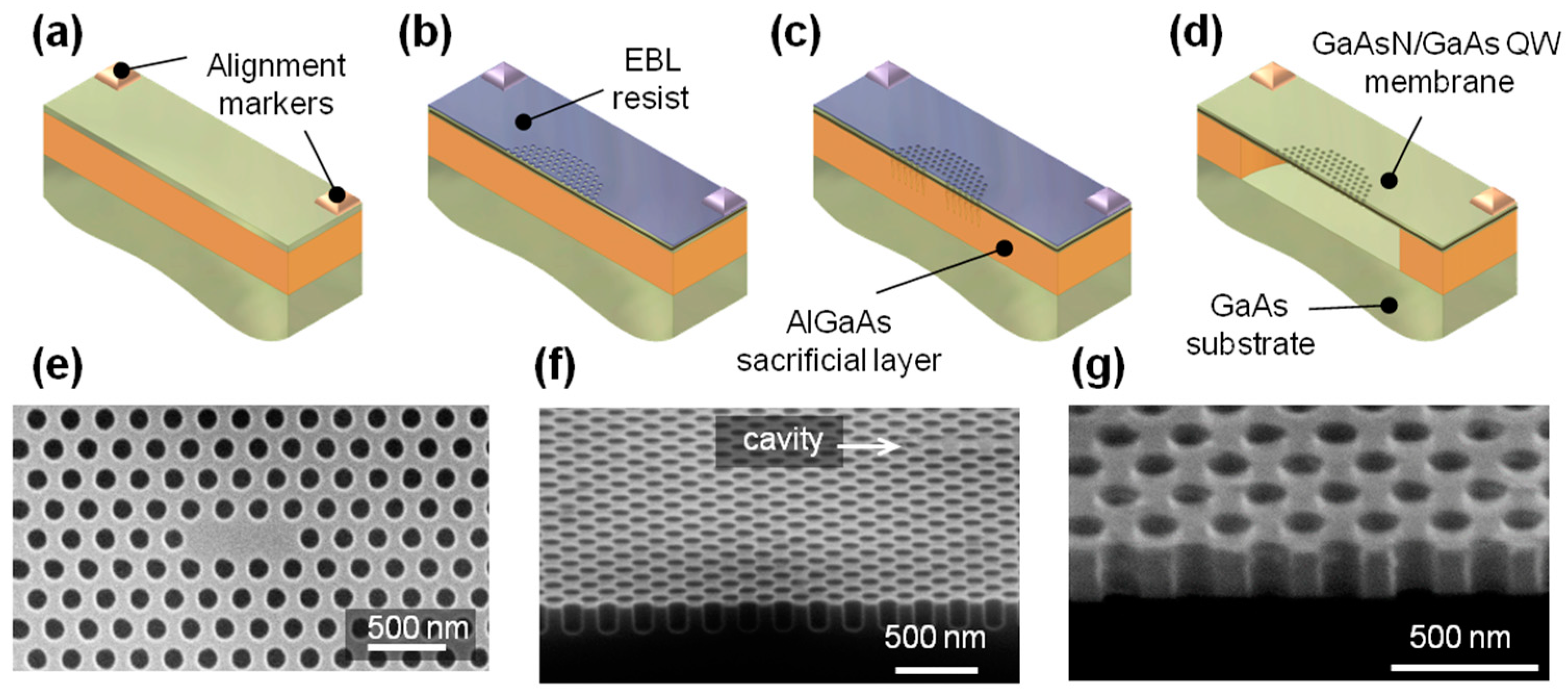
The fabrication process is sketched in Figure 6. The sample is first provided with a series of Cr/Au alignment markers by means of a standard lift-off process; see Figure 6a. Then, it is covered with a thin layer of positive-tone electron-beam resist (ZEP520A) on which the desired PhC cavity pattern is realized by electron-beam lithography; see Figure 6b. The resist acts as a mask during the transfer of the PhC design onto the sample via Cl-based dry etching of the GaAsN/GaAs layer; see Figure 6c. Finally, the mask resist is removed by a wet etching in hot anisole and the membrane containing the PhC structure is released by wet etching of the AlGaAs sacrificial layer with a 5% solution of hydrofluoric acid, in order to provide vertical optical isolation; see Figure 6d. A GaAsN QD can be realized either before the realization of the PhC cavity (i.e., soon after the deposition of the alignment markers) or after the complete realization of the PhC cavity, by making use of the spatially selective hydrogenation approach described in Section 3.1. In both cases, the presence of the alignment markers on the sample—together with the spatial accuracy in defining the QD and PhC cavity given by the EBL—guarantees a spatial coupling between the QD and the cavity of about 20 nm (limited only by the realignment precision of the EBL system). Further details on the fabrication process can be found in Ref. [28].
We want to stress here that a QD-PhC integrated system might also be realized by using the spatially selective hydrogen-removal approach presented in Section 3.2. In this case, indeed, the SNOM ability to “see” the electromagnetic field of a PhC cavity [88] can be used to map the field distribution of the fundamental cavity mode of a fully hydrogenated GaAsN/GaAs PhC cavity and, eventually, to fabricate by near field illumination a quantum emitter coupled with the cavity mode. Although within this further approach the spatial accuracy is worse than that achievable with the EBL-based method presented above (only a spatial precision of ~100 nm can be reached by conventional SNOM’s stages), the overall process flexibility is improved by the possibility to tailor the emission energy of the QD to that of the cavity mode simply by varying the QD fabrication parameters (see Figure 5).
As summarized in Figure 7, integrated QD-PhC cavity systems have already been successfully realized using a fully lithographic approach [28]. The energy of the fundamental cavity mode (CM) of a series of L3 photonic defects (wherein the microcavity is obtained by removing three holes from an otherwise perfectly periodic photonic lattice [89]; see Figure 6e,g) was lithographically tuned into resonance with the QD emission by adjusting the PhC lattice pitch (a); see Figure 7c. After achieving a coarse spectral matching between the CM and the QD exciton (X) for a = 255 nm, the system was progressively tuned into resonance by varying the sample temperature T, as displayed in Figure 7a. This was made possible by the much stronger T dependence of the energy of the X transition, which follows the band gap reduction of GaAsN with T [90], with respect to the CM, which linearly redshifts (at a rate of ~20 μeV/K, consistent with Refs. [91]) due to the variation of the refractive index of GaAs with T. An interesting outcome of the progressive reduction of the QD-CM energy detuning with T is reported in Figure 7b, which displays the temperature dependence of the micro-PL intensity of the QD and CM peaks. As T is increased from 10 K to 50 K, the PL signal shows the intensity drop-off usually expected in semiconducting samples, chiefly due to the thermal activation of non-radiative recombination channels [92]. For T > 50 K, however, a large increase in the PL intensity can be observed as the X line is moved into resonance with the CM. This is consistent with the ~10-fold enhancement of the radiative recombination rate (i.e., the Purcell effect [93]) measured for this system [29].
As regards the properties of the quantum emitter integrated in the cavity, it is important to stress that also in this condition the site-controlled QD is able to emit at the single photon regime, which is a crucial property for the successful employment of these systems in future applications. Evidence of such a non-classical behavior of light is given by the observation of a strong antibunching for near-zero time delay in the autocorrelation histogram of the QD exciton emission line reported in Figure 7d.
5. Conclusions and Perspectives
In summary, the possibility to finely control the spatial incorporation and/or removal of hydrogen in dilute nitride semiconductors has opened the way to a novel, versatile fabrication technique for site-controlled quantum emitters. The site-controlled QDs fabricated by tailoring the energy gap of dilute nitrides in their growth plane, have shown, indeed, the ability to emit single photons on demand. Those QDs have also evidenced the presence of both exciton and biexciton emissions in their PL spectra [30,80], a prerequisite for the possible generation of entangled photon pairs. In addition, the possibility to modulate the optoelectronic properties of dilute nitride semiconductors by spatially selective hydrogenation, and consequently to control the refractive index of the material with sub-wavelength resolution [63,94], might provide an ideal platform for the fabrication of integrated photonic circuits, providing an innovative way to define the optical elements—such as waveguides, beam splitters, and phase shifters—, which are required for the manipulation of photonic qubits.
The fabricated QDs have also been deterministically coupled with photonic crystal cavities, proving their inherent suitability to act as integrated light sources in complex nanophotonic devices. In particular, the presented lithographic approach exhibits an unparalleled spatial matching (~20 nm) between the emitter and the cavity, thanks to the high spatial resolution made available by electron-beam lithography, whilst a good spectral matching (~20–30 meV) is achieved via the fine lithographic tuning of the PhC lattice constant (i.e., cavity-mode energy), or, eventually, by controlling the emission energy of the QDs through their fabrication by near-field optical illumination (as presented in Section 3.2). While the ability to deterministically integrate dilute nitride-based QDs with photonic devices was demonstrated for photonic crystal cavities, of course the techniques described here may also be applied to other kinds of micro-cavities, like, for example, microdisk or micropillar ones, which have been reported to provide single photon devices with very high performances [26,95].
In this paper we reviewed mainly results obtained on GaAsN samples with [N] ~ 1%; nevertheless, it is worth mentioning that those results could be extended to obtain integrated systems working at wavelengths of interest for telecommunication applications simply by using samples with a larger nitrogen content ([N] ~ 4%) or, alternatively, by using an InGaAsN QW sample [96] instead of a GaAsN one.
Acknowledgments
We acknowledge colleagues who have contributed to different stages of the research presented here; in particular: F.I., A.V., and M.G. (LENS and University of Florence, Italy) for time-resolved and SNOM experiments; A.G. (CNR-IFN, Italy) for sample processing by electron-beam lithography; N.B. and A.P. (The University of Nottingham, UK) for laser annealing experiments; and D.G. (Fondazione Bruno Kessler, Italy) for SIMS measurements. Finally, we thank F.M. (CNR-IMM, Italy), S.R. (CNR-IOM, Italy), and M.H. (University of Sheffield, UK) for growing most of the samples. Part of this work was supported by Italian Ministry for Education, University and Research within the Futuro in Ricerca (FIRB) program (project DeLIGHTeD, Protocollo RBFR12RS1W).
Conflicts of Interest
The authors declare no conflict of interest. The funding sponsor had no role in the design of the study; in the collection, analyses, or interpretation of data; in the writing of the manuscript; or in the decision to publish the results.
References
- Lodahl, P.; Mahmoodian, S.; Stobbe, S. Interfacing single photons and single quantum dots with photonic nanostructures. Rev. Mod. Phys. 2015, 87, 347–400. [Google Scholar] [CrossRef]
- Somaschi, N.; Giesz, V.; De Santis, L.; Loredo, J.C.; Almeida, M.P.; Hornecker, G.; Portalupi, S.L.; Grange, T.; Antón, C.; Demory, J.; et al. Near-optimal single-photon sources in the solid state. Nat. Photonics 2016, 10, 340–345. [Google Scholar] [CrossRef]
- Klimov, V.I. Nanocrystal Quantum Dots; CRC Press: Boca Raton, FL, USA, 2010; ISBN 10 1420079263. [Google Scholar]
- Sattler, K.D. Handbook of Nanophysics: Nanoparticles and Quantum Dots; CRC Press: Boca Raton, FL, USA, 2010; ISBN 978142007544. [Google Scholar]
- Michler, P. Single Semiconductor Quantum Dots; Springer: Berlin/Heidelberg, Germany, 2009; ISBN 978-3-540-87445-4. [Google Scholar]
- Stangl, J.; Holy, V.; Bauer, G. Structural properties of self-organized semiconductor nanostructures. Rev. Mod. Phys. 2004, 76, 725–783. [Google Scholar] [CrossRef]
- Schmidt, O.G. Lateral Alignment of Epitaxial Quantum Dots; Springer: Berlin, Germany, 2007; ISBN 978-3-540-46936-0. [Google Scholar]
- Hartmann, A.; Loubies, L.; Reinhardt, F.; Kapon, E. Self-limiting growth of quantum dot heterostructures on nonplanar {111}B substrates. Appl. Phys. Lett. 1997, 71, 1314–1316. [Google Scholar] [CrossRef]
- Sugiyama, Y.; Sakuma, Y.; Muto, S.; Yokoyama, N. Novel InGaAs/GaAs quantum dot structures formed in tetrahedral-shaped recesses on (111)B GaAs substrate using metalorganic vapor phase epitaxy. Appl. Phys. Lett. 1995, 67, 256–258. [Google Scholar] [CrossRef]
- Surrente, A.; Felici, M.; Gallo, P.; Rudra, A.; Dwir, B.; Kapon, E. Dense arrays of site-controlled quantum dots with tailored emission wavelength: Growth mechanisms and optical properties. Appl. Phys. Lett. 2017, 111, 221102. [Google Scholar] [CrossRef]
- Gallo, P.; Felici, M.; Dwir, B.; Atlasov, K.A.; Karlsson, K.F.; Rudra, A.; Mohan, A.; Biasiol, G.; Sorba, L.; Kapon, E. Integration of site-controlled pyramidal quantum dots and photonic crystal membrane cavities. Appl. Phys. Lett. 2008, 92, 263101. [Google Scholar] [CrossRef]
- Poole, P.J.; Dalacu, D.; Lefebvre, J.; Williams, R.L. Selective epitaxy of semiconductor nanopyramids for Nanophotonics. Nanotechnology 2010, 21, 295302. [Google Scholar] [CrossRef] [PubMed]
- Chithrani, D.; Williams, R.L.; Lefebvre, J.; Poole, P.J.; Aers, G.C. Optical spectroscopy of single, site-selected, InAs/InP self-assembled quantum dots. Appl. Phys. Lett. 2004, 84, 978–980. [Google Scholar] [CrossRef]
- Dalacu, D.; Mnaymneh, K.; Sazonova, V.; Poole, P.J.; Aers, G.C.; Lapointe, J.; Cheriton, R.; SpringThorpe, A.J.; Williams, R. Deterministic emitter-cavity coupling using a single-site controlled quantum dot. Phys. Rev. B 2010, 82, 033301. [Google Scholar] [CrossRef]
- Jeppesen, S.; Miller, M.S.; Kowalski, B.; Maximov, I.; Samuelson, L. InAs quantum dots in GaAs holes: Island number dependence on hole diameter and conduction-band coupling estimates. Superlattices Microstruct. 1998, 23, 1347–1352. [Google Scholar] [CrossRef]
- Atkinson, P.; Ward, M.B.; Bremner, S.P.; Anderson, D.; Farrow, T.; Jones, G.A.C.; Shields, A.J.; Ritchie, D.A. Site-Control of InAs Quantum Dots using Ex-Situ Electron-Beam Lithographic Patterning of GaAs Substrates. Jpn. J. Appl. Phys. 2006, 45, 2519. [Google Scholar] [CrossRef]
- Jöns, K.D.; Atkinson, P.; Müller, M.; Heldmaier, M.; Ulrich, S.M.; Schmidt, O.G.; Michler, P. Triggered Indistinguishable Single Photons with Narrow Line Widths from Site-Controlled Quantum Dots. Nano Lett. 2013, 13, 126–130. [Google Scholar] [CrossRef] [PubMed]
- Jamil, A.; Skiba-Szymanska, J.; Kalliakos, S.; Schwagmann, A.; Ward, M.B.; Brody, Y.; Ellis, D.J.P.; Farrer, I.; Griffiths, J.P.; Jones, G.A.C.; et al. On-chip generation and guiding of quantum light from a site-controlled quantum dot. Appl. Phys. Lett. 2014, 104, 101108. [Google Scholar] [CrossRef]
- Braun, T.; Schneider, C.; Maier, S.; Igusa, R.; Iwamoto, S.; Forchel, A.; Höfling, S.; Arakawa, Y.; Kamp, M. Temperature dependency of the emission properties from positioned In(Ga)As/GaAs quantum dots. AIP Adv. 2014, 4, 097128. [Google Scholar] [CrossRef] [Green Version]
- Kohmoto, S.; Nakamura, H.; Ishikawa, T.; Asakawa, K. Site-controlled self-organization of individual InAs quantum dots by scanning tunneling probe-assisted nanolithography. Appl. Phys. Lett. 1999, 75, 3488–3490. [Google Scholar] [CrossRef]
- Kitamura, M.; Nishioka, M.; Oshinowo, J.; Arakawa, Y. In situ fabrication of self-aligned InGaAs quantum dots on GaAs multiatomic steps by metalorganic chemical vapor deposition. Appl. Phys. Lett. 1995, 66, 3663–3665. [Google Scholar] [CrossRef]
- Lee, H.; Johnson, J.A.; Speck, J.S.; Petroff, P.M. Controlled ordering and positioning of InAs self-assembled quantum dots. J. Vac. Sci. Technol. B 2000, 18, 2193–2196. [Google Scholar] [CrossRef]
- Kalliakos, S.; García, C.P.; Pellegrini, V.; Zamfirescu, M.; Cavigli, L.; Gurioli, M.; Vinattieri, A.; Pinczuk, A.; Dennis, B.S.; Pfeiffer, L.N.; West, K.W. Photoluminescence of individual doped GaAs/AlGaAs nanofabricated quantum dots. Appl. Phys. Lett. 2007, 90, 181902. [Google Scholar] [CrossRef]
- Hennessy, K.; Badolato, A.; Winger, M.; Gerace, D.; Atatüre, M.; Gulde, S.; Fält, S.; Hu, E.L.; Imamoğlu, A. Quantum nature of a strongly coupled single quantum dot–cavity system. Nature 2007, 445, 896–899. [Google Scholar] [CrossRef] [PubMed]
- Dousse, A.; Lanco, L.; Suffczyňski, J.; Semenova, E.; Miard, A.; Lemaître, A.; Sagnes, I.; Roblin, C.; Bloch, J.; Senellart, P. Controlled Light-Matter Coupling for a Single Quantum Dot Embedded in a Pillar Microcavity Using Far-Field Optical Lithography. Phys. Rev. Lett. 2008, 101, 267404. [Google Scholar] [CrossRef] [PubMed]
- Senellart, P.; Solomon, G.; White, A. High-performance semiconductor quantum-dot single-photon sources. Nat. Nanotechnol. 2017, 12, 1026–1039. [Google Scholar] [CrossRef] [PubMed]
- He, Y.-M.; Liu, J.; Maier, S.; Emmerling, M.; Gerhard, S.; Davanço, M.; Srinivasan, K.; Schneider, C.; Höfling, S. Deterministic implementation of a bright, on-demand single-photon source with near-unity indistinguishability via quantum dot imaging. Optica 2017, 4, 802–808. [Google Scholar] [CrossRef] [PubMed]
- Pettinari, G.; Gerardino, A.; Businaro, L.; Polimeni, A.; Capizzi, M.; Hopkinson, M.; Rubini, S.; Biccari, F.; Intonti, F.; Vinattieri, A.; et al. A lithographic approach for quantum dot-photonic crystal nanocavity coupling in dilute nitrides. Microelectron. Eng. 2017, 174, 16–19. [Google Scholar] [CrossRef]
- Felici, M.; Pettinari, G.; Biccari, F.; Boschetti, A.; Birindelli, S.; Younis, S.; Gurioli, M.; Vinattieri, A.; Gerardino, A.; Businaro, L.; et al. Broadband enhancement of light-matter interaction in photonic crystal cavities integrating site-controlled Ga(AsN)/Ga(AsN):H quantum dots. Phys. Rev. X 2018. under review. [Google Scholar]
- Biccari, F.; Boschetti, A.; Pettinari, G.; La China, F.; Gurioli, M.; Intonti, F.; Vinattieri, A.; Sharma, M.S.; Capizzi, M.; Gerardino, A.; et al. Site-controlled single photon emitters fabricated by near field illumination. Adv. Mater 2018, in press. [Google Scholar] [CrossRef] [PubMed]
- Ciatto, G. Hydrogenated Dilute Nitride Semiconductors; Pan Stanford Publishing: Singapore, 2015; ISBN 978-981-4463-45-4. [Google Scholar]
- Buyanova, I.A.; Chen, W.M. Physics and Applications of Dilute Nitrides; Taylor & Francis: New York, NY, USA, 2004; ISBN 1591690196. [Google Scholar]
- Henini, M. Dilute Nitride Semiconductors: Physics and Technology; Elsevier: New York, NY, USA, 2005; ISBN 9780080445021. [Google Scholar]
- Ayse, E. Dilute III-V Nitride Semiconductors and Material Systems; Springer: Berlin, Germany, 2008; ISBN 978-3-540-74529-7. [Google Scholar]
- O’Reilly, E.P.; Lindsay, A.; Klar, P.J.; Polimeni, A.; Capizzi, M. Trends in the electronic structure of dilute nitride alloys. Semicond. Sci. Technol. 2009, 24, 033001. [Google Scholar] [CrossRef]
- Kent, P.R.C.; Zunger, A. Evolution of III-V nitride alloy electronic structure: The localized to delocalized transition. Phys. Rev. Lett. 2001, 86, 2613–2616. [Google Scholar] [CrossRef] [PubMed]
- Kent, P.R.C.; Zunger, A. Theory of electronic structure evolution in GaAsN and GaPN alloys. Phys. Rev. B 2001, 64, 115208. [Google Scholar] [CrossRef]
- Tisch, U.; Finkman, E.; Salzman, J. The anomalous bandgap bowing in GaAsN. Appl. Phys. Lett. 2002, 81, 463–465. [Google Scholar] [CrossRef]
- Masia, F.; Pettinari, G.; Polimeni, A.; Felici, M.; Miriametro, A.; Capizzi, M.; Lindsay, A.; Healy, S.B.; O’Reilly, E.P.; Cristofoli, A.; et al. Interaction between conduction band edge and nitrogen states probed by carrier effective-mass measurements in GaAs1−xNx. Phys. Rev. B 2006, 73, 073201. [Google Scholar] [CrossRef]
- Allison, G.; Spasov, S.; Patanè, A.; Eaves, L.; Kozlova, N.V.; Freudenberger, J.; Hopkinson, M.; Hill, G. Electron effective mass and Si-donor binding energy in GaAs1−xNx probed by a high magnetic field. Phys. Rev. B 2008, 77, 125210. [Google Scholar] [CrossRef]
- Dannecker, T.; Jin, Y.; Cheng, H.; Gorman, C.F.; Buckeridge, J.; Uher, C.; Fahy, S.; Kurdak, C.; Goldman, R.S. Nitrogen composition dependence of electron effective mass in GaAs1−xNx. Phys. Rev. B 2010, 82, 125203. [Google Scholar] [CrossRef]
- Pettinari, G.; Masia, F.; Polimeni, A.; Felici, M.; Frova, A.; Capizzi, M.; Lindsay, A.; O’Reilly, E.P.; Klar, P.J.; Stolz, W.; et al. Influence of nitrogen-cluster states on the gyromagnetic factor of electrons in GaAs1−xNx. Phys. Rev. B 2006, 74, 245202. [Google Scholar] [CrossRef]
- Ivchenko, E.L.; Kalevich, V.K.; Shiryaev, A.Y.; Afanasiev, M.M.; Masumoto, Y. Optical orientation and spin-dependent recombination in GaAsN alloys under continuous-wave pumping. J. Phys. Cond. Matter 2010, 22, 465804. [Google Scholar] [CrossRef] [PubMed]
- Kunold, A.; Balocchi, A.; Zhao, F.; Amand, T.; Ben Abdallah, N.; Harmand, J.C.; Marie, X. Giant spin-dependent photo-conductivity in GaAsN dilute nitride semiconductor. Phys. Rev. B 2011, 83, 165202. [Google Scholar] [CrossRef]
- Klar, P.J.; Grüning, H.; Heimbrodt, W.; Koch, J.; Höhnsdorf, F.; Stolz, W.; Vicente, P.M.A.; Camassel, J. From N isoelectronic impurities to N-induced bands in the GaNxAs1−x alloy. Appl. Phys. Lett. 2000, 76, 3439–3441. [Google Scholar] [CrossRef]
- Weinstein, B.A.; Stambach, S.R.; Ritter, T.M.; Maclean, J.O.; Wallis, D.J. Evidence for selective delocalization of N-pair states in dilute GaAs1−xNx. Phys. Rev. B 2003, 68, 035336. [Google Scholar] [CrossRef]
- Pettinari, G.; Polimeni, A.; Masia, F.; Trotta, R.; Felici, M.; Capizzi, M.; Niebling, T.; Stolz, W.; Klar, P.J. Electron mass in dilute nitrides and its anomalous dependence on hydrostatic pressure. Phys. Rev. Lett. 2007, 98, 146402. [Google Scholar] [CrossRef] [PubMed]
- Polimeni, A.; Capizzi, M.; Geddo, M.; Fischer, M.; Reinhardt, M.; Forchel, A. Effect of nitrogen on the temperature dependence of the energy gap in InxGa1−xAs1−yNy/GaAs single quantum wells. Phys. Rev. B 2001, 63, 195320. [Google Scholar] [CrossRef]
- Luo, X.D.; Xu, Z.Y.; Ge, W.K.; Pan, Z.; Li, L.H.; Lin, Y.W. Photoluminescence properties of a GaN0.015As0.985/GaAs single quantum well under short pulse excitation. Appl. Phys. Lett. 2001, 79, 958–960. [Google Scholar] [CrossRef]
- Pettinari, G.; Felici, M.; Trotta, R.; Capizzi, M.; Polimeni, A. Hydrogen effects in dilute III-N-V alloys: From defect engineering to nanostructuring. J. Appl. Phys. 2014, 115, 012011. [Google Scholar] [CrossRef]
- Pearton, S.J.; Corbett, J.W.; Stavola, M. Hydrogen in Crystalline Semiconductors; Springer Series in Materials Science; Springer: Berlin, Germany, 1992; Volume 16. [Google Scholar]
- Pankove, J.I.; Johnson, N.M. Hydrogen in Semiconductors. In Semiconductors and Semimetals; Academic: New York, NY, USA, 1991; Volume 34. [Google Scholar]
- Pettinari, G.; Patanè, A.; Polimeni, A.; Capizzi, M.; Lu, X.; Tiedje, T. Effects of hydrogen on the electronic properties of Ga(AsBi) alloys. Appl. Phys. Lett. 2012, 101, 222103. [Google Scholar] [CrossRef]
- Pettinari, G.; Filippone, F.; Polimeni, A.; Mattioli, G.; Patanè, A.; Lebedev, V.; Capizzi, M.; Amore Bonapasta, A. Genesis of “Solitary Cations” Induced by Atomic Hydrogen. Adv. Funct. Mater. 2015, 25, 353–5359. [Google Scholar] [CrossRef]
- Kozlova, N.V.; Pettinari, G.; Makarovsky, O.; Mori, N.; Polimeni, A.; Capizzi, M.; Zhuang, Q.D.; Krier, A.; Patanè, A. Nonresonant hydrogen dopants in In(AsN): A route to high electron concentrations and mobilities. Phys. Rev. B 2013, 87, 165207. [Google Scholar] [CrossRef]
- Bissiri, M.; Baldassarri Höger von Högersthal, G.; Polimeni, A.; Gaspari, V.; Ranalli, F.; Capizzi, M.; Amore Bonapasta, A.; Jiang, F.; Stavola, M.; Gollub, D.; et al. Hydrogen induced passivation of nitrogen in GaAs1−yNy. Phys. Rev. B 2002, 65, 235210. [Google Scholar] [CrossRef]
- Polimeni, A.; Baldassarri Höger von Högersthal, G.; Bissiri, M.; Capizzi, M.; Frova, A.; Fischer, M.; Reinhardt, M.; Forchel, A. Role of hydrogen in III-N-V compound semiconductors. Semicond. Sci. Technol. 2002, 17, 797. [Google Scholar] [CrossRef]
- Klar, P.J.; Grüning, H.; Güngerich, M.; Heimbrodt, W.; Koch, J.; Torunski, T.; Stolz, W.; Polimeni, A.; Capizzi, M. Global changes of the band structure and the crystal lattice of Ga(N,As) due to hydrogenation. Phys. Rev. B 2003, 67, 121206. [Google Scholar] [CrossRef]
- Polimeni, A.; Baldassarri, H.V.H.G.; Bissiri, H.M.; Capizzi, M.; Fischer, M.; Reinhardt, M.; Forchel, A. Effect of hydrogen on the electronic properties of InxGa1−xAs1−yNy/GaAs quantum wells. Phys. Rev. B 2001, 63, 201304. [Google Scholar] [CrossRef]
- Baldassarri, H.V.H.G.; Bissiri, M.; Polimeni, A.; Capizzi, M.; Fischer, M.; Reinhardt, M.; Forchel, A. Hydrogen-induced band gap tuning of (InGa)(AsN)/GaAs single quantum wells. Appl. Phys. Lett. 2001, 78, 3472–3474. [Google Scholar] [CrossRef]
- Polimeni, A.; Bissiri, M.; Felici, M.; Capizzi, M.; Buyanova, I.A.; Chen, W.M.; Xin, H.P.; Tu, C.W. Nitrogen passivation induced by atomic hydrogen: The GaP1−yNy case. Phys. Rev. B 2003, 67, 201303. [Google Scholar] [CrossRef]
- Polimeni, A.; Masia, F.; Pettinari, G.; Trotta, R.; Felici, M.; Capizzi, M.; Lindsay, A.; O’Reilly, E.P.; Niebling, T.; Stolz, W.; et al. Role of strain and properties of N clusters at the onset of the alloy limit in GaAs1−xNx. Phys. Rev. B 2008, 77, 155213. [Google Scholar] [CrossRef]
- Trotta, R.; Polimeni, A.; Capizzi, M. Hydrogen Incorporation in III-N-V Semiconductors: From Macroscopic to Nanometer Control of the Materials’ Physical Properties. Adv. Funct. Mater. 2012, 22, 1782–1801. [Google Scholar] [CrossRef]
- Wen, L.; Bekisli, F.; Stavola, M.; Fowler, W.B.; Trotta, R.; Polimeni, A.; Capizzi, M.; Rubini, S.; Martelli, F. Detailed structure of the H-N-H center in GaAs1-yNy revealed by vibrational spectroscopy under uniaxial stress. Phys. Rev. B 2010, 81, 233201. [Google Scholar] [CrossRef]
- Ciatto, G.; Boscherini, F.; Amore Bonapasta, A.; Filippone, F.; Polimeni, A.; Capizzi, M. Nitrogen-hydrogen complex in GaAsxN1−x revealed by x-ray absorption spectroscopy. Phys. Rev. B 2005, 71, 201301. [Google Scholar] [CrossRef]
- Fowler, W.B.; Martin, K.R.; Washer, K.; Stavola, M. Structure and vibrational properties of N-H2 complexes in GaAs:N. Phys. Rev. B 2005, 72, 035208. [Google Scholar] [CrossRef]
- Du, M.-H.; Limpijumnong, S.; Zhang, S.B. Hydrogen pairs and local vibrational frequencies in H-irradiated GaAs1−yNy. Phys. Rev. B 2005, 72, 073202. [Google Scholar] [CrossRef]
- Amore Bonapasta, A.; Filippone, F.; Mattioli, G. H-Induced dangling bonds in H–isoelectronic-impurity complexes formed in GaAs1−yNy alloys. Phys. Rev. Lett. 2007, 98, 206403. [Google Scholar] [CrossRef] [PubMed]
- Trotta, R.; Giubertoni, D.; Polimeni, A.; Bersani, M.; Capizzi, M.; Martelli, F.; Rubini, S.; Bisognin, G.; Berti, M. Hydrogen diffusion in GaAs1−xNx. Phys. Rev. B 2009, 80, 195206. [Google Scholar] [CrossRef]
- Bissiri, M.; Baldassarri Höger von Högersthal, G.; Polimeni, A.; Capizzi, M.; Gollub, D.; Fischer, M.; Reinhardt, M.; Forchel, A. Role of N clusters in InxGa1−xAs1−yNy band-gap reduction. Phys. Rev. B 2002, 66, 033311. [Google Scholar] [CrossRef]
- Felici, M.; Polimeni, A.; Salviati, G.; Lazzarini, L.; Armani, N.; Masia, F.; Capizzi, M.; Martelli, F.; Lazzarino, M.; Bais, G.; et al. In-Plane Bandgap Engineering by Modulated Hydrogenation of Dilute Nitride Semiconductors. Adv. Mater. 2006, 18, 1993–1997. [Google Scholar] [CrossRef]
- Balakrishnan, N.; Pettinari, G.; Makarovsky, O.; Turyanska, L.; Fay, M.W.; De Luca, M.; Polimeni, A.; Capizzi, M.; Martelli, F.; Rubini, S.; et al. Band-gap profiling by laser writing of hydrogen-containing III-N-Vs. Phys. Rev. B 2012, 86, 155307. [Google Scholar] [CrossRef]
- Ciatto, G.; Pettinari, G.; Balakrishnan, N.; Berenguer, F.; Patanè, A.; Birindelli, S.; Felici, M.; Polimeni, A. Synchrotron x-ray diffraction study of micro-patterns obtained by spatially selective hydrogenation of GaAsN. Appl. Phys. Lett. 2015, 106, 051905. [Google Scholar] [CrossRef]
- Lax, M. Temperature rise induced by a laser beam. J.Appl. Phys. 1997, 48, 3919–3924. [Google Scholar] [CrossRef]
- Bisognin, G.; De Salvador, D.; Drigo, A.V.; Napolitani, E.; Sambo, A.; Berti, M.; Polimeni, A.; Felici, M.; Capizzi, M. Hydrogen-nitrogen complexes in dilute nitride alloys: Origin of the compressive lattice strain. Appl. Phys. Lett. 2006, 89, 061904. [Google Scholar] [CrossRef]
- Bisognin, G.; De Salvador, D.; Napolitani, E.; Berti, M.; Polimeni, A.; Capizzi, M.; Rubini, S.; Martelli, F.; Franciosi, A. High resolution X-ray diffraction in situ study of very small complexes: The case of hydrogenated dilute nitrides. J. Appl. Cryst. 2008, 41, 366–372. [Google Scholar] [CrossRef]
- Santos, P.V.; Johnson, N.M.; Street, R.A. Light-enhanced hydrogen motion in a-Si:H. Phys. Rev. Lett. 1991, 67, 2686–2689. [Google Scholar] [CrossRef] [PubMed]
- Loridant-Bernard, D.; Meziere, S.; Constant, M.; Dupuy, N.; Sombret, S.; Chevalier, J. Infrared study of light-induced reactivation of neutralized dopants in hydrogenated n-type GaAs doped with silicon. Appl. Phys. Lett. 1998, 73, 644–646. [Google Scholar] [CrossRef]
- Trotta, R.; Polimeni, A.; Martelli, F.; Pettinari, G.; Capizzi, M.; Felisari, L.; Rubini, S.; Francardi, M.; Gerardino, A.; Christianen, P.C.M.; et al. Fabrication of Site-Controlled Quantum Dots by Spatially Selective Incorporation of Hydrogen in Ga(AsN)/GaAs Heterostructures. Adv. Matter 2011, 23, 2706–2710. [Google Scholar] [CrossRef] [PubMed]
- Birindelli, S.; Felici, M.; Wildmann, J.S.; Polimeni, A.; Capizzi, M.; Gerardino, A.; Rubini, S.; Martelli, F.; Rastelli, A.; Trotta, R. Single Photons on Demand from Novel Site-Controlled GaAsN/GaAsN:H Quantum Dots. Nano Lett. 2014, 14, 1275–1280. [Google Scholar] [CrossRef] [PubMed]
- Kaufman, A. Broad-beam ion sources. Rev. Sci. Instrum. 1990, 61, 230–235. [Google Scholar] [CrossRef]
- Zayats, A.; Richards, D. Nano-Optics and Near-Field Optical Microscopy; Artech House: Norwood, MA, USA, 2009; ISBN 10 159693283X. [Google Scholar]
- Iles-Smith, J.; McCutcheon, D.P.S.; Nazir, A.; Mørk, J. Phonon scattering inhibits simultaneous near-unity efficiency and indistinguishability in semiconductor single-photon sources. Nat. Photonics 2017, 11, 521–526. [Google Scholar] [CrossRef]
- Grange, T.; Somaschi, N.; Antón, C.; De Santis, L.; Coppola, G.; Giesz, V.; Lemaître, A.; Sagnes, I.; Auffèves, A.; Senellart, P. Reducing Phonon-Induced Decoherence in Solid-State Single-Photon Sources with Cavity Quantum Electrodynamics. Phys. Rev. Lett. 2017, 118, 253602. [Google Scholar] [CrossRef] [PubMed]
- Englund, D.; Fattal, D.; Waks, E.; Solomon, G.; Zhang, B.; Nakaoka, T.; Arakawa, Y.; Yamamoto, Y.; Vučković, J. Controlling the Spontaneous Emission Rate of Single Quantum Dots in a Two-Dimensional Photonic Crystal. Phys. Rev. Lett. 2005, 95, 013904. [Google Scholar] [CrossRef] [PubMed]
- Yoshie, T.; Scherer, A.; Hendrickson, J.; Khitrova, G.; Gibbs, H.M.; Rupper, G.; Ell, C.; Shchekin, O.B.; Deppe, D.G. Vacuum Rabi splitting with a single quantum dot in a photonic crystal nanocavity. Nature 2004, 432, 200–203. [Google Scholar] [CrossRef] [PubMed]
- Englund, D.; Faraon, A.; Fushman, I.; Stoltz, N.; Petroff, P.; Vučković, J. Controlling cavity reflectivity with a single quantum dot. Nature 2007, 450, 857–861. [Google Scholar] [CrossRef] [PubMed]
- Caselli, N.; Intonti, F.; La China, F.; Riboli, F.; Gerardino, A.; Bao, W.; Bargioni, A.W.; Li, L.; Linfield, E.H.; Pagliano, F.; et al. Ultra-subwavelength phase-sensitive Fano-imaging of localized photonic modes. Light Sci. Appl. 2015, 4, e326. [Google Scholar] [CrossRef]
- Akahane, Y.; Mochizuki, M.; Asano, T.; Tanaka, Y.; Noda, S. Design of a channel drop filter by using a donor-type cavity with high-quality factor in a two-dimensional photonic crystal slab. Appl. Phys. Lett. 2003, 82, 1341–1343. [Google Scholar] [CrossRef] [Green Version]
- Polimeni, A.; Bissiri, M.; Augieri, A.; Baldassarri Hoger von Högersthal, G.; Capizzi, M.; Gollub, D.; Fischer, M.; Reinhardt, M.; Forchel, A. Reduced temperature dependence of the band gap in GaAs1−yNy investigated with photoluminescence. Phys. Rev. B 2002, 65, 235325. [Google Scholar] [CrossRef]
- Gevaux, D.G.; Bennett, A.J.; Stevenson, R.M.; Shields, A.J.; Atkinson, P.; Griffiths, J.; Anderson, D.; Jones, G.A.C.; Ritchie, D.A. Enhancement and suppression of spontaneous emission by temperature tuning InAs quantum dots to photonic crystal cavities. Appl. Phys. Lett. 2006, 88, 131101. [Google Scholar] [CrossRef]
- Pankove, J. Optical Processes in Semiconductors; Dover: New York, NY, USA, 1975; ISBN 10 0486602753. [Google Scholar]
- Purcell, E.M. Spontaneous Emission Probabilities at Radio Frequencies. Phys. Rev. 1946, 69, 681. [Google Scholar]
- Felici, M.; Pettinari, G.; Biccari, F.; Capizzi, M.; Polimeni, A. Spatially selective hydrogen irradiation of dilute nitride semiconductors: A brief review. Semicond. Sci. Technol. 2018, 33, 053001. [Google Scholar] [CrossRef]
- Portalupi, S.L.; Hornecker, G.; Giesz, V.; Grange, T.; Lemaître, A.; Demory, J.; Sagnes, I.; Lanzillotti-Kimura, N.D.; Lanco, L.; Auffèves, A.; et al. Bright Phonon-Tuned Single-Photon Source. Nano Lett. 2015, 15, 6290–6294. [Google Scholar] [CrossRef] [PubMed]
- Liu, H.Y.; Hopkinson, M.; Navaretti, P.; Gutierrez, M.; Ng, J.S.; David, J.P.R. Improving optical properties of 1.55 μm GaInNAs/GaAs multiple quantum wells with Ga(In)NAs barrier and space layer. Appl. Phys. Lett. 2003, 83, 4951–4953. [Google Scholar] [CrossRef]
Figure 1.
H-induced band-gap tuning in dilute nitrides. (a) Photoluminescence spectra at T = 10 K of a GaAsN/GaAs quantum well (width L = 6 nm) treated with increasing hydrogen doses dH; (b) same as in panel (a) for a GaAsN epilayer (thickness t = 110 nm) in the very dilute N concentration limit; (c) real colour photographic image of two GaPN epilayers (thickness t = 250 nm, [N] = 0.81%). The epilayer in the upper part of the picture was treated with two different hydrogen doses along its length, while the epilayer in the lower part of the picture was left untreated. The picture was acquired at T = 10 K, exciting the samples with the 458 nm line of an Ar+ laser. The change in colour clearly indicates a variation of the band gap energy upon hydrogenation. Panel (b) was reproduced with permission from [56]. Copyright 2002 The American Physical Society.

Figure 2.
N-H complex formation and spatial distribution. (a) Secondary-ion-mass spectrometry depth-profile of the deuterium concentration (the origin is set at the sample surface) for GaAsN samples with different N concentrations (x). Symbols and lines are experimental data and theoretical simulations, respectively. The sample irradiation temperature was TD = 300 °C; (b) same as in panel (a) for a x = 0.7% sample irradiated at different temperatures; (c) sketch of the nitrogen-hydrogen complex responsible for the electronic passivation of nitrogen in GaAsN. Panels (a,b) were adapted with permission from [69]. Copyright 2009 The American Physical Society. Panel (c) was reproduced with permission from [64]. Copyright 2010 The American Physical Society.

Figure 3.
Band-gap direct writing. (a) μPL maps at T = 300 K of a hydrogenated GaAsN/GaAs QW sample (dH = 6×1016 cm−2, [N] = 0.9%) following exposure for a time ta = 15 s to a focused laser beam with λa = 515 nm and Pa = 30 mW; The μPL spectra at positions A, B, C, and D are shown in panel (b). The μPL map is obtained by plotting the μPL intensity around E = 1.30 eV, corresponding to the peak energy of the QW emission in the virgin sample (see gray area in the μPL spectra), and was acquired with p = 1.2 mW and λ = 633 nm; (c) Examples of the capability to direct-write the band-gap energy of dilute nitrides at the micrometer scale, as given by H-shape and triangular-shape laser-written (Pa = 20 mW, ta = 20 s, λa= 532 nm) emitting areas mapped at 300 K with laser power of 0.5 mW; (d) Light-emitting spot created by laser writing (Pa = 20 mW, λa = 515 nm, and ta = 15 s) and mapped after a 1-hr thermal annealing in a high-temperature furnace at different temperatures. All μPL maps were obtained by integrating the PL intensity around the peak energy of the QW emission in the virgin sample (E = 1.30 eV); (e) N-H dissociation efficiency at the centre of the laser spot [i.e., position A in panel (a)] as a function of the annealing photon energy (lower scale) and wavelength (upper scale) at various power densities for ta = 20 s. Panel (c) was adapted with permission from [73]. Copyright 2015 AIP Publishing LLC. Panels (d,e) were adapted with permission from [72]. Copyright 2012 The American Physical Society.

Figure 4.
Site-controlled quantum emitters by spatially selective hydrogenation. (a) Hydrogen irradiation of a GaAsN/GaAs QW patterned with a nanometer-size H-opaque circular mask; (b) nanometer region of GaAsN surrounded by a barrier of GaAsN:H (laterally) and GaAs (above and below) resulting from the hydrogenation process; (c) SEM image of a single HSQ mask opaque to H (80 nm in diameter); (d) μPL image of an array or ordered GaAsN quantum emitters obtained by the technique depicted in panels (a–c). The image was recorded using an 850 nm low-energy pass filter to reject the emission from GaAs and hydrogenated GaAsN barriers. The single-dot image size is determined by the diffraction limit of the objective lens and by the carrier diffusion length. The μPL image demonstrates an excellent control over the dot position and a very uniform emission efficiency from the array; (e) μPL spectrum recorded on a single dot and on the barrier region that has been exposed to H irradiation; (f) normalized second-order correlation function for the excitonic emission of a single GaAsN dot. The amplitude of the zero-delay peak is well below the threshold value of 0.5, which points to the emission of single photons by the GaAsN QD. Panels (a–c) were adapted with permission from [28]. Copyright 2017 Elsevier. Panels (d,e) were adapted with permission from [79]. Copyright 2011 WILEY-VCH Verlag GmbH & Co. Panel (f) was adapted with permission from [80]. Copyright 2014 American Chemical Society.

Figure 5.
Site-controlled quantum emitters by near-field illumination. (a) Near-field optical illumination through the tip of a SNOM of the surface of a fully hydrogenated GaAsN/GaAs QW sample generates a hot spot within which the N-H bonds of the GaAsN:H layer are broken. This leaves a nanometer-sized region of GaAsN surrounded by a barrier of GaAsN:H (laterally) and GaAs (above and below); (b) top-view SEM image of a suspended GaAsN/GaAs QW structure (membrane), within which a QD has been fabricated as described in panel (a) (fabrication power of 1.1 mW for 1 s). The black areas are apertures opened in the membrane layer by dry etching, to allow a wet etching of the AlGaAs sacrificial layer and, consequently, the release of the suspended membrane containing the dilute nitride QW (see also Figure 6). In the SEM image, the circular region from which the sacrificial layer has been removed is visible as a dark-gray area underneath the released membrane. Superimposed to the SEM image is reported the PL intensity map at 10 K of the emission peak associated with the fabricated GaAsN QD (centered at 1.315 eV for this particular dot). The emission has a round shape and a spatial FWHM of 1 μm, equal to the setup resolution; (c) PL spectra at 10 K of different GaAsN QDs fabricated with different powers, distinguished by color (exposure time of 1 s). The PL spectrum of the GaAsN/GaAs QW before hydrogenation is also reported (gray areas). The fabrication powers, in units of mW, are provided as labels; (d) PL emission energy at 10 K of several GaAsN QDs as a function of the fabrication power. Blue dots and red squares represent 1 s and 5 s exposure time, respectively. The colored bands are a guide for the eye; (e,f) normalized second order autocorrelation function for two different QDs fabricated with the presented technique and having different emission energy (i.e., 1.325 eV and 1.342 eV). The value of g(2)(0) < 0.5 is a proof of the single photon emitter nature of the fabricated GaAsN QDs. Panels (b–f) were adapted with permission from [30]. Copyright 2018 WILEY-VCH Verlag GmbH & Co.

Figure 6.
Deterministic integration of a quantum emitter in a photonic crystal cavity. Sketch of the processing steps leading to the fabrication of an integrated QD-PhC cavity system: A series of alignment markers (Cr/Au) are first realized on the surface of a GaAsN/GaAs heterostructure by lift-off process (a); The sample is then covered with an EBL positive-tone resist (ZEP520A) and patterned by EBL with the required PhC design (b); The design is then transferred into the GaAsN/GaAs membrane layer by means of a Cl-based dry etching (c); Finally, the GaAs membrane is released by a HF wet etching of the AlGaAs sacrificial layer (d). SEM images of the sample at the end of the dry etching process [(e): tilted at 0° and (f): tilted at 75°] and after the release of the membrane [(g): tilted at 60°] are shown. A GaAsN QD can be realized either between steps (a,b) by making use of the spatially selective hydrogenation approach described in Figure 4, or after step (d) by a spatially selective hydrogenation approach (see Figure 4), as well as by a near-field illumination approach (see Figure 5). In the case of the spatially selective hydrogenation approach, it is possible to achieve a spatial coupling accuracy between the quantum emitter and the PhC cavity of about 20 nm, which is limited only by the realignment precision of the EBL system used. Adapted with permission from [28]. Copyright 2017 Elsevier.

Figure 7.
Characterization of the realized integrated QD-PhC cavity system. (a) Peak-normalized µPL spectra of an integrated QD-PhC cavity device, showing the temperature dependence of the cavity mode–quantum dot detuning. The exciton transition of the QD is labeled as X; (b) temperature dependence of the integrated PL intensity of the cavity mode (CM, black dots) and of the X peak (blue dots). The intensity increase observed for temperatures above ~ 50 K is a result of an increased QD-PhC cavity coupling (i.e., of the Purcell effect) due to the QD coming into resonance with the CM; (c) lithographic tuning of the CM energy of a PhC L3 defect cavity (r/a = 0.29) by varying the PhC lattice pitch value (a). Note the pretty good linear dependence (dECM/da ~ 3.5 meV/nm) of the CM energy with a; (d) second-order autocorrelation of the exciton ground-state transition for a site-controlled QD (mask diameter 160 nm) embedded in a PhC cavity. Note the g(2)(0) < 0.5, providing evidence of the single-photon emission regime for QDs integrated in PhC cavities. Adapted with permission from [28]. Copyright 2017 Elsevier.


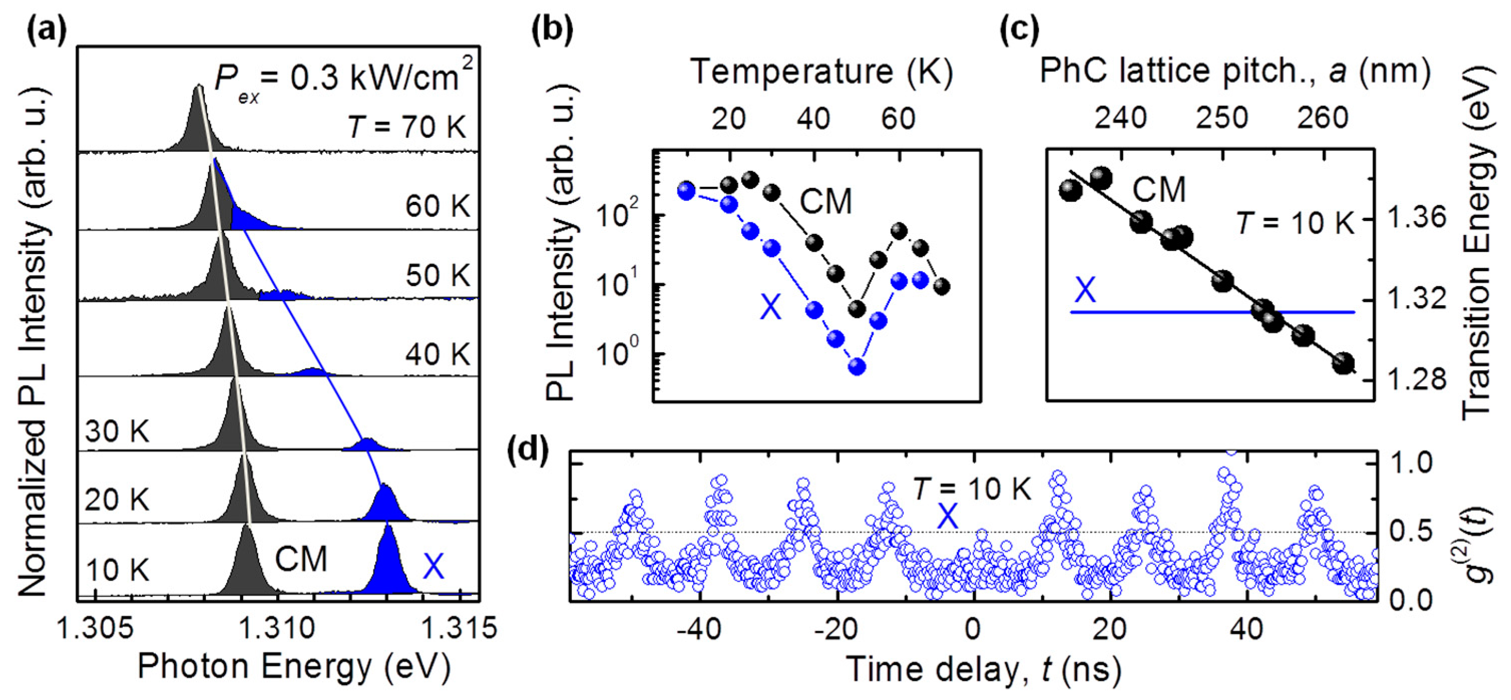
Table 1.
List of site-controlled QD fabrication-techniques suitable for integration in photonic devices. The techniques we developed (last two rows) are compared with those existing in the literature in terms of QD materials, position accuracy (Δx), and inhomogeneous broadening (ΔE).
Table 1.
List of site-controlled QD fabrication-techniques suitable for integration in photonic devices. The techniques we developed (last two rows) are compared with those existing in the literature in terms of QD materials, position accuracy (Δx), and inhomogeneous broadening (ΔE).
| Technique | QD Materials | Δx (nm) | ΔE (meV) |
|---|---|---|---|
| Inverted Pyramids [11] | InGaAs/GaAs | <50 | 1.4 |
| Pyramids [13,14] | InAs/InP | 50 | 50 |
| Nanoholes [16,17] | InAs/GaAs | 80 | 70 |
| Spatially selective H incorporation [28,29] | GaAsN/GaAs | 20 | 30 |
| Spatially selectiveH removal [30] | GaAsN/GaAs | <100 | 20 |
© 2018 by the authors. Licensee MDPI, Basel, Switzerland. This article is an open access article distributed under the terms and conditions of the Creative Commons Attribution (CC BY) license (http://creativecommons.org/licenses/by/4.0/).
Share and Cite
MDPI and ACS Style
Pettinari, G.; Felici, M.; Biccari, F.; Capizzi, M.; Polimeni, A. Site-Controlled Quantum Emitters in Dilute Nitrides and their Integration in Photonic Crystal Cavities. Photonics 2018, 5, 10. https://doi.org/10.3390/photonics5020010
AMA Style
Pettinari G, Felici M, Biccari F, Capizzi M, Polimeni A. Site-Controlled Quantum Emitters in Dilute Nitrides and their Integration in Photonic Crystal Cavities. Photonics. 2018; 5(2):10. https://doi.org/10.3390/photonics5020010
Chicago/Turabian StylePettinari, Giorgio, Marco Felici, Francesco Biccari, Mario Capizzi, and Antonio Polimeni. 2018. "Site-Controlled Quantum Emitters in Dilute Nitrides and their Integration in Photonic Crystal Cavities" Photonics 5, no. 2: 10. https://doi.org/10.3390/photonics5020010
Note that from the first issue of 2016, this journal uses article numbers instead of page numbers. See further details here.