Simulation of Photonic-Crystal Surface-Emitting Lasers with Air-Hole and Air-Pillar Structures


Institute of Electronics, National Yang Ming Chiao Tung University, Hsinchu City 30010, Taiwan
*
Author to whom correspondence should be addressed.
Photonics 2021, 8(6), 189; https://doi.org/10.3390/photonics8060189
Submission received: 29 April 2021
/
Revised: 26 May 2021
/
Accepted: 26 May 2021
/
Published: 27 May 2021
(This article belongs to the Special Issue Semiconductor Lasers)
Abstract
:Photonic-crystal surface-emitting lasers (PC-SELs), with and without regrowth, are theoretically simplified as air-hole and air-pillar structures, respectively. In this paper, square-latticed air-hole and air-pillar PC-SELs are simulated by a three-dimensional coupled-wave theory model and the design guideline is illustrated with a PC basis of a right isosceles triangular and double circular shapes. The optimum PC filling factor is determined by infinite PC cavity analysis and the slope efficiency of finite-size PC-SEL is then calculated for the lowest threshold band-edge mode. In comparison with air-hole PC-SEL, air-pillar PC-SEL exhibits lower threshold gain, larger gain discrimination but lower slope efficiency. To achieve slope efficiency of comparable value, the cavity area of air-pillar PC-SEL is about four times larger than that of air-hole PC-SEL.

1. Introduction
In 1999, photonic-crystal (PC) surface-emitting lasers (SELs), which exploit two-dimensional (2D) PC for both distributed feedback and surface emission, were demonstrated first on organic materials by Meier et al. [1] and then on semiconductor materials by Noda’s group [2]. Due to their large coherent emission area, PC-SELs have a small divergence angle (approaching diffraction limit [3]) and high output power (watt to ten-watt class [4,5]). With subtle changes of crystal basis, a large resonance area with high output power can maintain a single mode operation [5]. Moreover, PC-SELs are versatile; polarization [6,7], beam pattern [8,9] and beam direction [10,11] can be tailored by designing the unit cell structure properly. Recently, PC-SELs have drawn increasing attention due to their promising application to light detection and ranging (LiDAR) as well as laser processing [12,13].
There are at least three types of PC-SELs in terms of the fabrication scheme. The membrane-type PC-SELs were prepared by sacrificial etching to form a free-standing PC membrane [14]. However, mechanical weakness prevented it from further processing towards an electrical injection. The widely deployed scheme of embedded-type PC-SELs, where PC holes were buried within epitaxial layers by regrowth or wafer bonding, was proposed by Noda’s group [2,4]. The etched PC holes were placed adjacent to the active layers for efficient diffraction coupling. These air holes should be carefully retained without introducing additional defects during the burying step. Figure 1a shows its schematic structure and is referred to as air-hole PC-SEL. Alternatively, we have demonstrated the slab-type PC-SELs by directly depositing indium-tin-oxide (ITO) over the “PC slab-on-substrate” structure [15,16]. The ITO layer facilitated both electrical current spreading and optical light transmission. To maintain comparable diffraction coupling with practical technology, the thickness of the top cladding layer was greatly reduced and PC holes were deeply etched to form air pillars. Figure 1b shows its schematic structure and is referred to as air-pillar PC-SEL.
Air-pillar PC-SELs were simple in fabrication but critical in design. Experimental measurement and analysis revealed their low slope efficiency and weak feedback coupling as compared to air-hole PC-SELs [16]. Moreover, no three-dimensional (3D) simulation is carried out on air-pillar PC-SELs and device parameters are not optimized yet. In this paper, simulation based on 3D coupled-wave theory (CWT) model [17,18] is performed on air-pillar PC-SELs and comparison is made with air-hole PC-SELs.
2. Simulated Structures
Table 1 shows the reference structure of air-hole PC-SEL in [18] (p. 15951). It consists of three layers of InGaAs quantum well (QW) spaced by GaAs layers. The layer thickness and corresponding refractive index are replicated as listed. The investigated PCs are square-lattice air holes with lattice constant a = 295 nm and filling factor, f, defined as the fraction of the hole area in a unit cell. The average refractive index of a single PC layer is given by
where na and nb are refractive indices of air and background material, respectively. The dummy layer is used to model the evanescent field of a guided mode. The compared structure of air-pillar PC-SEL (shown in Table 2) is modified from the reference structure. The average indices of two PC layers consisting of GaAs and AlGaAs materials are nav1 and nav2, respectively. Unless otherwise specified, real refractive indices are assumed for all layers.
3. Methods and Results
A 3D CWT model treating the finite-size effects of square-lattice PC-SELs with an air-hole structure was previously developed by Noda’s group [18]. To make a quantitative comparison between air-hole and air-pillar PC-SELs, we chose their published layer structure as the reference and modified it for our air-pillar PC-SEL as shown in Table 1 and Table 2, respectively.
3.1. Vertical Mode Profile
Coupled-wave equations are formulated in terms of four basic waves that have identical vertical profile [17,18,19]. The vertical profile, Θ0(z), is the fundamental guided mode or the solution of a one-dimensional (1D) wave equation given by
where k0 is the free-space wavenumber, β is the propagation constant, and n(z) is the refractive index of the multilayer structure with average index in the PC layer(s). The transfer matrix method (TMM) is employed to solve Θ0(z) under the phase matching condition which satisfies
where β0 is the length of the reciprocal square lattice vector. We simulated the vertical intensity profile and calculated its one-dimensional (1D) confinement factor or intensity overlap within the QW and PC regions for both air-hole and air-pillar PC-SELs.
Figure 2a and Figure 3a show the normalized intensity as well as refractive index profile along the vertical direction at filling factor f = 0.16 for air-hole PC-SEL and air-pillar PC-SELs, respectively. In general, air-pillar PC-SEL suffered from asymmetric intensity distribution and lower peak intensity. The QW confinement factor of air-pillar PC-SEL is lower by 18% compared to air-hole PC-SEL. Moreover, the PC confinement factor of air-pillar PC-SEL is lower by 39% even though its thickness is over four times larger than air-hole PC-SEL. To go further, the confinement factor is calculated as a function of the PC filling factor. Figure 2b and Figure 3b reveal that the QW confinement versus the filling factor is monotonically increasing for air-hole PC-SEL but monotonically decreasing for air-pillar PC-SEL. The PC confinement decreases monotonically with filling factor for both air-hole PC-SEL and air-pillar PC-SEL; however, air-pillar PC-SEL shows a lower value and steeper decrease than air-hole PC-SEL.
3.2. Threshold Behavior of Infinite Cavity
The four basic waves in the coupled-wave equations (with vertical profile decoupled) are Rx, Sx, Ry and Sy, which represent their complex amplitudes propagating in the in-plane directions of +x, −x, +y and −y, respectively. In an infinite laser cavity, the four basic waves are independent of in-plane coordinates. Solving the system of coupled-wave equations is an eigenvalue problem. The mode wavelengths and modal losses (or threshold gains) can be obtained from the real part and imaginary part of the eigenvalues, respectively.
The PC basis of two different shapes are investigated in this paper. They are specially selected for their superior performance of high slope efficiency and single mode output [4,5]. One is a right isosceles triangular (RIT) design with side length of b as shown in Figure 4a. The other is a double circular (CC) design, shown in Figure 4b, with two circles allocated in a filling ratio of f1:f2 as well as separated in x and y directions by equal distance of Δ. For simplicity, we simulate air holes or pillars with perfectly straight (neither tapered nor tilted) sidewalls.
For infinite cavity with RIT design, the normalized frequencies of four band-edge modes A, B, C and D (named in decreasing wavelength) are calculated as a function of PC filling factor and shown in Figure 5a,b for air-hole and air-pillar PC-SELs, respectively. The corresponding modal power losses as a function of filling factor are shown in Figure 5c,d. There are at least three observations that can be addressed. First, air-hole PC-SEL shows smaller frequency values but larger variation ranges than air-pillar PC-SEL. This is due to the higher effective index and widely spread vertical mode profile of air-hole PC-SEL. Second, air-hole PC-SEL shows modal loss more than three times larger than air-pillar PC-SEL. This is ascribed to the larger diffraction coupling of air-hole PC-SEL. Besides, modes C and D suffer even more losses (in different scale) than modes A and B. Third, both air-hole and air-pillar PC-SELs show similar behavior; mode B is the lowest threshold mode, which switches to mode A at f ≈ 0.25.
For infinite cavity with CC design, we consider the specific filling ratio f1 = 3f2 and double-hole shift Δ = a/3. Figure 6a,b show the normalized frequencies of four band-edge modes as a function of filling factor for air-hole and air-pillar PC-SELs, respectively. The corresponding modal losses, as a function of filling factor, are shown in Figure 6c,d. As in the RIT design, the air-hole PC-SEL shows smaller frequency values but larger variation ranges than the air-pillar PC-SEL. Additionally, the air-hole PC-SEL shows modal loss more than three times larger than air-pillar PC-SEL. Different from the RIT design, the CC design exhibits four band-edge mode losses in a comparable scale. Moreover, mode A is the lowest threshold mode, which switches to mode D at f ≈ 0.2.
3.3. Finite Size Effect
In a finite-size square cavity with side length L, the four basic waves (Rx, Sx, Ry and Sy) are functions of the in-plane coordinates and discretized using a finite-difference method [20]. The system of coupled-wave equations is then solved by applying the non-reflecting boundary condition, i.e., Rx(0, y) = Sx(L, y) = Ry(x, 0) = Sy(x, L) = 0 [18,20].
For finite cavity with RIT design and f = 0.25, the total modal losses of the two lowest threshold fundamental band-edge modes (A0 and B0) are calculated and shown in Figure 7. The modal loss decreases rapidly with increasing cavity size because 2D optical feedback is built and in-plane loss drops dramatically in the large cavity size. The lowest threshold mode is A0 mode in our investigated range of cavity size. The modal losses of associated first high-order modes (A1 and B1) are also shown in Figure 7 to determine the threshold loss (or gain) discrimination, i.e., (). The maximum cavity sizes for stable single-mode operation (if gain discrimination over 10 cm−1 is required) are approximately 200 μm and 300 μm for air-hole and air-pillar PC-SELs, respectively.
The slope efficiency (SE) can be estimated according to the following formula
where λ0 is free-space wavelength in units of μm and αint is internal power loss with a typically assumed value of 5 cm−1. The factor 1/2 takes into account the fact that vertical radiation consists of both upward and downward components, and that only the upward-radiated component contributes to lasing output [4]. Since there is negligible (≈0) in-plane or edge power loss (αedge) in the infinite PC cavity, the total loss of individual mode is its surface radiation power loss (αrad). At the limit of the infinite cavity, the slope efficiencies of the lowest threshold modes can be calculated from Figure 5c,d; at f = 0.25, they are 0.61 W/A and 0.56 W/A for air-hole and air-pillar PC-SELs, respectively.
For finite cavity size, the in-plane and radiation losses can be resolved from the total losses [18] and slope efficiency is therefore calculated as shown in Figure 8. The lowest threshold mode is A0 mode, which exhibits higher slope efficiency than B0 mode. The horizontal dashed line is the upper limit set by the infinite cavity case. The slope efficiency of air-hole PC-SEL shows an initially rapid increase with cavity size compared to air-pillar PC-SEL.
For finite cavity with CC design and (f1, f2, Δ) = (0.15, 0.05, a/3), the modal power losses of the two lowest threshold fundamental modes (A0 and D0) as well as first high-order modes (A1 and D1) are calculated and shown in Figure 9a,b for air-hole and air-pillar PC-SELs, respectively. The lowest threshold mode is A0 mode in our investigated range of cavity size. The maximum cavity sizes for () over 10 cm−1 are about 200 μm and 300 μm for air-hole and air-pillar PC-SELs, respectively. However, the second lowest threshold mode is not A1 mode but D0 mode and the loss discrimination between A0 and D0 is only as small as 3 cm−1. Since the wavelength separation between A0 and D0 is over 3 nm, the loss discrimination between the fundamental mode and associated first high-order mode does matter. Nonetheless, it is better to separate the D0 mode by slightly decreasing the PC filling factor.
The slope efficiency for finite cavity size is calculated as shown in Figure 10. The lowest threshold, A0 mode, exhibits almost the same slope efficiency as the second lowest threshold, D0 mode. The horizontal dashed line is the upper limit set by the infinite cavity case. They are calculated from Figure 6c,d to be 0.6 W/A and 0.56 W/A for air-hole and air-pillar PC-SELs, respectively. The slope efficiency of air-hole PC-SEL also shows an initially rapid increase with cavity size compared to air-pillar PC-SEL. In contrast to RIT design, CC design exhibits a slightly smaller slope efficiency at the same cavity size.
3.4. Depth Effect
The radiation loss of air-hole PC-SEL was reported to change periodically with PC depth due to phase difference between radiation waves diffracted at different vertical positions within air holes [21]. We carried out the same investigation on the dependence of radiation loss against PC depth for air-hole and air-pillar PC-SELs as shown in Figure 11a,b, respectively. For infinite cavity with RIT design and f = 0.25, the lowest threshold mode of air-hole PC-SEL shows peak radiation loss at PC depth of 100 nm, which is around the thickness defined in Table 1. Moreover, the radiation loss in Figure 11a oscillates periodically as a function of PC depth with period of about 300 nm, which corresponds to the lattice constant or one-wavelength thickness. The oscillation of radiation loss was attributed to vertical interference between radiation waves from the top and bottom parts within the PC region [21].
Since the p-cladding thickness of air-pillar PC-SEL is fixed at 400 nm, the deeper PC depth is etched, the more diffraction PC couples with QW. Revisiting the vertical mode profiles in Section 3.1, one can tell the key difference between air-hole and air-pillar structures. The vertical mode profile of air-hole PC-SEL distributes across the bottom to the top of the PC region while that of the air-pillar PC-SEL penetrates only the bottom of the PC region. The vertical interference is thus absent or at least minimized for the air-pillar structure. Therefore, radiation loss increases monotonically with an increasing etched PC depth as shown in Figure 11b. Nonetheless, the maximum radiation loss of air-pillar PC-SEL is less than one third of that of air-hole PC-SEL.
4. Discussions
The 3D CWT model for air-hole PC-SEL was well developed by Noda’s group and its theoretical predictions of lowest threshold mode and beam profile were confirmed with experimental findings [18]. Moreover, their theory facilitates complicated analyses of device properties like slope efficiency, gain discrimination, non-uniform gain spatial distribution, etc. [18]. In contrast, our development of air-pillar PC-SEL is only at the initial stage and its device performance lags behind that of air-hole PC-SEL. In Section 3, the 3D CWT model is applied to the air-pillar structure and comparison is made between air-hole and air-pillar structures. Analyses of these simulation results provide valuable insights as follows.
First, the 1D intensity overlap revealed by the vertical mode profile can be a rough estimate of 2D diffraction coupling. The radiation loss of air-hole PC-SEL is more than three times larger than that of air-pillar PC-SEL even though their difference in PC confinement factor is as small as 3–4%. Moreover, the lower PC confinement factor of air-pillar PC-SEL contributes to lower diffraction coupling as observed in the experiments [15,16]. Second, the optimum filling factor for highest slope efficiency can be determined by infinite cavity analysis of Figure 5 and Figure 6. Analyzing radiation losses of band-edge modes against filling factor, the lowest threshold mode with either maximum radiation loss or mode switching is expected to have the highest slope efficiency. By the way, previous reports revealed the optimum filling factor for the lowest threshold [20,22]. There are no reports on what the optimum filling factor for highest efficiency is, to the best of our knowledge.
Third, finite cavity analysis of Figure 7 and Figure 9 reveals that air-pillar PC-SEL can achieve stable single-mode resonance over the emissions area about that is twice that of air-hole PC-SEL. The in-plane loss of air-pillar PC-SEL is greater than that of air-hole PC-SEL due to lower in-plane coupling caused by lower confinement factor in PC. As a result, the modal power loss of each mode become larger and the difference in modal loss between the two lowest modes becomes larger. Fourth, finite cavity analysis of Figure 8 and Figure 10 reveals that the required cavity area of air-pillar PC-SEL is about four times larger than that of air-hole PC-SEL in order to achieve slope efficiency of 90% of its respective upper limit. This is attributed to lower radiation loss but higher in-plane loss of air-pillar PC-SEL in comparison to air-hole PC-SEL.
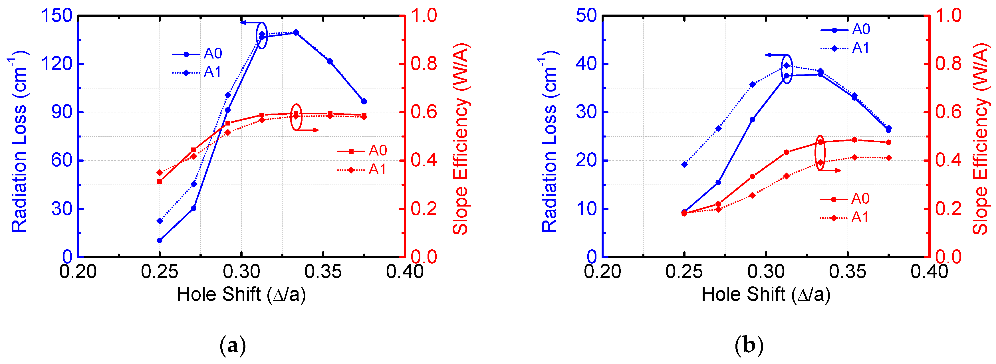
For the PC basis of CC design, we consider the double-hole shift Δ = a/3 instead of Δ = a/4 in [5] because of two experimental observations. First, Δ = a/4 is so close that two circles are frequently connected because of over exposure in e-beam lithography as well as enlarging in the deep etch of air pillars. Second, air-pillar PC-SELs with CC design and Δ = a/3 exhibit higher output efficiency than those with CC design and Δ = a/4. We calculated the radiation loss and slope efficiency of the lowest threshold mode (A0) and associated first high-order modes (A1) as a function of double-hole shift for air-hole and air-pillar PC-SELs as shown in Figure 12a,b, respectively.
As shown in Figure 12, the A0 mode of air-hole and air-pillar PC-SELs both show peak radiation loss at Δ = a/3 but peak slope efficiency at Δ = 0.354a for finite cavity size of 300 μm and CC design with (f1, f2, Δ) = (0.15, 0.05, a/3). In addition, the double-hole sizes are optimized around the filling ratio of 3:1. This is not shown here for simplicity and will be published later elsewhere. However, lower loss discrimination is paid for higher efficiency. The total (radiation and in-plane) loss discrimination is about 20 cm−1 at Δ = a/4 but less than 5 cm−1 at Δ = a/3 for air-hole PC-SEL. For air-pillar PC-SEL, the total loss discrimination is over 30 cm−1 at Δ = a/4 but about 12 cm−1 at Δ = a/3. To increase output efficiency around Δ = a/4, the authors in [5] chose a PC basis of a rotated elliptical shape instead of a circular shape. In a recent publication [23], Noda’s group incorporated the CC design with double-hole shift away from a quarter of lattice constant. They used (f1, f2, Δ) = (0.1, 0.03, 0.56a) to increase radiation loss [23] (p. 5053).
Regarding electrical and thermal conductance, we believe that air-pillar PC-SEL is inferior to air-hole PC-SEL. The air pillars reduce the semiconductor/ITO contact area where current is injected as well as where heat is dissipated; moreover, the electrical and thermal conductivity of ITO is poorer than that of GaAs where air holes are embedded. To improve the electrical and thermal properties, we propose to fabricate a substrate-emitting version of air-pillar PC-SEL. The window contact is replaced by a p-electrode which facilitates not only uniform current spreading but also die bonding on a thermally conductive submount.
5. Conclusions
We have simulated and compared PC-SELs with air-hole and air-pillar structures. Analysis of vertical mode profile reveals that air-hole PC-SEL exhibits larger intensity overlap within the PC region than air-pillar PC-SEL. The large intensity overlap results in enhanced diffraction coupling which contributes to large surface radiation loss. The optimum PC filling factor is therefore determined by analyzing modal losses of infinite PC cavity. For finite PC cavity, the modal loss decreases rapidly with increasing cavity size as 2D optical feedback is constructed and in-plane loss is greatly reduced. Compared to air-hole PC-SEL, air-pillar PC-SEL shows lower threshold gain and larger gain discrimination. A simple estimation reveals that air-pillar PC-SEL can achieve stable single-mode resonance over the emissions area twice as large as the air-hole PC-SEL. However, the lower radiation loss and higher in-plane loss of air-pillar PC-SEL results in its lower slope efficiency which can be compensated by the cavity area being four times larger than air-hole PC-SEL.
Author Contributions
Conceptualization, Z.-X.Y. and G.L.; Data curation, C.-Y.K.; Investigation, Z.-X.Y.; Software, Z.-X.Y.; Writing—original draft, Z.-X.Y. and G.L.; Writing—review & editing, G.L. All authors have read and agreed to the published version of the manuscript.
Funding
This research was funded by the Ministry of Science and Technology under grant number MOST 109-2218-E-009-022 and MOST 110-2218-E-A49-006.
Institutional Review Board Statement
Not applicable.
Informed Consent Statement
Informed consent was obtained from all subjects involved in this study.
Data Availability Statement
The data that support the findings of this study are available from the corresponding author upon reasonable request.
Acknowledgments
The authors would like to thank Chien-Ping Lee of National Yang Ming Chiao Tung University for valuable discussions.
Conflicts of Interest
The authors declare no conflict of interest.
References
- Meier, M.; Mekis, A.; Dodabalapur, A.; Timko, A.; Slusher, R.E.; Joannopoulos, J.D.; Nalamasu, O. Laser action from two-dimensional distributed feedback in photonic crystals. Appl. Phys. Lett. 1999, 74, 7–9. [Google Scholar] [CrossRef]
- Imada, M.; Noda, S.; Chutinan, A.; Tokuda, Y.; Murata, M.; Sasaki, G. Coherent two-dimensional lasing action in surface-emitting laser with triangular-lattice photonic crystal structure. Appl. Phys. Lett. 1999, 75, 316–318. [Google Scholar] [CrossRef]
- Riechel, S.; Kallinger, C.; Lemmer, U.; Feldmann, J.; Gombert, A.; Wittwer, V.; Scherf, U. A nearly diffraction limited surface emitting conjugated polymer laser utilizing a two-dimensional photonic band structure. Appl. Phys. Lett. 2000, 77, 2310–2312. [Google Scholar] [CrossRef]
- Hirose, K.; Liang, Y.; Kurosaka, Y.; Watanabe, A.; Sugiyama, T.; Noda, S. Watt-class high-power, high-beam-quality photonic-crystal lasers. Nat. Photonics 2014, 8, 406–411. [Google Scholar] [CrossRef]
- Yoshida, M.; De Zoysa, M.; Ishizaki, K.; Tanaka, Y.; Kawasaki, M.; Hatsuda, R.; Song, B.; Gelleta, J.; Noda, S. Double-lattice photonic-crystal resonators enabling high-brightness semiconductor lasers with symmetric narrow-divergence beams. Nat. Mater. 2019, 18, 121–128. [Google Scholar] [CrossRef] [PubMed]
- Noda, S.; Yokoyama, M.; Imada, M.; Chutinan, A.; Mochizuki, M. Polarization mode control of two-dimensional photonic crystal laser by unit cell structure design. Science 2001, 293, 1123–1125. [Google Scholar] [CrossRef] [PubMed]
- Mitsuru, Y.; Noda, S. Polarization mode control of two-dimensional photonic crystal laser having a square lattice structure. IEEE J. Quantum Electron. 2003, 39, 1074–1080. [Google Scholar]
- Miyai, E.; Sakai, K.; Okano, T.; Kunishi, W.; Ohnishi, D.; Noda, S. Lasers producing tailored beams. Nature 2006, 441, 946. [Google Scholar] [CrossRef] [PubMed]
- Kurosaka, Y.; Hirose, K.; Ito, A.; Hitaka, M.; Higuchi, A.; Sugiyama, T.; Takiguchi, Y.; Nomoto, Y.; Uenoyama, S.; Edamura, T. Beam pattern projecting on-chip lasers at visible wavelength. In Proceedings of the Conference on Lasers and Electro-Optics (CLEO): Science and Innovation, San Jose, CA, USA, 5–10 May 2019; p. SM4N.2. [Google Scholar]
- Sakata, R.; Ishizaki, K.; De Zoysa, M.; Fukuhara, S.; Inoue, T.; Tanaka, Y.; Iwata, K.; Hatsuda, R.; Yoshida, M.; Gelleta, J.; et al. Dually modulated photonic crystals enabling high-power high-beam-quality two-dimensional beam scanning lasers. Nat. Commun. 2020, 11, 3487. [Google Scholar] [CrossRef] [PubMed]
- Tanaka, Y.; Nishigo, A.; Kitamura, K.; Gelleta, J.; Noda, S. Modulated photonic-crystal surface-emitting laser with elliptical lattice points for two-dimensional coupling enhancement. AIP Adv. 2019, 9, 115204. [Google Scholar] [CrossRef]
- Noda, S. Progress of Photonic Crystal Surface-Emitting Lasers: Paradigm Shift for LiDAR Sensing and Laser Processing. In Proceedings of the SPIE 11672, Laser Resonators, Microresonators, and Beam Control XXIII, SPIE Photonics West, San Francisco, CA, USA, 6–11 March 2021. [Google Scholar]
- Noda, S.; Yoshida, M.; Kunishi, W.; Inoue, T.; Ishizaki, K.; De Zoysa, M.; Kitamura, K.; Shimaji, N.; Nishimura, K. Photonic crystal lasers: Fabrication with AI-assisted technology and application to LiDAR system. In Proceedings of the SPIE 11703, AI and Optical Data Sciences II, SPIE Photonics West, San Francisco, CA, USA, 6–11 March 2021. [Google Scholar]
- Kim, D.U.; Kim, S.; Lee, J.; Jeon, S.R.; Jeon, H. Free-standing GaN based photonic crystal band-edge laser. IEEE Photonics Technol. Lett. 2011, 23, 1454–1456. [Google Scholar] [CrossRef]
- Hsu, M.Y.; Lin, G.; Pan, C.H. Electrically injected 1.3-μm quantum-dot photonic-crystal surface- emitting lasers. Opt. Express 2018, 25, 32697–32704. [Google Scholar] [CrossRef]
- Hsu, M.Y.; Lin, G.; Li, Z.L.; Pan, P.C. Threshold current temperature dependence of quantum-dot photonic crystal surface-emitting lasers with respect to gain-cavity detuning. Opt. Express 2018, 26, 13483–13488. [Google Scholar] [CrossRef] [PubMed]
- Liang, Y.; Peng, C.; Sakai, K.; Iwahashi, S.; Noda, S. Three-dimensional coupled-wave model for square-lattice photonic crystal lasers with transverse electric polarization: A general approach. Phys. Rev. B 2011, 84, 195119. [Google Scholar] [CrossRef] [Green Version]
- Liang, Y.; Peng, C.; Sakai, K.; Iwahashi, S.; Noda, S. Three-dimensional coupled-wave analysis for square-lattice photonic crystal surface emitting lasers with transverse-electric polarization: Finite-size effects. Opt. Express 2012, 20, 15945–15961. [Google Scholar] [CrossRef] [PubMed]
- Peng, C.; Liang, Y.; Sakai, K.; Iwahashi, S.; Noda, S. Coupled-wave analysis for photonic-crystal surface-emitting lasers on air holes with arbitrary sidewalls. Opt. Express 2011, 19, 24672–24686. [Google Scholar] [CrossRef] [PubMed]
- Sakai, K.; Miyai, E.; Noda, S. Coupled-wave theory for square-lattice photonic crystal lasers with TE polarization. IEEE J. Quantum Electron. 2010, 46, 788–795. [Google Scholar] [CrossRef] [Green Version]
- Iwahashi, S.; Sakai, K.; Kurosaka, Y.; Noda, S. Air-hole design in a vertical direction for high-power two-dimensional photonic-crystal surface-emitting lasers. J. Opt. Soc. Am. B 2010, 27, 1204–1207. [Google Scholar] [CrossRef]
- Hung, C.T.; Syu, Y.C.; Wu, T.T.; Lu, T.C. Design of Low-Threshold Photonic Crystal Surface-Emitting Lasers. IEEE Photonics Technol. Lett. 2012, 24, 866–868. [Google Scholar] [CrossRef]
- Inoue, T.; Yoshida, M.; De Zoysa, M.; Ishizaki, K.; Noda, S. Design of photonic-crystal surface-emitting lasers with enhanced in-plane optical feedback for high-speed operation. Opt. Express 2020, 28, 5050–5057. [Google Scholar] [CrossRef]
Figure 1.
The schematic structures of (a) air-hole PC-SEL and (b) air-pillar PC-SEL under investigation.
Figure 1.
The schematic structures of (a) air-hole PC-SEL and (b) air-pillar PC-SEL under investigation.
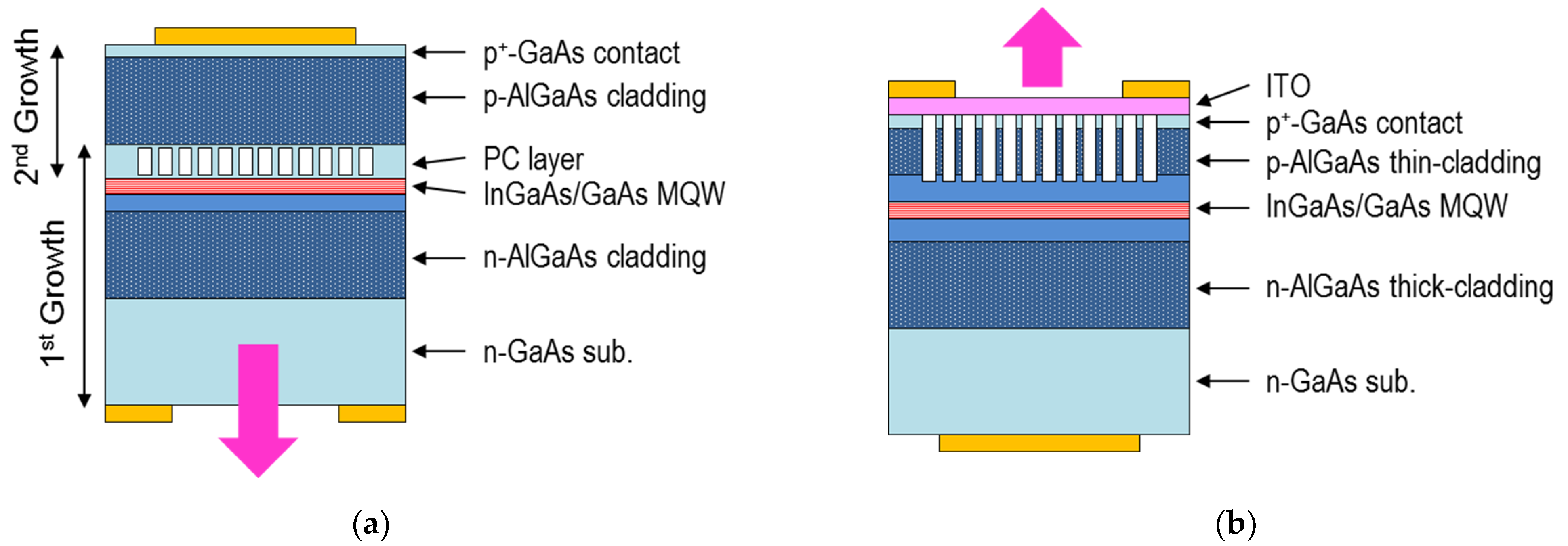
Figure 2.
Air-hole PC-SEL: (a) the normalized intensity as well as refractive index profile at filling factor f = 0.16 (b) the 1D intensity overlap within QW and PC regions as a function of PC filling factor.
Figure 2.
Air-hole PC-SEL: (a) the normalized intensity as well as refractive index profile at filling factor f = 0.16 (b) the 1D intensity overlap within QW and PC regions as a function of PC filling factor.

Figure 3.
Air-pillar PC-SEL: (a) the normalized intensity as well as refractive index profile at filling factor f = 0.16 (b) the 1D intensity overlap within QW and PC regions as a function of PC filling factor.
Figure 3.
Air-pillar PC-SEL: (a) the normalized intensity as well as refractive index profile at filling factor f = 0.16 (b) the 1D intensity overlap within QW and PC regions as a function of PC filling factor.
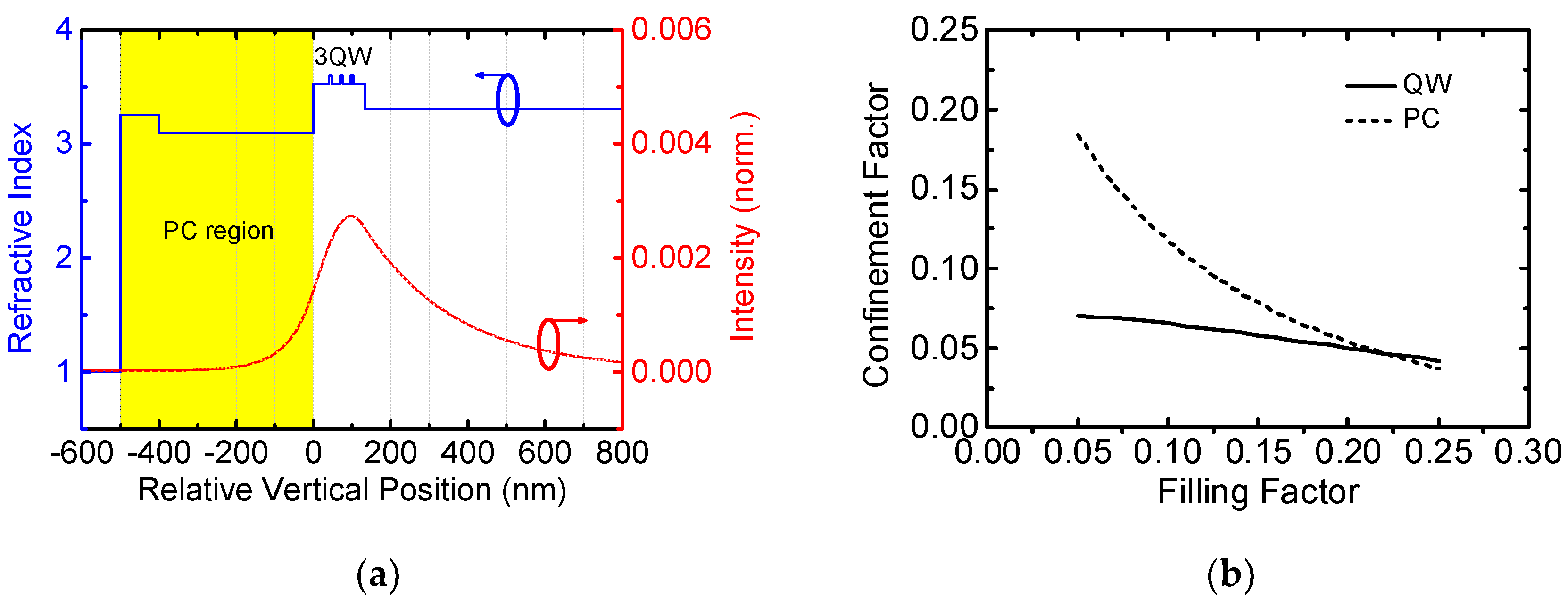
Figure 4.
The investigated unit cells with (a) RIT and (b) CC shaped bases.
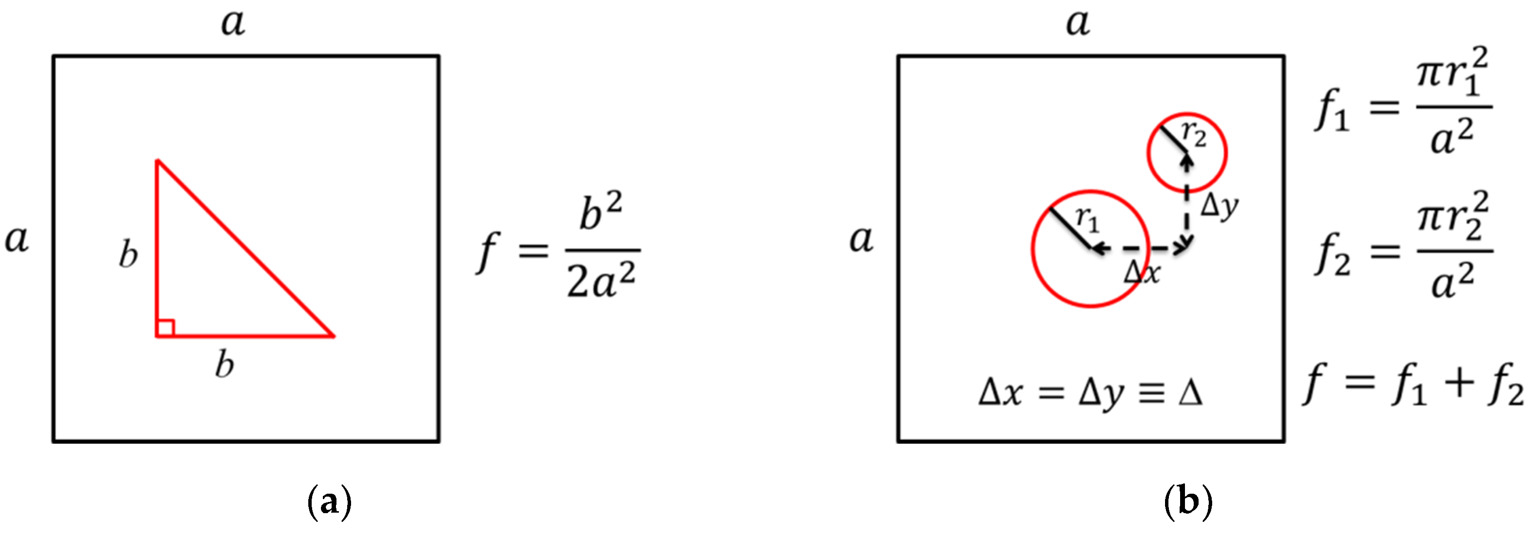
Figure 5.
Infinite cavity with RIT design: the normalized frequencies of four band-edge modes versus filling factor for (a) air-hole and (b) air-pillar PC-SELs; the modal power losses of four band-edge modes versus filling factor for (c) air-hole and (d) air-pillar PC-SELs.
Figure 5.
Infinite cavity with RIT design: the normalized frequencies of four band-edge modes versus filling factor for (a) air-hole and (b) air-pillar PC-SELs; the modal power losses of four band-edge modes versus filling factor for (c) air-hole and (d) air-pillar PC-SELs.
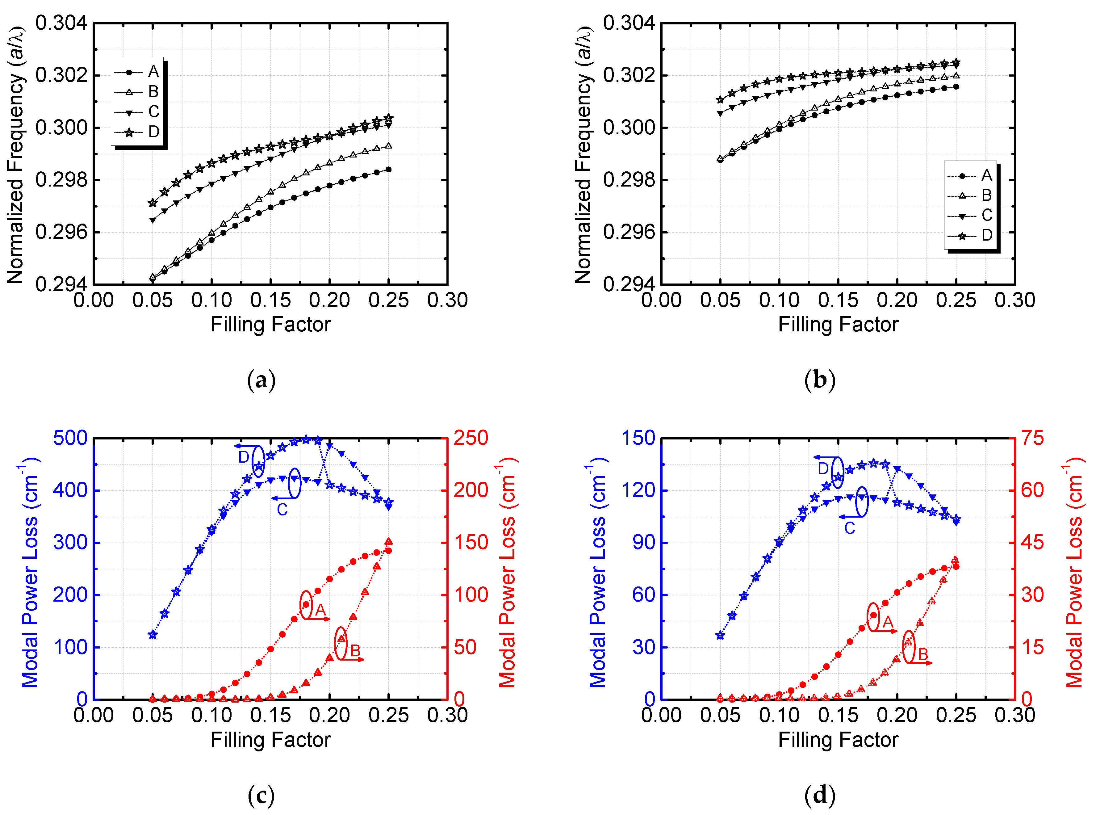
Figure 6.
Infinite cavity with CC design (f1 = 3f2, Δ = a/3): the normalized frequencies of four band-edge modes versus filling factor for (a) air-hole and (b) air-pillar PC-SELs; the modal power losses of four band-edge modes versus filling factor for (c) air-hole and (d) air-pillar PC-SELs.
Figure 6.
Infinite cavity with CC design (f1 = 3f2, Δ = a/3): the normalized frequencies of four band-edge modes versus filling factor for (a) air-hole and (b) air-pillar PC-SELs; the modal power losses of four band-edge modes versus filling factor for (c) air-hole and (d) air-pillar PC-SELs.

Figure 7.
Finite cavity with RIT design (f = 0.25): the total modal losses of the two lowest fundamental modes as well as associated first high-order modes as a function of PC cavity size for (a) air-hole and (b) air-pillar PC-SELs.
Figure 7.
Finite cavity with RIT design (f = 0.25): the total modal losses of the two lowest fundamental modes as well as associated first high-order modes as a function of PC cavity size for (a) air-hole and (b) air-pillar PC-SELs.

Figure 8.
Finite cavity with RIT design (f = 0.25): the slope efficiency of the two lowest threshold fundamental modes as a function of PC cavity size for (a) air-hole and (b) air-pillar PC-SELs.
Figure 8.
Finite cavity with RIT design (f = 0.25): the slope efficiency of the two lowest threshold fundamental modes as a function of PC cavity size for (a) air-hole and (b) air-pillar PC-SELs.
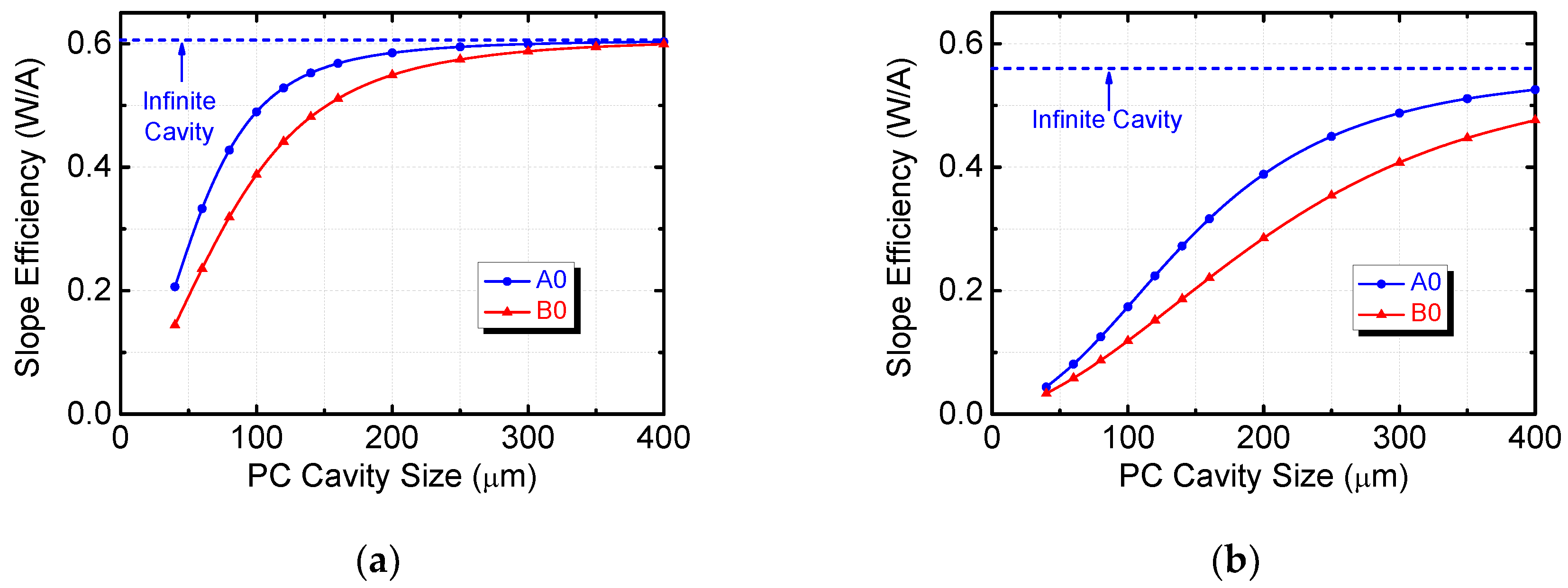
Figure 9.
Finite cavity with CC design (f1, f2, Δ) = (0.15, 0.05, a/3): the total modal losses of the two lowest fundamental modes as well as associated first high-order modes as a function of PC cavity size for (a) air-hole and (b) air-pillar PC-SELs.
Figure 9.
Finite cavity with CC design (f1, f2, Δ) = (0.15, 0.05, a/3): the total modal losses of the two lowest fundamental modes as well as associated first high-order modes as a function of PC cavity size for (a) air-hole and (b) air-pillar PC-SELs.
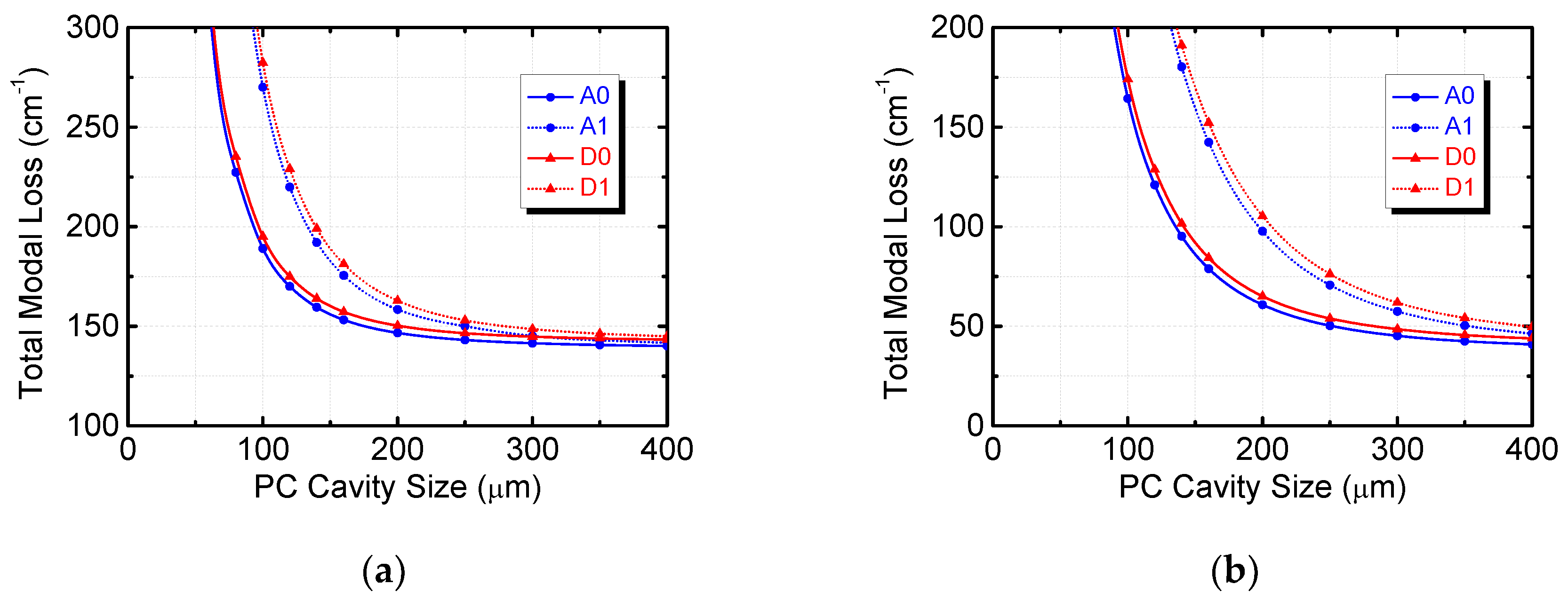
Figure 10.
Finite cavity with CC design (f1, f2, Δ) = (0.15, 0.05, a/3): the slope efficiency of the two lowest fundamental modes as a function of PC cavity size for (a) air-hole and (b) air-pillar PC-SELs.
Figure 10.
Finite cavity with CC design (f1, f2, Δ) = (0.15, 0.05, a/3): the slope efficiency of the two lowest fundamental modes as a function of PC cavity size for (a) air-hole and (b) air-pillar PC-SELs.
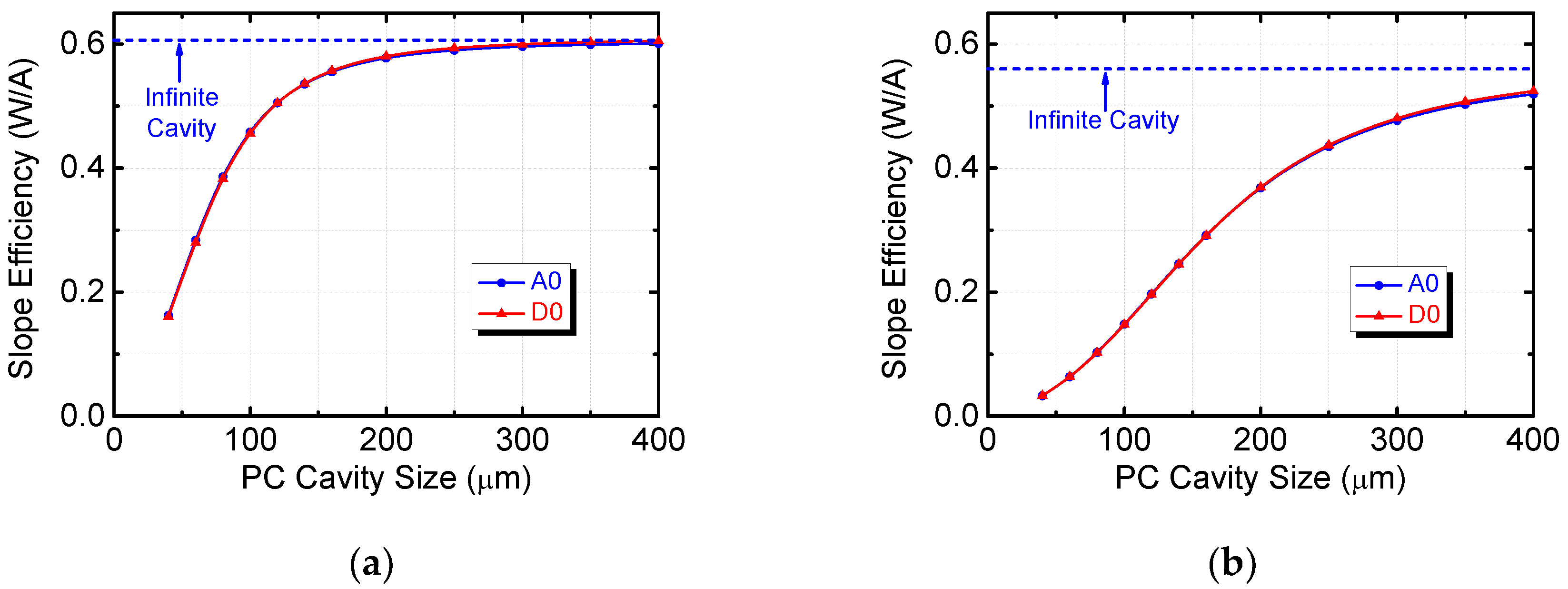
Figure 11.
The radiation loss is investigated in terms of PC depth for (a) air-hole and (b) air-pillar PC-SELs assuming infinite cavity and RIT design with f = 0.25.
Figure 11.
The radiation loss is investigated in terms of PC depth for (a) air-hole and (b) air-pillar PC-SELs assuming infinite cavity and RIT design with f = 0.25.

Figure 12.
The radiation loss and slope efficiency of the lowest threshold mode and associated first high-order modes as a function of double-hole shift for (a) air-hole and (b) air-pillar PC-SELs assuming finite cavity size of 300 μm and CC design with (f1, f2, Δ) = (0.15, 0.05, a/3).
Figure 12.
The radiation loss and slope efficiency of the lowest threshold mode and associated first high-order modes as a function of double-hole shift for (a) air-hole and (b) air-pillar PC-SELs assuming finite cavity size of 300 μm and CC design with (f1, f2, Δ) = (0.15, 0.05, a/3).

Table 1.
The simulated layer structure of air-hole PC-SEL [18].
Table 1.
The simulated layer structure of air-hole PC-SEL [18].
| Layer Description | Thickness (nm) | Refractive Index [18] |
|---|---|---|
| Dummy | - | 1.0 |
| p-contact (GaAs) | 100 | 3.524 |
| p-cladding (AlGaAs) | 1500 | 3.307 |
| GaAs | 20 | 3.524 |
| GaAs + PC (Air Hole) | 118 | nav (3.524 & 1.0) |
| GaAs | 22 | 3.524 |
| cladding (AlGaAs) | 40 | 3.279 |
| GaAs spacer | 40 | 3.524 |
| 3QW (InGaAs/GaAs) | 8 × 3/20 × 2 | 3.6/3.524 |
| GaAs spacer | 30 | 3.524 |
| n-cladding (AlGaAs) | 1500 | 3.307 |
Table 2.
The simulated layer structure of air-pillar PC-SEL.
| Layer Description | Thickness (nm) | Refractive Index |
|---|---|---|
| Dummy | - | 1.0 |
| p-contact (GaAs) + PC1 (Air Pillar) | 100 | nav1 (3.524 & 1.0) |
| p-cladding (AlGaAs) + PC2 (Air Pillar) | 400 | nav2 (3.307 & 1.0) |
| GaAs spacer | 40 | 3.524 |
| 3QW (InGaAs/GaAs) | 8 × 3/20 × 2 | 3.6/3.524 |
| GaAs spacer | 30 | 3.524 |
| n-cladding (AlGaAs) | 1500 | 3.307 |
Publisher’s Note: MDPI stays neutral with regard to jurisdictional claims in published maps and institutional affiliations. |
© 2021 by the authors. Licensee MDPI, Basel, Switzerland. This article is an open access article distributed under the terms and conditions of the Creative Commons Attribution (CC BY) license (https://creativecommons.org/licenses/by/4.0/).
Share and Cite
MDPI and ACS Style
Yang, Z.-X.; Kuo, C.-Y.; Lin, G. Simulation of Photonic-Crystal Surface-Emitting Lasers with Air-Hole and Air-Pillar Structures. Photonics 2021, 8, 189. https://doi.org/10.3390/photonics8060189
AMA Style
Yang Z-X, Kuo C-Y, Lin G. Simulation of Photonic-Crystal Surface-Emitting Lasers with Air-Hole and Air-Pillar Structures. Photonics. 2021; 8(6):189. https://doi.org/10.3390/photonics8060189
Chicago/Turabian StyleYang, Zi-Xian, Chia-Yu Kuo, and Gray Lin. 2021. "Simulation of Photonic-Crystal Surface-Emitting Lasers with Air-Hole and Air-Pillar Structures" Photonics 8, no. 6: 189. https://doi.org/10.3390/photonics8060189
Note that from the first issue of 2016, this journal uses article numbers instead of page numbers. See further details here.