Communication

Interlayer Slope Waveguide Coupler for Multilayer Chalcogenide Photonics

1
College of Optical Science and Engineering, Zhejiang University, Hangzhou 310027, China
2
Key Laboratory of 3D Micro/Nano Fabrication and Characterization of Zhejiang Province, School of Engineering, Westlake University, Hangzhou 310024, China
3
Institute of Advanced Technology, Westlake Institute for Advanced Study, Hangzhou 310024, China
4
State Key Laboratory of Modern Optical Instrumentation, College of Information Science and Electronic Engineering, Zhejiang University, Hangzhou 310027, China
5
The College of Optics & Photonics, Department of Materials Science & Engineering, University of Central Florida, Orlando, FL 32816, USA
*
Author to whom correspondence should be addressed.
Photonics 2022, 9(2), 94; https://doi.org/10.3390/photonics9020094
Submission received: 18 January 2022 / Revised: 29 January 2022 / Accepted: 30 January 2022 / Published: 7 February 2022
(This article belongs to the Special Issue Glass Optics)

Abstract

:
The interlayer coupler is one of the critical building blocks for optical interconnect based on multilayer photonic integration to realize light coupling between stacked optical waveguides. However, commonly used coupling strategies, such as evanescent field coupling, usually require a close distance, which could cause undesired interlayer crosstalk. This work presents a novel interlayer slope waveguide coupler based on a multilayer chalcogenide glass photonic platform, enabling light to be directly guided from one layer to another with a large interlayer gap (1 µm), a small footprint (6 × 1 × 0.8 µm3), low propagation loss (0.2 dB at 1520 nm), low device processing temperature, and a high bandwidth, similar to that in a straight waveguide. The proposed interlayer slope waveguide coupler could further promote the development of advanced multilayer integration in 3D optical communications systems.

1. Introduction

The exponential growth in data communications and computing requires scalable, high-yield, and cost-effective integrated photonic systems. In recent years, large-scale and high-density multilayer photonic integrated circuits (PICs) with higher integration have developed rapidly, due to their new functionality and high energy efficiency [1,2,3,4,5,6,7]. Silicon (Si) photonics could be a suitable integration platform due to its unique complementary metal-oxide-semiconductor (CMOS) compatibility, but challenges in stacking up single crystal silicon layers impede the development of stacked multilayer silicon photonics [8]. In addition, the hybrid integration of silicon with other materials (such as silicon nitride [9,10], amorphous silicon [11,12], and polycrystalline silicon [13]) suffer from complexities in fabrication, such as the requirements of high-temperature deposition for low-loss thin films, chemical-mechanical polishing for planarizing the structures, and the wafer-bonding process for heterogeneous integration. In contrast, chalcogenide glasses (ChGs) are amorphous inorganic materials with unique properties such as infrared transparency, high nonlinearity, and a high refractive index. Their amorphous nature enables them to be both monolithically and heterogeneously integrated with a wide variety of materials at a low deposition temperature, compatible with the COMS back-end process. These remarkable material properties make them a viable platform for future multilayer optical communications systems [14,15,16,17,18,19,20,21,22,23], mid-infrared integrated photonic devices [22,24,25], sensors [26,27,28] and flexible photonic devices [29,30,31,32].
One of the main challenges of multilayer technology lies in coupling light between layers. Current coupling schemes include evanescent couplers, grating couplers, and direct 3D waveguide coupling. The high-efficiency evanescent coupler [2,33,34,35,36,37,38] usually requires a close distance and a large footprint, inducing a lower integration density and more serious interlayer crosstalk, respectively. Grating couplers [8,39,40] are highly sensitive to wavelength and light polarization, which imposes severe bandwidth limitations on their coupling performance. Moreover, multiple diffracted orders of grating couplers, when coupled into waveguides in other layers, could lead to crosstalk or other undesirable interactions. Thus, higher demands on the design of high-performance, compact, high-density optical routing strategies are necessary. The 3D waveguide design [12], using an interlayer slope waveguide coupler to directly connect the waveguides in different layers, allows a more considerable interlayer distance, a higher coupling efficiency, and a smaller footprint, thus making it more suitable for high-density multilayer integration.
Here, we report on an interlayer 3D slope waveguide coupler fabricated using ChG material at low temperatures and even close to room temperature. We theoretically analyzed the mode conversion between straight and interlayer slope waveguides for different slope angles. The interlayer gap and the slope angle were designed to be 1 µm and 10° to optimize the transmission efficiency and avoid interlayer crosstalk. The Ge23Sb7S70 (GSS) interlayer slope waveguide coupler with 800 nm width and 450 nm height was designed to only support the fundamental mode. By adjusting the photoresist adhesion, we can flexibly control the angle of the interlayer slope waveguide coupler. The fabricated interlayer slope waveguide coupler shows an insertion loss of 0.2 dB at 1520 nm for the transverse electrical (TE) mode. Unlike an interlayer grating coupler and an evanescent coupler, the interlayer slope waveguide coupler has an ultra-large bandwidth similar to that of a straight waveguide.

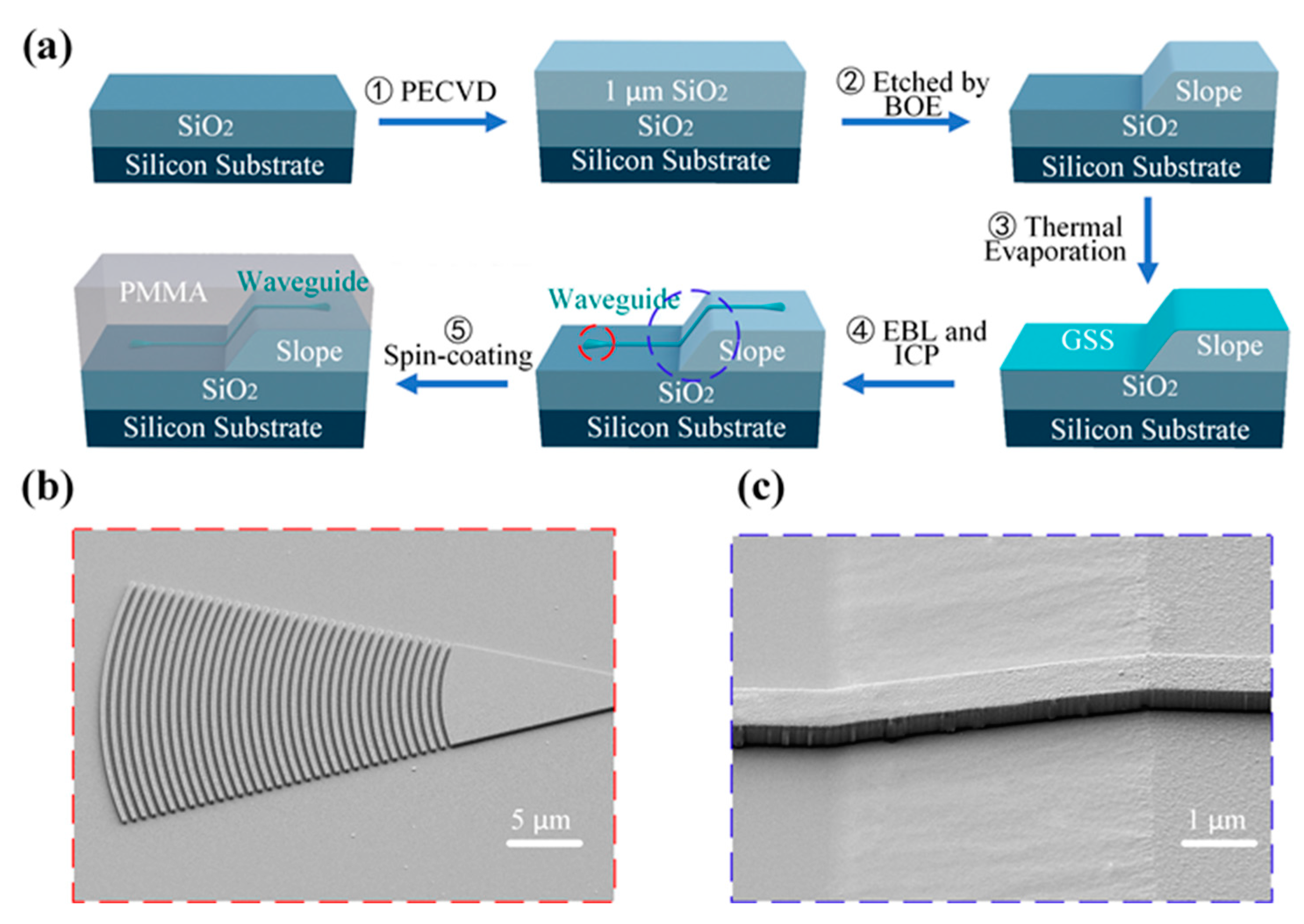
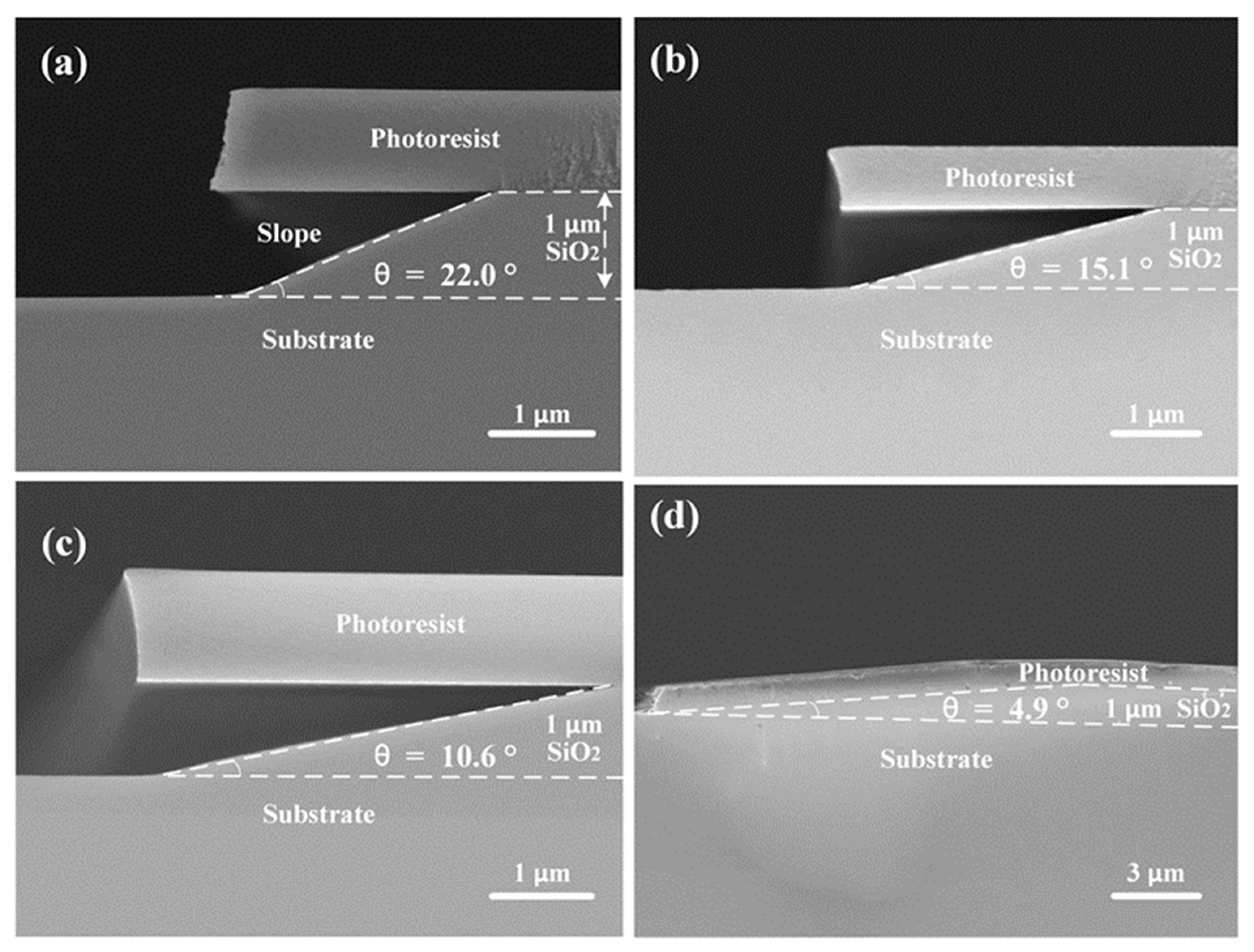
2. Design and Fabrication

We designed and optimized the structure of the interlayer waveguide coupler by 3D Finite Difference Time Domain (FDTD) simulation. Figure 1a shows the schematic diagram of the interlayer slope waveguide coupler based on the ChG platform. Due to its superior chemical and physical stability [41] and low loss in the S + C + L band [42], GSS was adopted as the waveguide core material. The refractive index of GSS was 2.26 at 1520 nm. The waveguide had a width (w2) of 800 nm and a height (h2) of 450 nm, which only supported the fundamental mode. The height of the interlayer slope (h1) was set as 1 µm to avoid interlayer crosstalk. The coupling efficiency of the interlayer slope waveguide coupler with different slope angles θ was calculated by 3D FDTD at 1520 nm for TE0 mode, as shown in Figure 1b. As the slope angle increases, the slope length decreases, and the loss gradually increases. When the slope angle was 5–20°, the transmission loss of a single slope waveguide was below 0.36 dB. When the slope angle was 40°, the transmission loss of the slope waveguide sharply increased to 3.51 dB.
The insertion loss of the interlayer waveguide was analyzed by coupling mode theory [43]. Figure 1c shows the electric field transmission in the interlayer slope waveguide coupler with a slope angle of 10° at 1520 nm corresponding to the red dotted circle in Figure 1b. The input port is at the bottom layer, and the output is at the top layer. The straight waveguide’s effective refractive index (neff) calculated by 3D FDTD was 1.849, while the neff of the interlayer slope waveguide at 10° was around 1.852. The light from the straight waveguide encountered a slight mode mismatch, causing a slight insertion loss of 0.14 dB. Most light was confined to the waveguides as they passed through the interlayer slope waveguide, supporting only the fundamental mode. Figure 1d shows the electric field transmission in the interlayer slope waveguide with a slope angle of 40°, corresponding to the blue dotted circle in Figure 1b. The straight waveguide’s neff was also around 1.849, while the neff of the slope waveguide at 40° was around 1.922. The light from the straight waveguide encountered a more considerable mode mismatch, causing an insertion loss of 3.51 dB. After passing through the slope waveguide, only 45% of the energy could be transmitted from the bottom to the top. A smaller slope angle introduced lower loss but resulted in a larger footprint. Therefore, there was a tradeoff between device size and insertion loss. Here, we chose an interlayer slope waveguide with an angle of 10° to achieve both small size and low insertion loss.
The device fabrication was carried out at the Westlake Center for Micro/Nano Fabrication and the ZJU Micro-Nano Fabrication Center. Figure 2a shows the fabrication process flow of the interlayer slope GSS waveguide coupler. Firstly, 1-µm-thick silicon oxide was deposited on a commercial 4-inch silicon wafer with a 2 µm thickness oxide layer by plasma-enhanced chemical vapor deposition (PECVD, manufactured by Samco Inc., Kyoto, Japan). The photoresist (NR9 1500PY) was spin-coated onto the wafer and patterned by optical lithography (ABM Mask Aligner). The sample was immersed in buffered oxide etch solution (BOE, HF: NH4F = 15:2); the etching rate was 200 nm/min. At the edge of the photoresist area, the lateral etching of BOE induced a fixed angle slope [44]. The photoresist on the sample surface was removed by soaking in acetone for 2 h, followed by O2 plasma treatment for around 3 min to completely remove the residual organic material on the sample. A 450-nm-thick GSS film was deposited on the sample by thermal evaporation at room temperature, and a layer of 50-nm thick silicon oxide was sputtered onto its surface, which can prevent the etching of GSS material by the alkaline solution. The electron beam lithography photoresist (maN 2403) was spin-coated on the sample, and the device pattern was patterned by electron beam exposure (EBL, manufactured by Raith Inc., Dortmund, Germany). The sample was then etched by inductively coupled plasma (ICP, manufactured by Leuven Inc., Xuzhou, China) using a fluorine-based atmosphere (CF4:CHF3 = 1:3) with a selective etching ratio of 1:4 and an etching rate of 40 nm/s. An appropriate oxygen plasma recipe can remove the residual photoresist on the surface of the device. Figure 2b shows the scanning electron microscope (SEM) image of the focusing grating coupler on the bottom layer with a period of 0.97 µm and a duty cycle of 0.5. Figure 2c shows the SEM image of the interlayer slope GSS waveguide coupler with a slope length of 5.6 µm (slope angle of 10.6°) and a waveguide width of 800 nm. Finally, a 2-µm thick PMMA was spin-coated onto the sample as the top cladding layer.
The angle of the interlayer waveguide was controlled by adjusting the adhesion of the photoresist to the substrate. A lower bake temperature could cause poorer adhesion, resulting in the slope with a smaller angle, as shown in Figure 3 [12]. The photoresist would collapse onto the substrate at a slope angle of 4.9° due to the relatively long slope length shown in Figure 3d. Table 1 shows the slope angles for four samples at different bake temperatures after a wet etching in BOE for five minutes. In the following measurement section, the test sample was fabricated on sample C with a slope angle of 10.6° and a slope length of 5.6 µm.

3. Results and Discussion

A broadband tunable laser system (TSL 550, manufactured by Santec Inc., Komaki, Japan) was used to characterize the fabricated devices. The light launched from the tunable laser was adjusted by the polarization rotator (PR) and coupled into the chip through a vertical coupling system. In order to minimize the transmittance error of the slope waveguide, estimated to be less than 10%, six test devices with different slope numbers were fabricated on the same chip, as shown in Figure 4a. A straight waveguide of 300 µm was used to connect the two adjacent interlayer slope waveguide couplers. The right inset in Figure 4a shows the SEM image of the interlayer slope waveguide coupler, with a slope height of 1 µm and a slope length of 5.6 µm (slope angle of 10.6°). The transmission spectra of six test devices were measured separately. The insertion loss of the focusing grating coupler was around 5 dB at 1520 nm. The insertion loss per cell consisting of an interlayer slope waveguide coupler and a 300 µm straight waveguide in the wavelength range between 1400–1580 nm was calculated by linear fitting, as shown in Figure 4b. The insertion loss per segment was around 0.8 dB in the wavelength range between 1400–1580 nm (limited by the transmission spectrum of the focusing grating coupler). The inset in Figure 4b shows the linear fitting of the insertion loss at 1520 nm.
A microring resonator (MRR) was designed and fabricated on the same chip to calculate the waveguide’s transmission loss at the bottom and top layers, as shown in the insets of Figure 4c,d. The transmission spectrum of the MRR is shown in Figure 4c,d and fitted using the Lorentz function [45,46]. The loaded quality factor (Q) could be calculated by Q L = λ r Δ λ , where λ r denotes the resonant wavelength and Δ λ represents the full width at half maximum (FWHM) of the dip in the transmission spectrum. The intrinsic Q is calculated by
Q i = 2 Q L 1 ± R
where R denotes the on-resonance fraction of optical power reflected by the cavity and is calculated by the dip’s extinction ratio (ER), and ± corresponds to the under- and over- coupled loading condition [47,48]. The intrinsic Q value is 1.2 × 10⁴. The waveguide transmission loss α (in cm−1) is calculated by
α = 2 π n g Q i λ r
where n g represents the group index inferred from the free spectral range (FSR).
n g = λ r 2 L × F S R
were L is the round-trip length of the resonator. Equation (2) gives a waveguide propagation loss of 19.7 dB/cm for the waveguide on the top and bottom layer. Thus the insertion loss of one interlayer slope waveguide coupler is around 0.2 dB, which is slightly larger than that obtained by simulation calculation due to the roughness on the sidewall of the slope waveguide.
To investigate the source of light propagation loss in the waveguide, we measured the surface roughness of the top, bottom, and interlayer slopes using an atomic force microscope (AFM, Bruker Corporation, Billerica, MA, USA). The root-mean-square (RMS) of surface roughness was 1.24 nm, 0.35 nm, and 0.30 nm on the top, interlayer slope, and bottom layer, respectively, as shown in Figure 5b–d. In addition, the sidewall of the straight waveguide has a significant degree of line-edge roughness, which can be found from SEM in Figure 2c. Thus, smoothing the slope connection and decreasing the sidewall and surface roughness by optimizing the fabrication process could further reduce the waveguide propagation loss.
To highlight the role of material choice, component geometry and performance, we compared the figures of merit in terms of optical performance and dimension with different interlayer couplers in Table 2. The grating couplers have a relatively narrow bandwidth, large footprint, and high insertion loss. The tri-layer crossing requires a complex fabrication process. The double-layer waveguide evanescent couplers require a close interlayer gap (700 nm) and a large footprint, usually exhibiting high interlayer crosstalk. A meta-structure-based interlayer directional coupler enables the interlayer gap to be increased to 1.4 µm to suppress the interlayer coupling; however, there is a high insertion loss that needs to be considered. The interlayer slope waveguide coupler fabricated by Si:H allows a more considerable interlayer distance, a higher coupling efficiency, and a smaller footprint, while the low device processing temperature of GSS is more compatible for the Back End of Line (BEOL) process.
Our results demonstrate the ability to design and fabricate a superior coupling device scheme that does not suffer from limitations defined for other strategies previously reported, allowing for multiple preferred device conditions simultaneously. These enhancements demonstrate flexibility in fabrication that can result in a large interlayer gap, a small footprint, low propagation loss, low device processing temperature, and a high bandwidth similar to that in a straight waveguide. Such tailorability and simultaneous performance superiority will enable flexibility in a variety of designs.

4. Conclusions

In summary, we fabricated an interlayer slope waveguide coupler for multilayer photonic integration based on the room-temperature-deposited GSS platform. The 3D interlayer slope waveguide coupler directly transfers the light within the different layers with negligible loss and interlayer crosstalk. The angle of the interlayer slope waveguide coupler can be flexibly controlled by adjusting the adhesion of the photoresist to the substrate. The fabricated interlayer slope waveguide coupler shows an insertion loss of 0.2 dB at 1520 nm for the transverse electrical (TE) mode. The interlayer slope waveguide coupler had an ultra-large bandwidth similar to that in a straight waveguide. The fabricated interlayer gap was 1 µm, the slope angle was 10.6°. A small footprint of 6 × 1 × 0.8 µm3 of the interlayer coupler was demonstrated. The source of insertion loss could be reduced by optimizing the fabrication process and improving the surface and sidewall quality of the interlayer slope structure. The proposed interlayer slope waveguide coupler could further promote the development of advanced multilayer photonics integration in 3D optical communications systems.

Author Contributions

Conceptualization, Y.L., C.S. and L.L.; methodology, Y.L.; software, Y.L. and J.J.; validation, Y.L.; formal analysis, Y.L.; investigation, Y.L. and J.L.; resources, K.A.R., H.M., M.W., R.T., C.Z. and Z.C.; data curation, Y.L.; writing—original draft preparation, Y.L.; writing—review and editing, K.A.R., C.S., L.L.; visualization, Y.L.; supervision, C.S. and L.L.; project administration, C.S., J.L., H.L. and L.L.; funding acquisition, H.L., L.L. All authors have read and agreed to the published version of the manuscript.

Funding

This research was funded by National Key Research and Development Program of China (2019YFB2203003), Zhejiang Provincial Natural Science Foundation of China (LD22F040002), National Natural Science Foundation of China (62175202).

Institutional Review Board Statement

Not applicable.

Informed Consent Statement

Not applicable.

Data Availability Statement

The data presented in this study are available upon request.

Acknowledgments

The authors thank the Westlake Center for Micro/Nano Fabrication and Instrumentation, the Service Center for Physical Sciences at Westlake University, and the ZJU Micro-Nano Fabrication Center at Zhejiang University for facility support.

Conflicts of Interest

The authors declare no conflict of interest.

References

  1. Yoo, S.J.B.; Guan, B.; Scott, R.P. Heterogeneous 2D/3D photonic integrated microsystems. Microsyst. Nanoeng. 2016, 2, 16030–16038. [Google Scholar] [CrossRef] [Green Version]
  2. MacFarlane, N.; Kossey, M.R.; Stroud, J.R.; Foster, M.A.; Foster, A.C. A multi-layer platform for low-loss nonlinear silicon photonics. APL Photonics 2019, 4, 8. [Google Scholar] [CrossRef]
  3. Guan, B.; Scott, R.P.; Qin, C.; Fontaine, N.K.; Su, T.; Ferrari, C.; Cappuzzo, M.; Klemens, F.; Keller, B.; Earnshaw, M.; et al. Free-space coherent optical communication with orbital angular, momentum multiplexing/demultiplexing using a hybrid 3D photonic integrated circuit. Opt. Express 2014, 22, 145–156. [Google Scholar] [CrossRef] [PubMed] [Green Version]
  4. Chen, H.; van Uden, R.; Okonkwo, C.; Koonen, T. Compact spatial multiplexers for mode division multiplexing. Opt. Express 2014, 22, 31582–31594. [Google Scholar] [CrossRef] [PubMed]
  5. Luo, Y.; Chamanzar, M.; Apuzzo, A.; Salas-Montiel, R.; Nguyen, K.N.; Blaize, S.; Adibi, A. On-chip hybrid photonic–plasmonic light concentrator for nanofocusing in an integrated silicon photonics platform. Nano Lett. 2015, 15, 849–856. [Google Scholar] [CrossRef]
  6. Song, J.; Luo, X.; Tu, X.; Jia, L.; Fang, Q.; Liow, T.Y.; Yu, M.; Lo, G.Q. Three-dimensional (3D) monolithically integrated photodetector and WDM receiver based on bulk silicon wafer. Opt. Express 2014, 22, 19546–19554. [Google Scholar] [CrossRef]
  7. Ullah, F.; Deng, N.; Qiu, F. Recent progress in electro-optic polymer for ultra-fast communication. PhotoniX 2021, 2, 13. [Google Scholar] [CrossRef]
  8. Xu, P.; Zhang, Y.; Zhang, S.; Chen, Y.; Yu, S. SiNx–Si interlayer coupler using a gradient index metamaterial. Opt. Lett. 2019, 44, 1230–1233. [Google Scholar] [CrossRef]
  9. Moss, D.J.; Morandotti, R.; Gaeta, A.L.; Lipson, M. New CMOS-compatible platforms based on silicon nitride and Hydex for nonlinear optics. Nat. Photonics 2013, 7, 597–607. [Google Scholar] [CrossRef] [Green Version]
  10. Ji, X.; Barbosa, F.A.; Roberts, S.P.; Dutt, A.; Cardenas, J.; Okawachi, Y.; Bryant, A.; Gaeta, A.L.; Lipson, M. Ultra-low-loss on-chip resonators with sub-milliwatt parametric oscillation threshold. Optica 2017, 4, 619–624. [Google Scholar] [CrossRef] [Green Version]
  11. Lacava, C.; Ettabib, M.A.; Petropoulos, P. Nonlinear silicon photonic signal processing devices for future optical networks. Appl. Sci. 2017, 7, 103. [Google Scholar] [CrossRef]
  12. Petra, R.; Oo, S.Z.; Tarazona, A.; Cernansky, R.; Reynolds, S.A.; Khokhar, A.Z.; Mittal, V.; Thomson, D.J.; Politi, A.; Mashanovich, G.Z.; et al. HWCVD a-Si:H interlayer slope waveguide coupler for multilayer silicon photonics platform. Opt. Express 2019, 27, 15735–15749. [Google Scholar] [CrossRef]
  13. Kwong, D.; Covey, J.; Hosseini, A.; Zhang, Y.; Xu, X.; Chen, R.T. Ultra low-loss polycrystalline silicon waveguides and high uniformity 1×12 MMI fanout for 3D photonic integration. Optics Express 2012, 20, 21722–21728. [Google Scholar] [CrossRef] [Green Version]
  14. Eggleton, B.J.; Luther-Davies, B.; Richardson, K. Chalcogenide photonics. Nat. Photonics 2011, 5, 141–148. [Google Scholar] [CrossRef]
  15. Serna, S.; Lin, H.; Alonso-Ramos, C.; Yadav, A.; Le Roux, X.; Richardson, K.; Cassan, E.; Dubreuil, N.; Hu, J.; Vivien, L. Nonlinear optical properties of integrated GeSbS chalcogenide waveguides. Photonics Res. 2018, 6, B37–B42. [Google Scholar] [CrossRef]
  16. Serna, S.; Lin, H.; Alonso-Ramos, C.; Lafforgue, C.; Le Roux, X.; Richardson, K.A.; Cassan, E.; Dubreuil, N.; Hu, J.; Vivien, L. Engineering third-order optical nonlinearities in hybrid chalcogenide-on-silicon platform. Opt. Lett. 2019, 44, 5009–5012. [Google Scholar] [CrossRef]
  17. Pelusi, M.D.; Luan, F.; Madden, S.; Choi, D.Y.; Bulla, D.A.; Luther-Davies, B.; Eggleton, B.J. Wavelength conversion of high-speed phase and intensity modulated signals using a highly nonlinear chalcogenide glass chip. IEEE Photonics Technol. Lett. 2010, 22, 3–5. [Google Scholar] [CrossRef]
  18. Delcourt, E.; Jebali, N.; Bodiou, L.; Baillieul, M.; Baudet, E.; Lemaitre, J.; Nazabal, V.; Dumeige, Y.; Charrier, J. Self-phase modulation and four-wave mixing in a chalcogenide ridge waveguide. Opt. Mater. Express 2020, 10, 1440–1450. [Google Scholar] [CrossRef]
  19. Suwanarat, S.; Chiangga, S.; Amiri, I.S.; Haider, S.Z.; Aziz, M.S.; Ali, J.; Singh, G.; Poznanski, R.; Yupapin, P.; Grattan, K.T.V. On-chip supercontinuum generation in nanostructured Ge11.5As24Se64.5 chalcogenide waveguides using Panda-ring resonator. Results Phys. 2018, 10, 138–144. [Google Scholar]
  20. Morrison, B.; Casas-Bedoya, A.; Ren, G.; Vu, K.; Liu, Y.; Zarifi, A.; Nguyen, T.G.; Choi, D.Y.; Marpaung, D.; Madden, S.J.; et al. Compact Brillouin devices through hybrid integration on silicon. Optica 2017, 4, 847–854. [Google Scholar] [CrossRef] [Green Version]
  21. Wang, Y.; Dai, S. Mid-infrared supercontinuum generation in chalcogenide glass fibers: A brief review. PhotoniX 2021, 2, 9. [Google Scholar] [CrossRef]
  22. Shen, W.; Zeng, P.; Yang, Z.; Xia, D.; Du, J.; Zhang, B.; Xu, K.; He, Z.; Li, Z. Chalcogenide glass photonic integration for improved 2 µm optical interconnection. Photonics Res. 2020, 8, 1484–1490. [Google Scholar] [CrossRef]
  23. Hu, J.; Li, L.; Lin, H.; Zou, Y.; Gu, T.; Haney, M. A fully-integrated flexible photonic platform for chip-to-chip optical interconnects. In Proceedings of the 2013 IEEE Optical Interconnects Conference, Santa Fe, NM, USA, 5–8 May 2013; IEEE: New York, NY, USA, 2013; pp. 128–129. [Google Scholar]
  24. Lin, H.; Song, Y.; Huang, Y.; Kita, D.; Deckoff-Jones, S.; Wang, K.; Li, L.; Li, J.; Zheng, H.; Luo, Z.; et al. Chalcogenide glass-on-graphene photonics. Nat. Photonics 2017, 11, 798–805. [Google Scholar] [CrossRef] [Green Version]
  25. Lotz, M.R.; Petersen, C.R.; Markos, C.; Bang, O.; Jakobsen, M.H.; Taboryski, R. Direct nanoimprinting of moth-eye structures in chalcogenide glass for broadband antireflection in the mid-infrared. Optica 2018, 5, 557–563. [Google Scholar] [CrossRef]
  26. Han, Z.; Lin, P.; Singh, V.; Kimerling, L.; Hu, J.; Richardson, K.; Agarwal, A.; Tan, D.T.H. On-chip mid-infrared gas detection using chalcogenide glass waveguide. Appl. Phys. Lett. 2016, 108, 41106. [Google Scholar] [CrossRef]
  27. Conteduca, D.; Dell’Olio, F.; Ciminelli, C.; Armenise, M.N. New miniaturized exhaled nitric oxide sensor based on a high Q/V mid-infrared 1D photonic crystal cavity. Appl. Opt. 2015, 54, 2208–2217. [Google Scholar] [CrossRef]
  28. Du, Q.; Luo, Z.; Zhong, H.; Zhang, Y.; Huang, Y.; Du, T.; Zhang, W.; Gu, T.; Hu, J. Chip-scale broadband spectroscopic chemical sensing using an integrated supercontinuum source in a chalcogenide glass waveguide. Photonics Res. 2018, 6, 506–510. [Google Scholar] [CrossRef]
  29. Li, L.; Zou, Y.; Lin, H.; Hu, J.; Sun, X.; Feng, N.N.; Danto, S.; Richardson, K.; Gu, T.; Haney, M. A Fully-integrated flexible photonic platform for chip-to-chip optical interconnects. J. Lightwave Technol. 2013, 31, 4080–4086. [Google Scholar] [CrossRef]
  30. Li, L.; Lin, H.; Qiao, S.; Huang, Y.Z.; Li, J.Y.; Michon, J.; Gu, T. Monolithically integrated stretchable photonics. Light-Sci. Appl. 2018, 7, 8. [Google Scholar] [CrossRef] [Green Version]
  31. Li, L.; Lin, H.; Huang, Y.; Shiue, R.J.; Yadav, A.; Li, J.; Michon, J.; Englund, D.; Richardson, K.; Gu, T.; et al. High-performance flexible waveguide-integrated photodetectors. Optica 2018, 5, 44–51. [Google Scholar] [CrossRef] [Green Version]
  32. Li, L.; Lin, H.; Qiao, S.; Zou, Y.; Danto, S.; Richardson, K.; Musgraves, J.D.; Lu, N.; Hu, J. Integrated flexible chalcogenide glass photonic devices. Nat. Photonics 2014, 8, 643–649. [Google Scholar] [CrossRef] [Green Version]
  33. Yang, Y.; Zhao, H.; Ren, X.; Huang, Y. Monolithic integration of laser onto multilayer silicon nitride photonic integrated circuits with high efficiency at telecom wavelength. Opt. Express 2021, 29, 28912–28923. [Google Scholar] [CrossRef] [PubMed]
  34. Takei, R.; Maegami, Y.; Omoda, E.; Sakakibara, Y.; Mori, M.; Kamei, T. Low-loss and low wavelength-dependence vertical interlayer transition for 3D silicon photonics. Opt. Express 2015, 23, 18602–18610. [Google Scholar] [CrossRef] [PubMed]
  35. Shang, K.; Pathak, S.; Guan, B.; Liu, G.; Yoo, S.J.B. Low-loss compact multilayer silicon nitride platform for 3D photonic integrated circuits. Opt. Express 2015, 23, 21334–21342. [Google Scholar] [CrossRef]
  36. Itoh, K.; Kuno, Y.; Hayashi, Y.; Suzuki, J.; Hojo, N.; Amemiya, T.; Nishiyama, N.; Arai, S. Crystalline/Amorphous Si integrated optical couplers for 2D/3D interconnection. IEEE J. Sel. Top. Quantum Electron. 2016, 22, 6. [Google Scholar] [CrossRef] [Green Version]
  37. Sacher, W.D.; Mikkelsen, J.C.; Dumais, P.; Jiang, J.; Goodwill, D.; Luo, X.; Huang, Y.; Yang, Y.; Bois, A.; Lo, P.G.Q.; et al. Tri-layer silicon nitride-on-silicon photonic platform for ultra-low-loss crossings and interlayer transitions. Opt. Express 2017, 25, 30862–30875. [Google Scholar] [CrossRef] [PubMed]
  38. Bai, N.; Zhu, X.; Zhu, Y.; Hong, W.; Sun, X. Tri-layer gradient and polarization-selective vertical couplers for interlayer transition. Opt. Express 2020, 28, 23048–23059. [Google Scholar] [CrossRef] [PubMed]
  39. Yao, J.; Zheng, X.; Li, G.; Shubin, I.; Thacker, H.; Luo, Y.; Raj, K.; Cunningham, J.E.; Krishnamoorthy, A.V. Grating-coupler based low-loss optical interlayer coupling. In Proceedings of the in 8th IEEE International Conference on Group IV Photonics, London, UK, 14–16 September 2011. [Google Scholar]
  40. Sodagar, M.; Pourabolghasem, R.; Eftekhar, A.A.; Adibi, A. High-efficiency and wideband interlayer grating couplers in multilayer Si/SiO2/SiN platform for 3D integration of optical functionalities. Opt. Express 2014, 22, 16767–16777. [Google Scholar] [CrossRef] [PubMed] [Green Version]
  41. Zou, Y.; Moreel, L.; Lin, H.; Zhou, J.; Li, L.; Danto, S.; Musgraves, J.D.; Koontz, E.; Richardson, K.; Dobson, K.D.; et al. Solution processing and resist-free nanoimprint fabrication of thin film chalcogenide glass devices: Inorganic–organic hybrid photonic integration. Adv. Opt. Mater. 2014, 2, 759–764. [Google Scholar] [CrossRef]
  42. Du, Q.; Huang, Y.; Li, J.; Kita, D.; Michon, J.; Lin, H.; Li, L.; Novak, S.; Richardson, K.; Zhang, W.; et al. Low-loss photonic device in Ge-Sb-S chalcogenide glass. Opt. Lett. 2016, 41, 3090–3093. [Google Scholar] [CrossRef]
  43. Bahadori, M.; Nikdast, M.; Cheng, Q.; Bergman, K. Universal design of waveguide bends in silicon-on-insulator photonics platform. J. Lightwave Technol. 2019, 37, 3044–3054. [Google Scholar] [CrossRef]
  44. Kal, S.; Haldar, S.; Lahiri, S.K. Slope etching of silicon dioxide. Microelectron. Reliab. 1990, 30, 719–722. [Google Scholar] [CrossRef]
  45. Ma, H.; Yang, H.; Tang, B.; Wei, M.; Li, J.; Wu, J.; Zhang, P.; Sun, C.; Li, L.; Lin, H. Passive devices at 2 µm wavelength on 200 mm CMOS-compatible silicon photonics platform Invited. Chin. Opt. Lett. 2021, 19, 7. [Google Scholar] [CrossRef]
  46. Zhang, L.; Jie, L.; Zhang, M.; Wang, Y.; Xie, Y.; Shi, Y.; Dai, D. Ultrahigh-Q silicon racetrack resonators. Photonics Res. 2020, 8, 684–689. [Google Scholar] [CrossRef]
  47. Barclay, P.E.; Srinivasan, K.; Painter, O. Nonlinear response of silicon photonic crystal microresonators excited via an integrated waveguide and fiber taper. Opt. Express 2005, 13, 801–820. [Google Scholar] [CrossRef] [Green Version]
  48. Stern, B.; Ji, X.; Dutt, A.; Lipson, M. Compact narrow-linewidth integrated laser based on a low-loss silicon nitride ring resonator. Opt. Lett. 2017, 42, 4541–4544. [Google Scholar] [CrossRef] [PubMed]
  49. Krückel, C.J.; Fülöp, A.; Ye, Z.; Andrekson, P.A. Optical bandgap engineering in nonlinear silicon nitride waveguides. Opt. Express 2017, 25, 15370–15380. [Google Scholar] [CrossRef] [PubMed] [Green Version]
  50. Subramanian, A.Z.; Neutens, P.; Dhakal, A.; Jansen, R.; Claes, T.; Rottenberg, X.; Peyskens, F.; Selvaraja, S.; Helin, P.; Du Bois, B.; et al. Low-loss single mode PECVD silicon nitride photonic wire waveguides for 532–900 nm wavelength window fabricated within a CMOS pilot line. IEEE Photonics J. 2013, 5, 2202809. [Google Scholar] [CrossRef] [Green Version]
  51. Wang, L.; Xie, W.; Van Thourhout, D.; Zhang, Y.; Yu, H.; Wang, S. Nonlinear silicon nitride waveguides based on a PECVD deposition platform. Opt. Express 2018, 26, 9645–9654. [Google Scholar] [CrossRef] [PubMed] [Green Version]
Figure 1. Design and simulation of a GSS interlayer slope waveguide coupler. (a) Schematic structure of a GSS interlayer slope waveguide coupler. (b) 3D FDTD-simulated transmission characteristics of the TE polarized mode for the GSS interlayer slope waveguide coupler with different slope angles at 1520 nm wavelength. Simulated electric field distribution of the GSS interlayer slope waveguide coupler with (c) 10° and (d) 40° slope angles at 1520 nm.
Photonics 09 00094 g001
Figure 2. Fabrication processes of the GSS interlayer slope waveguide coupler. (a) Schematic diagram of the fabrication process of the GSS interlayer slope waveguide coupler, SEM image of the top-view of (b) the focusing grating coupler, and (c) the interlayer slope waveguide coupler.
Photonics 09 00094 g002
Figure 3. SEM images of a cross-sectional view of the interlayer slope for (a) Sample A, (b) Sample B, (c) Sample C, (d) Sample D.
Photonics 09 00094 g003
Figure 4. Measurement of the GSS interlayer slope waveguide coupler. (a) Top-view SEM image of the cascaded interlayer slope waveguide couplers. Left inset: focusing grating coupler, right inset: interlayer slope waveguide coupler. (b) Transmission spectrum of the interlayer slope waveguide coupler, inset: linear fitting curve at 1520 nm. (c) Transmission spectrum of the MRR on the bottom layer, inset: optical microscope image of MRR on the bottom layer. (d) Transmission spectrum of the MRR on the top layer, inset: optical microscope image of the MRR on the top layer.
Photonics 09 00094 g004
Figure 5. Roughness characterization of the interlayer slope structure. (a) Top-view SEM image of the interlayer slope, AFM image of (b) PECVD SiO2 on the bottom layer, (c) PECVD SiO2 on the interlayer slope, (d) PECVD SiO2 on the top layer.
Photonics 09 00094 g005
Table 1. Slope angles of the four samples prepared under different photolithography conditions after a wet-etching process for five minutes.
PhotoresistSoft-Bake
Temperature
Soft-Bake
Time
Expourse Dose
at 365 nm
Post-Bake
Temperature
Post-Bake
Time
Angle (°)
Sample ANR9 1500PY100 °C1 min120 mJ/cm2100 °C1 min22.0
Sample B85 °C2 min200 mJ/cm285 °C2 min15.1
Sample C75 °C3 min320 mJ/cm275 °C3 min10.6
Sample D60 °C4 min400 mJ/cm260 °C4 min4.9
Table 2. Performance comparison of different types of interlayer couplers.
StructureMaterialFabrication ProcessDeposition TechniqueInterlayer GapInsertion LossFootprint1 dB
Bandwidth
Grating coupler [39]c-Si----chip-to-chip2.8 dB40 × 25 μm248 nm
Grating coupler [40]SiNLPCVD800 °C1.6 µm2 dB100 × 20 μm240 nm
Tri-layer crossing [37]Si3N4LPCVD800 °C [49]850 nm0.15 dB2 × 2 μm2
(Tri-layer)
140 nm
Tri-layer vertical coupler [38]Si3N4PECVD400 °C [50]2.3 µm0.5 dB4 × 4 μm2
(Tri-layer)
80 nm
Waveguide evanescent couplers [2]SiNxLPCVD775 °C700 nm0.51 dB300 × 4 μm2--
Metamaterial-based interlayer coupler [8]SiNxPECVD400 °C [51]720 nm0.6 dB10 × 5 μm240 nm
Metastructure-based interlayer directional coupler [33]Si3N4PECVD400 °C [50]1.4 µm6 dB 25 × 4 μm276 nm
Interlayer slope waveguide
coupler [12]
a-Si:HHWCVD230 °C1.44 µm0.17 dB9 × 1 μm2similar to planar waveguides
Interlayer slope waveguide
coupler (this work)
GSSThermal
Evaporation
~30 °C1 µm0.2 dB6 × 1 μm2similar to planar waveguides
Publisher’s Note: MDPI stays neutral with regard to jurisdictional claims in published maps and institutional affiliations.

