Review

Advancement in Silicon Integrated Photonics Technologies for Sensing Applications in Near-Infrared and Mid-Infrared Region: A Review

by
Nikolay L. Kazanskiy
1,2,
Svetlana N. Khonina
1,2 and
Muhammad A. Butt
2,3,*
1
IPSI RAS-Branch of the FSRC “Crystallography and Photonics” RAS, 443001 Samara, Russia
2
Samara National Research University, 443086 Samara, Russia
3
Institute of Microelectronics and Optoelectronics, Warsaw University of Technology, Koszykowa 75, 00-662 Warsaw, Poland
*
Author to whom correspondence should be addressed.
Photonics 2022, 9(5), 331; https://doi.org/10.3390/photonics9050331
Submission received: 6 April 2022 / Revised: 29 April 2022 / Accepted: 6 May 2022 / Published: 11 May 2022
(This article belongs to the Special Issue Silicon Based Integrated Optics)

Abstract

:
Exploration and implementation of silicon (Si) photonics has surged in recent years since both photonic component performance and photonic integration complexity have considerably improved. It supports a wide range of datacom and telecom applications, as well as sensors, including light detection and ranging, gyroscopes, biosensors, and spectrometers. The advantages of low-loss Si WGs with compact size and excellent uniformity, resulting from the high quality and maturity of the Si complementary metal oxide semiconductor (CMOS) environment, are major drivers for using Si in photonics. Moreover, it has a high refractive index and a reasonably large mid-infrared (MIR) transparency window, up to roughly 7 μm wavelength, making it beneficial as a passive mid-IR optical material. Several gases and compounds with high absorption properties in the MIR spectral region are of prodigious curiosity for industrial, medicinal, and environmental applications. In comparison to current bulky systems, the implementation of Si photonics devices in this wavelength range might allow inexpensive and small optical sensing devices with greater sensitivity (S), power usage, and mobility. In this review, recent advances in Si integrated photonic sensors working in both near-infrared (NIR) and MIR wavelength ranges are discussed. We believe that this paper will be valuable for the scientific community working on Si photonic sensing devices.

1. Introduction

Silicon (Si) photonics has emerged as one of the most viable technical platforms for manufacturing a range of functional optical components because of the fast advances in technology over the last decade [1,2,3,4,5]. Si photonics exploration and deployment have accelerated in previous years, as both photonic component performance and photonic integration complexity have been greatly enhanced and increased. It assists a variety of applications, involving datacom and telecom, as well as sensors, such as light detection and ranging (LIDAR), gyroscopes, biosensors, and spectrometers. The benefits of low-loss Si WGs with compact size and superb uniformity, stemming from the Si CMOS ecosystem’s high quality and maturity, are important drivers for employing Si for photonics [6]. The functional characteristics of optical Si sensors, which are often implemented and established on channel WGs in the silicon-on-insulator (SOI) structure, have advanced significantly in recent years [7,8,9,10]. Compact size and convergence of excellent technological characteristics, as well as the ability of mass manufacturing to employ CMOS microelectronics and nanophotonics, are among its advantages. Typically, the working mechanism of the optical sensors is established on the effective refractive index of the propagating optical mode, which is dependent on the concentration of the measured substance or an external physical parameter, including temperature [6,11,12,13,14]. Minor variations in the refractive index can be detected using WG optical sensors established in microelectronics, nanophotonics, and integrated optics technologies.
In recent times, photonic-integrated circuits (PIC) have received a lot of interest as a sensor platform [12,15,16,17,18,19]. This is because they permit the integration of multiple optical elements on a single chip. On-chip optical element integration has paved the way for low-cost, scalable on-chip sensors to be used for medical diagnostics, environmental, and food quality surveillance [20,21]. Because Si is transparent in the near-infrared, Si PIC sensors are often built on an SOI substrate. Furthermore, Si’s interoperability with CMOS techniques allows for large-scale integration and volume production [4,22]. Furthermore, the high index contrast enables small photonic circuits, allowing multiplex sensing on a single chip with sensor arrays. The quantifiable variation in the spectrum due to changes in the environment’s composition or density is a crucial criterion for PIC sensors. The engagement of the evanescent wave of a guided mode with the ambient medium is the basis for PIC transduction. The evanescent wave detects a change in the environment, which causes changes in WG characteristics such as the effective refractive index (neff) and group index (ng) [23].
Mach–Zehnder interferometers (MZIs), ring resonators (RRs), grating coupling components, and resonant structures established on photonic crystals (PhCs) are the most popular integrated optical elements for constructing WG sensors. The resonant wavelength at which optical filtering occurs in spectral reading and the strength of the optical wave at the point of registration in amplitude scanning are the sensor’s observed characteristics. When the signal amplitude at several wavelengths is examined concurrently in specific instances, combined reading is employed. The most used material substrate for realizing Si photonic devices that operate in the NIR range is SOI. Because of the robust absorption of the buried oxide in the spectral region between 2.6 μm and 2.9 μm and beyond 3.6 μm [24], all instruments illustrated on SOI platforms without undercutting are at wavelengths below 4 μm, and they emphasize implementations that do not require operation in the opaque region of SiO2, for example, optical communications [25], on-chip spectrometers [26], and nonlinear utilizations [27].
Hardware and algorithms for ultrasonography and photoacoustic (optoacoustic) tomography have dramatically improved as of late. Current high-end systems, on the other hand, generally rely on a matrix of piezoelectric-sensing apparatus components, and potential applications demand sensors with high sensitivity (S), broad detection, compact size, and fine-pitch scalability. Due to a unique optomechanical WG, a Si photonic ultrasonic sensing apparatus with extraordinary S has been produced [10]. This WG, which was created using modern CMOS-compatible manufacturing, contains an extremely small 15 nm air gap between two moveable sections. In the observed range of 3–30 MHz, the noise equivalent pressure of the tiny, 20 μm sensing apparatus is below 1.3 mPaHz−1/2, primarily by acoustic-mechanical noise. This is two orders of magnitude greater than similar-sized piezoelectric components. Unlike piezoelectric sensors, which normally need an electrical connection for each component, the exhibited sensing apparatus matrix with on-chip photonic multiplexing opens the possibility of downsized catheters with sensing apparatus matrices probed using only a few optical fibers [10].
The SOI technology is one of the most appealing for photonic integrated circuits (PICs) because it offers a scalable foundation for mass manufacturing as well as the ability to monolithically incorporate electrical and photonic components, resulting in electronic PICs. This permits sensors, detectors, light sources, and read-out circuitry to be combined on a single chip. The Si surface of the sensing device can be covered with a covalently bonded sensing layer after the photonic chip has been manufactured. This layer is responsible for determining the specific detection [28]. This process, on the other hand, is unrelated to chip production, making SOI technology appealing to both research and industry. The ability to create sensing apparatus arrays is another benefit of SOI-based immune sensors. This enables the simultaneous analysis of multiple drugs (multiplexing) [29].
Interferometric or resonant components can be used to build the SOI-based photonic biosensor. The former is frequently established on an MZI setup, whereas the latter is frequently established on an RR. In comparison to RRs, MZIs have greater temperature stability, but they have low S. RRs, on the other hand, offer the benefit of high S and compact footprint over MZIs, allowing for dense sensing apparatus integration. Apart from the SOI-based sensors, plasmonic sensors have become more popular in research [30,31,32,33,34,35]. These sensors have been shown to have extremely high S, but they are not yet interoperable with CMOS-based microelectronics for direct reading. The importance of Si photonic sensors in research can be demonstrated by the number of publications per year, as shown in Figure 1. The publication record has been taken from the Scopus database for the last 22 years, which shows a significant interest in optical sensing via Si-based photonic devices.
The paper is structured in the following manner: After a precise introduction to Si photonic devices covered in Section 1, recent advances in NIR-Si-based sensing devices are discussed, which include ring resonator (RR) structures, Bragg grating (BG), Mach–Zehnder Interferometer (MZI), Young’s Interferometer (YI), and Photonic crystal (PhC) structures in Section 2. These devices show huge potential in biosensing applications with high S, and low limit of detection (LOD). For the monitoring of trace gases, optical WGs founded on the Si platform offer an attractive substitute that uses EFA sensing. Gas sensors established on EFA can only operate if the gas in question has a specific absorption line at the operating wavelength. The advancement in MIR-gas sensing devices is discussed in Section 3. Finally, the paper finishes with a brief conclusion presented in Section 4.

2. NIR-Si-Based Sensing Devices

Contrary to conventional technology, Si photonics is a revolutionary technology with a wide range of applications. High-performance computing, sensors, and data centers are all significant applications. To keep up with the semiconductor and electronics industries, the photonics business is quickly expanding. One significant benefit might be the amount of bandwidth available. Contrary to optical equipment, which can operate at greater speeds, most electrical devices are confined to GHz rates. As a result, researchers have been working to produce optical devices that function at quicker speeds and at a lower cost. Because it combines the benefits of integration and photonics-high data densities and transmission over longer distances, Si photonics is widely regarded as the next-generation communication platform and data interconnects. WGs in SOI wafer architectures were one possible use in 1985 [36,37], and Bookham Technology Ltd. (San Jose, CA, USA) commercialized them in 1989 [38]. Sensing apparatus development began in the 1990s, with the prototype devices being embedded in gyroscopes and pressure sensors. Afterward, commercialization shifted to wavelength-division-multiplexing telecommunications. The platform’s low-cost integration capabilities, which enable high-density circuits to multiplex several channels of high-speed data onto a single fiber, established the technology’s core economic promise. The development of SOI-WG PIN junction modulators, as well as Ge- and SiGe-based photodetectors and modulators, evolved with successive generations of data transmission [39].
Photonic technologies are gaining popularity for sensing applications in a variety of industries, including energy, oil and gas, transportation, automotive, aerospace, biochemical, and medical applications, along with structural health and environmental monitoring. WG-based devices are gaining popularity in the field of optical signal processing for sensing applications in a variety of fields, including chemical and biochemical detection, angular rate rotation estimation, and electric field detection. The high sensitivity, the feasibility of integration with electronic devices, compactness, metal-free operation, cheap cost, and electromagnetic immunity that photonic technologies provide justify the curiosity in optical sensing. The following is a description of how optical guided-wave bio-chemical sensors work in the case of homogeneous and surface sensing. When light passes through an optical WG, some of it travels to the core, while the rest is limited to the cladding and substrate regions. The concentration of the specific analyte or gas localized in the cover medium near the sensor surface also affects the effective index of the propagating optical field. As a result, the effective index shift is proportional to the percentage of the field that interacts with the analyte, and hence to the confinement factor in the medium where the analyte is confined. Homogeneous sensing can detect a variety of gases and chemical substances.
Several important factors are used to determine the performance of the sensing device [30]. Sensitivity (S) is defined as S = ∆λ/∆n, where ∆n is the change in the refractive index in the ambient medium and ∆λ signifies the shift of the resonance wavelength. Q-factor is defined as λres/FWHM, where FWHM is the full width at half maximum. As a result, the intrinsic limit of detection, which is expressed as iLoD = λres/SQ and indicates the detecting capabilities of the refractive index. Narrow-bandwidth filters, high-performance lasers, high-efficiency non-linear optic devices, and high sensitivity sensors are among applications that benefit from integrated resonators with high Q-factors. Another metric to think about while building the photonic sensors is the figure of merit (FOM). The FOM is calculated as S/FWHM. As a result, the Q-factor, FOM, and LOD may all be controlled directly by FWHM.

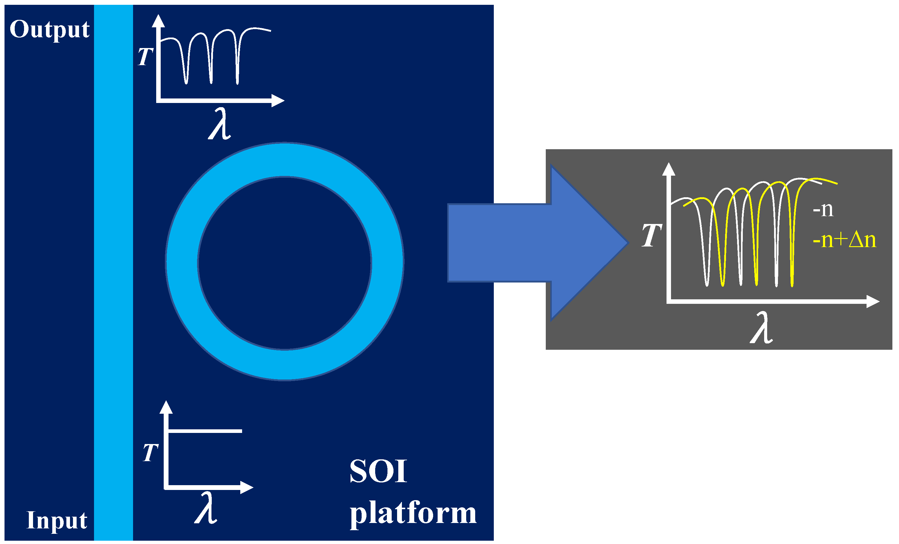
2.1. Optical RR Structures

Biochemical sensing using RRs is a highly interesting technology platform these days. Indeed, the ability to use optical principles and effects comparable to those used in standard straight WGs allows for ultra-high sensor response as well as inexpensive, CMOS-compatible readout approaches. Furthermore, because of the optical field increase in tiny regions, the high Q-factor, and the compact dimensions that characterize overall sensor designs, it is feasible to improve sensing performance. The operational concept in chemical and biochemical sensing is that the presence of a chemical substance being detected close to the sensor surface causes the effective index of the optical mode traveling through the structure to change.
Generally, a Si-based bus WG is side-coupled to a ring structure in a typical RR configuration as shown in Figure 2 (left). A tunable laser or a superluminescent diode’s light is often linked to the bus WG using a grating coupler or butt coupling. If the λres criteria are met, the light is partially linked to the RR, resulting in a λdip in the output spectrum. Depending on the light source, the light is linked to a photodetector or an optical spectrum analyzer at the output. Laser and photodiodes, as well as photonic sensors, may now be implemented on the same chip due to recent improvements in heterogeneous and monolithic assembly [40]. Evanescent field sensing is the general sensing process that underpins their operation. The λres state of the RR is modified if the evanescent field is changed due to the immobilization of analytes on the Si WG, resulting in a λres displacement as shown in Figure 2 (right).
Several computational studies were conducted in the previous decade to enhance WG designs for optical sensing [23]. As shown in Figure 3, three major types of WGs are often utilized. These include strip WGs, rib WGs, and slot WGs. The guided mode’s evanescent field is partially penetrating the upper cladding (UC) material, where the analyte is found. Each WG structure has a variable quantity of light entering the UC, which corresponds with undesirable optical losses, i.e., the more the light enters the UC, the higher the optical losses owing to absorption and scattering. In strip or rib WG structures, for instance, light is mostly limited to inside the high index Si core; however, in slot WG architecture, light can be greatly trapped in the subwavelength low index medium between two Si rails. Compared to ridge WGs, slot WGs have more spatial overlap between the evanescent and perceiving environments, resulting in better S. As a result, slot WGs are a popular choice for bulk index sensing. It is vital to select a suitable WG type established on the need. Low optical losses are achieved at the expense of S in rib WGs. Slot WGs, on the other hand, have a high S but a significant optical loss [13]. Ridge WGs, on the other hand, provide an excellent balance of loss and S, as shown in Figure 3. Generally, the stronger the light–matter interaction, the higher the WG S, but the optical losses also rise.
The polarization state of the light, which is generally either TE or TM, is another critical feature. In SOI-based PIC, the guided light is usually TE-polarized because it has lower optical losses. TM-polarized light, on the other hand, has a higher field overlap with the UC material, where the analytes are placed, which can contribute to enhanced S. It is essential to identify between S of WG and S of RR while trying to enhance the sensing apparatus S. The interaction of the directed light with the surrounding fluid is designated by the former. It considers that if the UC refractive index changes, the effective refractive index of the propagating mode changes as well. The S of WG is calculated as
S WG = Δ n e f f Δ n U C ,
where ∆neff and ∆nUC are the change in the effective refractive index and the change in the refractive index of the UC, respectively. WG enhancement through simulation studies can benefit from such a formulation. Nevertheless, S of RR is not only determined by WG geometry but a supplementary formula for S of RR is also provided by
S R R = Δ λ Δ n e f f ,
When we combine both the formulas, the total S of photonic device is obtained, which is described by
S = S WG S R R = Δ n e f f Δ n U C × Δ λ Δ n e f f = Δ λ Δ n U C ,
It is well-noted that the unit of S is frequently expressed as nm/RIU, where RIU stands for refractive index unit. These descriptions, on the other hand, are specific to the photonic device and not to a measured quantity. The limit of detection (LOD) in this case is determined by the lowest detectable change in the UC refractive index, which is dependent on the minimum measured resonance wavelength change that can be identified by the testing set-up. The sensor performance of slot and strip WG RRs were compared in [30,41]. In [41], glucose levels in blood samples ranging from 10 to 200 mg/dL are numerically monitored using a minimally intrusive approach. The finite element method is also used to predict a six-fold higher sensitivity of the slot WG-based RR. Daoxin Dai presented a unique sensing technique in 2009 by cascading two micro-rings in a manner that functions similarly to a Vernier scale [42].
Multiplexed label-free biosensing was suggested using an array of optical slot-WG RR sensors paired with microfluidic-oriented services in a small device. Physical modeling yielded a volume refractive index LOD of 5 × 10⁻⁶ RIU and a surface mass density DL of 0.9 pg/mm2 due to the slot-WG RRs’ increased S combined with on-chip reference [43]. Subwavelength grating (SWG) WGs were particularly appealing because they allowed the driving mode’s effective index and dispersion properties to be tailored. Due to the improved light–matter interaction, SWG WG-based RRs are extremely sensitive [44,45,46,47]. A 30 μm diameter SWG RR for biomedical application was developed in [46]. It had a device DL of 2 × 10⁻⁶ RIU and a high S of 490 nm/RIU. Integrated photonic sensing devices have been extensively explored in terms of S and reliability over the last twenty years. The placement of the sensing region, which is adjacent to optical and electronic components, is the bottleneck for a transfer from laboratory to industry. This prevents complete packing and renders sensing device handling difficult. A low-cost and scalable packaging technique with a microfluidic network is necessary for the large-scale development of SOI-based RR biosensors [48]. Recent advances in CMOS-compatible epoxy chip-in-carrier techniques [49,50], as well as the fan-out wafer-level (FOWLP) packaging technology, are suitable candidates for this purpose [51]. FOWLP technology is a modification of normal wafer-level packages (WLPs) that was created to give a solution for semiconductor devices that require a higher integration level and a bigger number of external connections. It has a lower package footprint, more input/output (I/O), and better thermal and electrical performance than previous generations. Individual dies are embedded in a low-cost material, such as epoxy mold compound (EMC), with space between each die allotted for extra I/O connection points, avoiding the usage of relatively costly Si real estate to handle a large I/O count. PVD seed deposition and subsequent electroplating or patterning are used to reroute I/O connections on the die to mold compound regions in the periphery, resulting in redistribution layers (RDL). The future study shall concentrate on wafer-level packaging advancements as well as monolithic integration of SOI ring resonators with a laser source, photodetector, and electrical interconnects on the same chip to give a complete lab-on-a-chip platform.
Focusing on an SWG μ-RR, high-S complex refractive index sensing is suggested and experimentally realized, favored with strong Fano λres at 1550 nm wavelength [52]. The μ-RR is made up of trapezoidal Si pillars with a subwavelength period, which improves light-analyte overlap while also providing a high Q-factor. One SWG WG is side-linked with a μ-RR that is supposed to provide a partial Fabry–Perot effect. Figure 4a depicts the ring section, which is made up of trapezoidal Si pillars, and Figure 4b depicts a detailed image of the gap region between the ring and the bus WG. A strong asymmetrical Fano λres is created at a 1550 nm wavelength due to the interplay of the resonant state of the μ-RR and the partial Fabry–Perot effect in the straight WG. High theoretical S of 366 nm/RIU and 9700/RIU for the real portion (n) and imaginary part (k) of the refractive index may be obtained because of the SWG WG structure’s significant light-analyte overlap and the strong asymmetrical Fano λres in the spectrum. The detection of glucose solution concentrations has also been shown experimentally, with a high experimental S of 363 nm/RIU [52]. The devices are submerged in glucose solutions and the spectrum is tested to determine their sensing capability. Deionized water was used to make glucose solutions with concentrations of 2 g/100 mL, 4 g/100 mL, 6 g/100 mL, 8 g/100 mL, and 10 g/100 mL. Figure 4c shows the SWG μ-RR device’s observed transmission spectra in deionized water and glucose solutions [52].
Claes et al. demonstrated this idea by employing large-circumference μ-rings to make it function in a different domain, lowering the LOD [53]. It is developed in an SOI platform with two cascaded RRs, and its S has been proven to be as high as 2169 nm/RIU in an aquatic environment. The application of this principle to an RR sensing device is shown in Figure 4d and the fabricated device is shown in Figure 4e. Two RRs with varying optical roundtrip lengths are cascaded, with the first RR’s drop signal serving as the second’s input. The transmission spectrum of each RR is comb-like, with peaks at the λres. The free spectral range (FSR), or spectral distance between these peaks, is inversely related to the RR’s optical roundtrip; therefore, each resonator in the cascade will have a distinct FSR. This technology has been used multiple times, and very sensitive biosensing devices have been proven to outperform the more typical single-RR sensing devices [54,55,56]. An optical lithography-fabricated slot-WG-based RR in SOI is shown with a footprint of just 13 μm × 10 μm. It has an S of 298 nm/RIU and a LOD of 4.2 × 10⁻⁵ RIU for changes in the refractive index of the upper cladding, according to tests [57]. For the first time, it was illustrated that surface chemistry for selective label-free protein sensing can be adapted within a 100 nm wide slot region, and that using a slot WG rather than a normal WG enhances the S of an SOI RR for protein detection by a factor of 3.5. The RR device, which is shown in Figure 4f, was made using 193 nm optical lithography. When varied salt levels are flown over, Figure 4g illustrates the shift of a λdip in the transmission spectrum of the RR. To find the λres, Lorentzian fitting was applied [57]. Table 1 listed the previously reported RR sensors and their sensing performance.
Figure 4. Recently proposed SOI-based RR sensing devices, (a) images of the manufactured SWG μ-RR device taken using a scanning electron microscope [52], (b) magnified picture of the gap region between the ring and bus WG [52], (c) experimental transmission spectra of the SWG μ-RR device submerged in deionized water and various glucose concentrations (1)–(6) [52], (d) a photonic sensing device made up of two cascaded RRs. Cascaded are two RRs with distinct optical roundtrip lengths. A thick cladding covers the whole chip, leaving only an aperture for one of the two RRs. The sensing device RR will be visible to changes in refractive index in its surroundings, but the filter RR will be insulated from these changes by the cladding [53]. (e) An optical microscope view of the SOI system. Two RRs with a physical roundtrip length of 2.5 mm are cascaded, and the cavity is folded to decrease the footprint. The entire device was coated in 500 nm silicon oxide, then the second RR was carved open [53]. (f) Top-view SEM image of the slot-WG-based RR, (g) for varied salt concentrations, the pass spectrum of the slot-WG-based RR shows a λdip. The Lorentzian fits are presented in black, whereas the observed spectrum is shown in gray [57].
Photonics 09 00331 g004

2.2. Bragg Grating (BG) Structures

The BG is a device that has been known for a long time and has always been recognized as having the capability to be used as a sensing element. These structures are most typically used in optical fibers, reflecting optical wavelengths as per the following relationship:
λB = 2ʌneff,
where λB is the Bragg wavelength at which optimal reflectivity is achieved. The period of the refractive index modulation that defines the grating is provided by ʌ. The effective index of the WG containing the Bragg grating, neff, is a combination of the core and cladding refractive indexes with which the optical mode engages. For a variety of reasons, planar BG devices are suitable for sensing purposes: (1) Multiple wavelengths may be employed, allowing for analyte identification by optical dispersion analyses as well as a range of evanescent field penetration depths, which may provide extra details on biological entity dimensions. (2) On a single sensor chip, many different sensing zones can be included. This is especially helpful in immunoassay-based bio-detection, where it is desirable to test for many targets at the same time without duplicating equipment or incurring time delays. (3) The monolithic Si chip-based technology is rugged, needs no electrical signal, and is chemically resistant, making it appropriate for use in a variety of settings.
The majority of available medical temperature sensing devices’ detecting components are conductors, which are sensitive to EM-interference in certain situations, such as nuclear magnetic field diagnostics. The photon-based sensing device module is made of nonconductive SOI material, which prevents data from being influenced by the electric field environment and has strong research potential in biological and medical research and therapy. μ-scale RRs [61,62], fiber Bragg gratings (FBGs) [63], and WG BGs [64] are among the proposed sensing device technologies. Sensing devices that employ optical signals for diagnosis have the following benefits over standard sensing devices that use electric signals: lightweight, strong anti-EM-interference ability, low power consumption, wide operating frequency range, consistent performance, high speed, low loss, and low crosstalk. A WG BG is easy to embed into a chip and is interoperable with CMOS fabrication techniques [65].
This approach may drastically reduce the WG structure size to a few hundred nm in diameter and increase temperature sensitivity [66]. WG BGs are WG structures that can achieve periodic refractive index variations, hence there are numerous approaches to realizing WG BG in a PIC. It may also be classified into various architectures established on the grating’s period, WG structure, and refractive index distribution. WG surface grating [66] or sidewall grating [67] are commonly utilized grating filters. In comparison, the most employed structure is two-sided WG BG, which corresponds to sidewall grating [68,69]. For a photonic sensing device, three WG BG architectures have been developed [70]. The experiment on the two-sided WG BG was carried out using an experimental platform established on a photonic integrated interrogator. The two-sided WG BG may be used to assess temperature variations across a range of 35–42 °C with a temperature measurement error of 0.1 °C, according to the results. This technique has the potential to make it easier to integrate an SOI WG BG photonic sensing device into wearable technology and enable temperature sensing. Figure 5 depicts the configuration and operation of the PIC of an AWG interrogation.
BGs have been integrated into the SOI platform because of recent advances in Si photonics. Biological or chemical sensing is one of the most promising uses of Si BGs [71]. All of these sensing devices have a distinct absorption spectrum that may be utilized to explore the RI of the cover media. The FP-resonator sensing device, for example, integrates micro or nano channels in the optical cavity immediately built on the Si substrate, making it appropriate for both volume and surface sensing. Established on the strip and slot WG, a downsized design of an FP-resonator is numerically investigated [68]. The grating depth and number of periods have a substantial influence on the sensing device’s spectral properties, according to this study on design parameter dependency. An FP-resonator with 30 grating periods established on slot WG achieves the greatest S of 30 nm/RIU. Increase the depth of the grating up to a specified limit and the number of periods to increase S and figure of merits [68].
In planar form, only a few numbers of BG-based devices have been researched and built. They’ve been established in polymers [72], sol-gel systems [73], SOI [64,74], Lithium Niobate [75], and Silica-on-Silicon [76,77], among other material systems. The waveguiding and grating structures in Bragg-based optical sensors have been manufactured using a variety of methods, including ridge WGs [78], UV written WGs and gratings [77], corrugated or etched BGs [79,80], and even BGs via selective nanoparticle precipitation [81].

2.3. Mach–Zehnder Interferometer (MZI) and Young’s Interferometer (YI) Structures

Because they integrate two very sensitive methods, wave-guiding and interferometry techniques, interferometer-based biological sensing devices are one of the most reactive compact optical systems. In a conventional interferometric biosensor, a Y-junction separates the traveling light into two single-mode WG pathways, one of which includes the sample and is known to be the sensing arm, while another is known as the reference arm. The evanescent field of the sensor arm interfaces with the specimen and identifies a variation in refractive index at the surface, causing an optical phase change. After traveling a given distance, the beams recombine, producing constructive or destructive interference at the output, with the intensity modulation matching the refractive index difference between both the sample and reference arms. Biological materials are usually dissolved in water; this is the most popular cover media for biosensors that have refractive indices that are similar to those of water. Different materials can be employed to absorb the measurand and thus bring about a change in the refractive index of the solid in other types of sensors, such as gas sensors. For instance, surface plasmon resonance may be utilized to detect methane using PDMS doped with cryptophane-A [82,83].
In the early 1990s, Heideman et al. developed the first biosensing application established on integrated MZIs [84]. Since then, the manufacture of MZI sensing devices has progressed significantly. Various structures with an LOD of 10−6 to 10−7 RIU have been successfully designed by employing a variety of fabrication materials, including Si3N4 [85], TiO2 [86], Si [87], and polymers [88]. In contrast, chip-based YIs revealed the ability to detect biomolecules, resulting in a LOD equivalent to the MZI sensing device [89]. In a follow-up investigation in 2000, Brandenburg et al. employed Si oxynitride as WGs to lower the LOD of YI devices to 9 × 10⁻⁸ RIU [90]. With the minimum possible LOD of 9 × 10⁻⁹ RIU, Schmitt et al. reported Ta2O5-based YIs to further enhance sensing capacity [91]. In recent years, polymeric materials have been employed in YI sensing devices, resulting in a low-cost, mass-production-ready technology with adequate S [92]. The integrated sensor’s responsivity and interferometric stability are compared to that of a fiber-based interferometer using an electrochemical etching and laser oxidation approach to build channel WGs and integrated on-chip MZI structures [93]. The detection capability is measured by selectively adding isopropanol to a 200 m long WG section in one arm of the interferometer, which results in a 9.7 π phase shift. In comparison to a comparable fiber-based approach, the integrated interferometer provides a steadier response.
A label-free MZI biosensor established on Si nitride slot WG was proven to be highly responsive [86]. Unlike ordinary MZI sensing devices, the detecting arm of the MZI structure was built from a slot WG, while the reference arm was constructed from a regular ridge WG. Owing to the slot WG’s feature of delivering significant optical intensity in the low refractive index slot area, permitting high light–-matter interaction, higher S might be gained by using it as a sensing zone. The bulk refractive index S of the slot WG MZI sensing device was 1864 π/RIU using a 7 mm long slot WG sensing arm, which is greater than the typical MZI sensing device established on the Si nitride substrate. The biosensing capabilities of the newly created slot WG MZI were investigated using biotin–streptavidin binding. The S of the method was demonstrated to be as low as 18.9 fM or 1 pg/mL of streptavidin solution. A new design for an on-chip optical temperature sensing device established on a Mach–Zehnder interferometer is described in [94], with the two arms consisting of hybrid WGs that provide opposing temperature-dependent phase shifts to improve the sensor’s temperature S. The manufactured sensing device with Si–polymer hybrid WGs has a S of 172 pm/°C, which is twice as high as a traditional all-Si optical temperature sensing device (80 pm/°C). Furthermore, a system using Si–titanium dioxide hybrid WGs is projected to have a S of up to 775 pm/°C, according to calculations. The suggested design is found to be both design-flexible and manufacturing error-resistant. The SEM image of the proposed sensing device design is shown in Figure 6a [94].
Based on long-range surface plasmon polariton (LRSPP) WGs, two integrated YI sensing devices are proposed in [95]. The first sensing device is single-channel and uses a Y-junction splitter, whereas the second has a corporate feed structure and is multichannel. The multichannel YI allows for phase-based monitoring of refractive index variations in numerous channels simultaneously and in different ways. The WGs’ diverging output beams are overlapping in the far-field to generate interference patterns, which are then postprocessed to extract phase values using the fast Fourier transform technique. The sensing capabilities of these YIs were established by injecting fluids with a varying refractive index into the sensing channels in a systematic fashion. For both LRSPP-based YIs, an LOD of 1 × 10⁻⁶ RIU was achieved, which is a significant increase above measurements from identical structures utilizing attenuation-based sensing [95]. Figure 6b,c depicts the corporate-feed multichannel structure, which includes four sensing channels represented by etches on WGs and two reference channels represented by cladded WGs. Two Y-junction splitters are cascaded to a first Y-junction structure to create the corporate feed structure [95]. Figure 6d–g shows how to create interference patterns for the corporate-feed YI by gradually changing the distance L between the convex lens and the camera. When no convex lens is installed after the microscope objective, the outputs from the corporate-feed multichannel WG are initially collimated, generating six beams, each with varying power, as illustrated in Figure 6d. After that, a convex lens is placed. For L < f, the beams approach each other, where f is the focal length of the convex lens (Figure 6e) [95]. For L = f, they overlap at the focal point (Figure 6f) [95]. The beams diverge and create an interference pattern on the camera when L > f (Figure 6g) [95]. Previously proposed MZI and YI sensors and their sensing performance are reported in Table 2.

2.4. Photonic Crystals (PhCs) Sensing Devices

Photonic sensing devices have grown in popularity in recent times of an increased demand for sensing applications in defense, healthcare, food quality monitoring, and aerospace, to mention a few [2,33,103,104,105,106,107]. The detailed introduction on PhC photonic devices can be found in [108]. PhC is a periodic-modulated dielectric nanostructure material that may be manipulated to form PBG, which prevents light from traveling at specified wavelengths. As a result, a diverse variety of PhC-based devices, including filters [109,110], electro-optical modulators [111], switches [112,113], and delay devices [114], have been widely employed in light flow control applications [22]. PhC-based sensing devices appear to be growing exponentially due to their appealing features such as ultra-compact size, high measurement S, structural design freedom, and suitability for monolithic integration [115]. Furthermore, PhC-based devices can inherit the advantages of optical sensing devices, such as safety in flammable explosive environments, immunity to electromagnetic interference, long-range tracking, and quick reaction time.
Consequently, the PhC surface’s local optical modes may be employed in life science research as a very sensitive, label-free platform for biosensing and bioimaging. High-performance sensing devices can be built using PhCs [2]. A variety of photonic sensing device topologies have been thoroughly investigated and used in biosensing. PhCs have a tiny footprint yet provide strong optical confinement, allowing chemical analytes to be recognized. Furthermore, cutting-edge chemical surface functionalization technologies and integration with microfluidic systems may be used to achieve amazing performance in tiny sensing device chips. A PhC μ-cavity sensing device with a total size of 50 μm2 and an effective detection area of 0.272 μm2 was used to perform a time-resolved label-free analysis of protein binding in a physiological buffer [116]. This ultracompact sensing device is used to assess an affinity constant of 6.94 × 10⁷ M−1 for anti-biotin binding to biotinylated-bovine serum albumin (b-BSA). Researchers all around the globe are investigating refractive index biosensors on PhC, and numerous sophisticated sensing device designs, such as integrated μ-cavities [116] and interferometers [117], have been anticipated for refractive index sensing applications. These devices provide several advantages, including little specimen preparation and no fluorescent labeling, as well as excellent S. The sensing technique is established on the detection of refractive index fluctuations in a bulk solution caused by chemical analytes.
Because of its large surface area and variable surface chemistry, porous Si can be employed as a biosensor. Porous Si is a Si wafer with nanopores embedded in its μ-structure. Electrochemical etching of Si wafers in HF electrolyte under an applied electric current is a simple way to make it. By modifying the etching current density, time interval, and HF concentration, the electrochemical technique enables fine control over porous Si parameters such as porosity and thickness of the porous layer. By altering the current density periodically during the electrochemical process, a 1D-PhC established on multilayered porous Si may be readily constructed [118]. The porous Si 1D-PhC has several benefits, including a large specific surface area, simplicity of manufacture, and compliance with common microelectronics technology [118,119,120]. R. Caroselli et al. established a very sensitive PhC sensing device for modest refractive index fluctuations established on porous Si. The S of the porous Si sensing device was around 1000 nm/RIU [121].
V. Pham et al. also created a porous Si multilayer-based 1D-PhC μ-cavity sensor. The S of the 1D-PhC sensing device was around 200 nm/RIU, and it may be utilized to determine the organic content of various liquid solutions [122]. Furthermore, Tamm λres, a well-known phenomenon, has been realized in PhCs and is being exploited in optical sensing approaches for PhC architectures [123,124,125]. Tamm λres is mostly created at the metal-Bragg mirror interaction. B. Auguie et al. investigated Tamm λres in a PhC made up of SiO2 and TiO2 multilayers both theoretically and practically. This structure’s S was poor, at around 55 mm/RIU [126]. Based on Tamm/Fano λres, a new metal porous Si-1D-PhC liquid sensing device has been developed. In the mid-infrared spectral region, the operational wavelength range is 6.35 μm to 9.85 μm [127]. To display Tamm/Fano λres more clearly, several metals (Al, Ag, Au, and Pt) are added to the top surface of the porous Si-1D-PhCs structure. It is the first time that Tamm/Fano λres appear simultaneously in porous Si-1D-PhCs inside the same structure. The transfer matrix method (TMM) and Bruggeman’s effective medium assumption were used to determine the reflection spectra for the metal porous Si-1D-PhC structure. The Tamm/Fano λres perform a redshift towards higher wavelengths as the refractive index of the pores increases, according to the numerical simulations. The Ag porous Si-1D-PhC sensing device delivered the best results. With a high Q-factor of about 2149.27, its S may be increased to 5018 nm/RIU [127]. Table 3 summarizes the previously developed PhC refractive index sensing devices and their sensing performance.
The periodic air hole microstructure of the PhC cavity is a suitable choice for housing gas analytes; hence, the resonant wavelength of the PhC cavity, including the refractive index of the air hole, would oscillate with infiltrating gas concentration or ambient pressure fluctuation. This is also the measuring concept of a PhC cavity-based gas sensing device, and the footprint of this sensing device might be considerably decreased when compared to a typical optical gas sensing device [136]. On the SOI substrate, the design, manufacturing, and characterization of a multi-slot PhC cavity sensing device are given in [137]. By adjusting the geometry of the PhC cavity, most of the light may be concentrated in the lower index area, significantly improving S. It was discovered that the wavelength shift per RIU for the sensing device is 586 nm/RIU, achieved by introducing the cavities to varying mass concentrations of NaCl solutions, which is one of the greatest sensitivities reported in a non-suspended cavity. Additionally, the disclosed sensing device’s detecting region is only 22.8 μm 1.5 μm in size, making the high-S PhC cavity sensing device appealing for the fabrication of on-chip sensing device arrays. The device layout was developed using direct-writing 100 keV E-beam lithography (JEOL JBX-6300FS) with a positive tone ZEP-520A resist and replicated onto the underlying Si layer by an anisotropic inductively coupled plasma method using an SF6/C4F8 gas combination. As shown in Figure 7a, properly constructed grating couplers for TE polarization are fabricated to evaluate the efficacy of the multi-slot PhC cavity [137]. For normalization, strip WGs with TE-type grating couplers were also built on the same chip. SEM images of the cavity and an expanded view of the coupling region linking the strip or slot WGs are shown in Figure 7b and Figure 7c, respectively [137]. The completely etched TE-type focusing subwavelength grating coupler is shown in Figure 7d [137].
Development of high MIR PhC-based slotted-WG coupled-cavity sensor acting as a refractive index sensing device is presented in [138], as shown in Figure 7e. The S of the sensor is determined by sensing the change in the λres as a function of refractive index alterations in the region around the cavity. In comparison, MIR PhC-based slotted-WG coupled-cavity exhibits better S to refractive index changes than MIR PhC-based slotted-WG. The S can be increased from 938 nm/RIU to 1161 nm/RIU within the range of n = 1–1.05, with an expansion of 0.01 RIU in the wavelength range of 3.3651 μm to 4.1198 μm, by establishing a μ-cavity within the proposed structure, a calculated Q-factor of 1.0821 × 10⁷ that gives a sensor FOM of up to 2.917 × 10⁶. Additionally, the overall S of 1343.2 nm/RIU is computed for higher refractive indices of analytes within the range of n = 1–1.2 with a 0.05 RIU step [138].
A unique capsule-shaped sensor used for detecting the levels of glucose in the human body is demonstrated in [139]. The model under consideration was developed depending on the index change in the refractive index caused by a change in the material that entered the cavity. The alteration in the index of refraction is followed by a variation in resonant wavelength. The proposed model considers the basic structure and ease of fabrication, as well as other factors, such as S and a low detection limit, as shown in Figure 7f [139]. The results show a high S of 546.72 nm/RIU, a high Q-factor of 2066.24, a low LOD of 1.44 × 10⁻⁴ RIU, and a high transmission value of 97 percent, all of which are usually required and efficient in detecting measured material. This suggested approach offers great potential and appears to be viable to produce various sorts of sensing detecting devices.
A PhC nanocavity with a high Q-factor of 100,000 and a modal volume of 0.71 cubic wavelengths was demonstrated in [140]. A point-defect cavity in a 2D-PhC slab has been further enhanced using a cavity design rule that was recently found, where the configuration of six air holes along the cavity margins is fine-tuned. The predicted modal volume remains nearly unchanged, while the measured Q-factor for the intended cavity is multiplied by a factor of 20 when compared to a cavity without displaced air holes. Figure 7g (left) shows SEM images of one of the manufactured samples, which demonstrate the point-defect cavity with a displacement of air holes A, B, and C. As illustrated in Figure 7g (right), a line-defect WG was also introduced near the point-defect cavity [140].
Despite the growing popularity and considerable promise of PhC cavity-based optical sensing devices, numerous important issues for their practical use remain, including manufacturing defects, coupling issues, and temperature effects. PhC-cavity-based sensors, for example, may be probed in two ways. The wavelength interrogation mode is the first, and the intensity interrogation mode is the second. The optical readout in the first approach involves utilizing an optical spectrum analyzer (OSA) to examine the wavelength of the optical signal whereas, in the second approach, a photodetector (PD) is used to monitor the intensity variations of the output signal. The durability of PhC cavity resonant characteristics against manufacturing faults is a crucial element in real deployments. With today’s PhC manufacturing technology, the position and size of the air hole may be regulated to 1 nm [141] and 2–4 nm [142], respectively. D. Pergande et al. revealed that changes in the radii of the holes reduced the total transmission of bulk PhC [143]. Furthermore, a 1% change in pore radius results in a 15 dB/mm attenuation in transmission. Because the interaction intensity between the optical field and the material of the defective area is rather strong, fabrication defects in the cavity region of the PhC cavity will have a significantly greater influence on the resonant capabilities of the PhC cavity. For instance, Hagina et al. proved that introducing a 1 nm defect in the hole radii reduced the eventual Q-factor of a heterostructure PhC cavity to one-eighth of the ideal one [144]. Furthermore, PhC WG manufacturing defects are intricate, random, unexpected, and immeasurable, thus, ways to ease manufacturing and attain feasible tolerances are essential future topics.
Before the actual implementation of the PhC cavity, one additional problem is the efficient coupling of light from traditional single-mode fiber (SMF) into the PhC cavity device [145]. One of the most frequent ways to reduce coupling loss is to insert PhC WGs on both sides of the PhC cavity. The light is first emitted from a typical SMF to a PhC WG, and then transferred from the PhC WG to the PhC cavity. Nevertheless, it poses problems since the usual WG cross-section (1 μm width and 500 nm thickness) makes light coupling in and out of the SMF core (8–10 μm diameter) impossible. Significant challenges arise because of the differences in transmission principles between PhC WG (based on PBG theory) and SMF (based on total internal reflection). Generally, coupling loss may be considerably reduced by accurately aligning SMF with the PhC device using an adaptable mechanical device and constructing the coupling interface properly.
Because Si’s refractive index is thermally dependent, the resonant qualities of Si-based PhC cavity devices are altered by surrounding temperature [146]. To prevent unwanted fluctuation, a precise temperature control system is required in real applications, which will increase the size and expense of the PhC cavity-based sensors. This impact was not considered in prior studies until 2009 when C. Karnutsch et al. suggested a temperature-insensitive PhC cavity based on optofluidic technology [147]. It was proved that the thermo-optic effect of the infiltrating optofluidic might diminish or even remove the temperature dependency of the device for a specified operating range, by engineering adequate dimensions and utilizing a liquid with an adequate thermo-optic coefficient. However, the use of an optofluidic-infiltrated PhC cavity may limit the flexibility of the PhC cavity in structural design. As a result, reducing the temperature’s impact will be a major issue in the future. With the advancement of PhC manufacturing technology, considerably better design plans for PhC cavities will be offered, and many more PhC-based optical sensors will be suggested. The key developments of PhC-based optical sensors in the future will be controllability, network, integration, all-fiber, real-time evaluations in fluidic environments, and research into novel mechanisms and methodologies.

3. Si-Based MIR Gas Sensing Applications

The MIR wavelength region is a hot issue in frontier research right now. Its use spans a wide range of mid-IR industrial and biomedical sensing applications. Most complex molecules, such as those present in food, tissue, or catalytic substances, have vibrational spectra in the mid-IR, making them detectable via mid-IR spectroscopy. In addition, the basic absorption bands of gas molecules are situated in the mid-IR, allowing for the use of unique instruments for mid-IR gas spectroscopy at low concentrations, which is useful in areas such as in “leak-tests” or greenhouse gas remote sensing. The absence of effective mid-IR excitation light sources and sensitive mid-IR detectors and imaging has been the major impediment to utilizing the mid-IR optical window in the past.
Due to its simple inclusion with Si electronics, high index contrast, small footprint, and low cost, as well as its optical transparency in the near-infrared and parts of the MIR wavelengths (from 1.1 to 8 μm), Si has been the best material for the photonics industry over the last decade. While device parameter variations caused by micro- and nanofabrication, as well as a higher than desired propagation loss, remain a barrier in many on-chip data transmission applications, sensors do not expect the same amount of scrutiny. Because of these benefits, Si PICs have seen their practical implications expanded in recent years to include gas sensing, biosensing, and biomedical diagnostics. Due to a scarcity of elements in other wavelengths, which restricts the efficiency of these photonic systems, the Si photonic devices employed in telecommunication wavelengths are often preserved for most of these new applications. A Si photonic on-chip sensor for EFA spectroscopy of CH4 around 1.65 μm, for example, has recently been developed [148]. A 10 cm long Si spiral WG is used to achieve a S of 756 ppmv.Hz−1/2. Because the absorption coefficient of CH4 at these longer wavelengths is substantially greater than at 1.65 μm, extending the operation wavelength of the Si photonic on-chip sensor to roughly 2.35 μm or 3.25 μm will permit a more compact on-chip sensor with better S [14].
Photonic devices on chips are progressively being established for chemical and biological sensing, with performance metrics that approach benchtop equipment, implying the possibility of transportable, hand-held, and wearable monitoring of a variety of chemical and biological samples [149]. For several application areas in civilian and military domains, trace gas detection based on molecular absorption spectroscopy is of tremendous interest. Due to the existence of fundamental vibration traces of practically all chemical bonds in this wavelength range, the MIR spectrum is sometimes referred to as a “molecular fingerprints” zone [13,150]. Most optical gas sensors rely on absorption spectroscopy, which detects a gas by evaluating the light absorbed as a function of wavelength (owing to its interactions with the gas) [151]. The absorption lines of many major organic and inorganic compounds in the MIR spectral range (2–20 m) (Figure 8) relate to basic vibrational and rotational energy transitions. The line strengths of MIR fundamental transitions are higher than those of their overtones, which are generally employed in the visible and near-IR areas [152,153]. Furthermore, spectra are less cluttered, permitting the selective identification of multiple compounds via spectroscopy [152,153]. MIR gas sensors are becoming increasingly popular for a variety of chemical analysis applications, including industrial process control [151,154,155], environmental monitoring [156,157], and medical diagnostics [158], due to their molecular “fingerprinting” capacity.
Long-wave infrared (6–14 μm) has great benefits for biochemical sensing since it covers a wide range of molecule absorption signatures [159]. WGs are an appealing chip-scale downsizing approach for optical sensors. Nevertheless, research on WG devices in this wavelength range is restricted. A suspended Si WG anchored by subwavelength grating (SWG) metamaterial claddings is used to construct a long-wave infrared photonic platform for quick and sensitive on-chip gas detection, as shown in Figure 9a–c [9]. This technology offers a practical method for fully using Si’s transparency window. The SWG structure offers a viable method for engineering the mode profile for strong light–analyte interaction. In the broad spectral region of 6.4 μm–6.8 μm, propagation loss and bending loss are explored. Grating couplers, for example, are useful devices. Y-junctions and directional couplers are also shown [9]. For instance, toluene vapor detection is used to demonstrate sensing that utilizes the technology. The detection limit corresponds to 75 ppm. Toluene at 75 ppm takes approximately 0.8 and 3.4 s to respond and recover, respectively [9]. The impressive results demonstrate that the system is a good fit for on-site medical and environmental applications.
On the MIR silicon-on-sapphire (SOS) framework, RRs have been realized [160,161,162]. Spott et al. published the first MIR SOS RR in 2010 [161]. The ring has a radius of 40 μm and a 0.25 μm edge-to-edge spacing. For λ = 5.4 to 5.6 μm, the experimental results revealed Q-factor = 3000, FSR at about 29.7 nm, and an associated group index of 3.99 [161]. A computational analysis of the design of a suspended membrane waveguide (SMW) made of SOI was performed in [159]. Using a 3D finite element approach, the WG architecture is tailored at 3.39 μm TE-polarized light, which is the absorption line of CH4 gas. The WG’s transmission loss (TL) and evanescent field ratio (EFR) are determined by various geometric factors such as core width, height, and cladding period. The relationship between TL and EFR has been discovered. As a result, WG architecture may be engineered to provide high EFR at the expense of high TL, or low EFR at the expense of low TL, as required [159].
For the monitoring of trace gases, optical WGs founded on the SOI platform provide an attractive substitute that uses EFA sensing. Gas sensors based on EFA can only operate if the gas in question has a specific absorption line at the operating wavelength. Furthermore, the optical attenuation at a certain wavelength is proportional to the gas concentration. The Beer–Lambert law, which is generally dependent on the gas concentration, length, and evanescent field ratio (EFR) of the WG, may be used to represent the power decay [163]. As a result, EFR is an important metric for detecting gas sensors based on EFA. The EFR is the ratio of the targeted region’s intensity integration to the WG structure’s overall intensity integration and can be written as:
E F R = d e s i r e d | E ( x , y , z ) | 2 d x d y d z t o t a l | E ( x , y , z ) | 2 d x d y d z
Several gas sensors based on optical WGs [12,164,165,166,167] and optical fiber have been suggested to study this phenomenon. To manufacture gas sensors, there are multiple WG systems based on various platforms that may be used. Based on the concept of total internal reflection, the dielectric WG can direct light in a high refractive index core. At high WG cross-sections, these WGs enable significant mode confinement and typically minimal propagation loss. The evanescent field overlap in the ambient medium should be strong for highly sensitive EFA gas sensors. The propagating mode’s evanescent field can be increased by lowering the WG geometry at the expense of significant propagation loss. Furthermore, diffraction limits the capacity of these WGs to contain light.
Low evanescent field and high propagation loss may be solved with a hybrid plasmonic WG (HPWG) construction. A thin film of low index material (for instance SiO2) is layered between high refractive index material (such as Si) and metal in this WG (typically silver or gold). The horizontal and vertical variants of the HPWG are both possible. Air (n = 1.0) can be utilized as a low index material between metal and high index material in the horizontal layout. These WGs are extremely appealing for gas sensing applications because a hybrid mode is restricted in a low index nano-slot that may directly interact with the ambient medium. We established an EFR of 0.55 in prior work on strip, rib, and slot WGs [12,13,14,164]. For the monitoring of lethal CH4 gas, the EFR is improved in a more responsive dual-HPWG structure [165]. The WG shape is tuned for the absorption line of CH4 gas, which is λ = 3.392 μm. The modal parameters of a conventional ridge WG, such as EFR, E-field distribution, confinement factor, and propagation loss, are estimated. By placing gold rail on both sides of the core parted by a nano-gap, the ridge WG is changed into a dual-HPWG. With a propagation loss of 0.7 dB/μm, an enhanced EFR of 0.74 is achieved. Determining the degradation in transmission power due to absorption by the gas in the medium yields a S of 0.0715 (mW/concentration) for the proposed WG design [165].
For hydrocarbon emission control, a chip-scale MIR sensor was created in [168]. Amorphous Si optical strip WGs were used in the sensor, which was made using CMOS methods. Through λ = 2.70 μm to 3.50 μm, the WG showed a strong fundamental mode. CH4 and acetylene measurements were used to assess its sensing capabilities. The distinctive C–H absorption bands associated with CH4 and acetylene were discovered at λ = 3.29 μm–3.33 μm and λ = 3.00 μm–3.06 μm, respectively, established on spectral mode attenuation. At λ= 3.02 μm and 3.32 μm, real-time CH4 and acetylene concentration monitoring were also accomplished. As a result, the MIR WG sensor allowed for precise and fast hydrocarbon gas combination analysis. The width and height of the WG was 10 μm and 1 μm, respectively, with a well-cleaved end facet, which was crucial to limit the optical loss produced by scattering, as seen in the cross-sectional SEM picture in Figure 9d [168]. The butt-coupling efficiency between the 9 μm core diameter MIR fiber and the WG was enhanced by the 10 μm WG width. The asymmetric C–H stretching generated by C2H2 resulted in a significant absorption coefficient from λ = 3 μm to 3.08 μm. Due to the asymmetrical C–H vibration, the mode intensity for CH4 fell between λ = 3.18 μm and 3.40 μm. The significant R branch and the mild P branch of CH4 were ascribed to the absorptions detected at λ = 3.32 μm–3.40 μm and 3.18 μm–3.30 μm, respectively (Figure 9e) [168].
A polarization-independent HPWG tailored for λ = 3.392 μm, which corresponds to the CH4 gas absorption line is designed in [169] as shown in Figure 9f. Both TE and TM-hybrid modes can benefit from the WG design’s high mode S and EFR. The WG’s modal analysis is carried out using finite element methods in 2D and 3D models. The TE-hybrid mode can achieve mode S and EFR of 0.94 and 0.704, respectively, with adjusted WG variables, whilst the TM-hybrid mode can achieve mode S and EFR of 0.86 and 0.67, respectively. At 60 percent gas concentration, a 20-μm-long HPWG can dissipate 3 dB of power in the TE and TM hybrid modes as shown in Figure 9g and Figure 9h, respectively. The very sensitive WG system suggested in this work is thought to circumvent the polarization-controlled light’s limitations and might be used in gas sensing applications [169]. At 2.75 μm wavelength, μ-RRs on SOS were described [162]. The SEM image of the manufactured RR structure and ridge WG is shown in Figure 9i and Figure 9j, respectively. The resulting E-field mode profile, as illustrated in Figure 9k, was estimated using the finite element method. A Q-factor of 11,400 ± 800 was achieved. SOS wafer epitaxial Si thermo-optic coefficient was measured to be 2:11 ± 0.08 × 10⁴ K−1. Using a fixed wavelength source, a characterization approach for measuring the Q-factor of μ-RRs is also given. A MIR RR’s Q-factor may be measured simply by changing the device’s temperature. In situations when tunable lasers are not readily accessible, the suggested approach provides an alternate way of Q-factor measurement for μ-RRs in the MIR. At 2.75 μm wavelength, the approach was utilized to evaluate the Q-factor of SOS μ-RR [162].
Figure 9. Si-MIR sensing devices, (a) suspended Si-WG gas sensing platform, which includes grating couplers, tapers, a power splitter (Y-junction), and spiral WGs, is depicted schematically. Inset: a cross-sectional view of the WG taken using an SEM [9], (b) optical picture of the Si spiral WG floating in mid-air [9], (c) a zoomed-in image of the sensing WG encircled by toluene molecules, as shown in Figure 8a by the yellow square box [9], (d) SEM photo of the Si WG [168], (e) when N2, C2H2, and CH4 were used, the WG mode intensities were measured. C2H2 showed strong intensity attenuation between λ = 3 μm and 3.08 μm, while CH4 showed strong intensity attenuation between λ = 3.29 μm and 3.33 μm [168], (f) HPWG enclosed in a gas sensor cell [169], (g) TE hybrid mode power variation vs. gas concentration [169], (h) TM hybrid mode power variation vs. gas concentration [169], (i) SEM picture of a racetrack RR [162], (j) WG cross-section as seen using an SEM [162], (k) FEM-calculated E-field mode profile of the matching quasi-TE mode [162].
Photonics 09 00331 g009

4. Conclusions

This review presents the recent developments of silicon (Si) photonics sensing devices working in near-infrared (NIR) and mid-infrared (MIR) ranges. The functional characteristics of optical Si sensors, which are frequently realized and established on channel WGs in the silicon-on-insulator (SOI) structure, have advanced significantly in recent years. Compact size and convergence of excellent technological characteristics, as well as the ability of mass manufacturing to employ CMOS microelectronics and nanophotonics, are among its advantages. Typically, the working mechanism of the optical WG-based sensing devices is established on the effective refractive index of the propagating optical mode, which is dependent on the concentration of the measured substance or an external physical parameter, including temperature. Slight changes in the refractive index can be perceived by utilizing WG optical sensors established on microelectronics, nanophotonics, and integrated optics technologies. In the first part of the paper, several vital optical elements such as ring resonators, Bragg grating, Mach–Zehnder interferometer, Young’s interferometer, and photonic crystals established on Si platforms working in the NIR range were discussed for biosensing applications. These devices are imperative due to their enhanced device performance and compact size. In the second part of the paper, Si WG-based devices working in the MIR range were discussed for gas sensing applications. Among others, slot WG, hybrid plasmonic WG and suspended membrane waveguide (SMW) are highly sensitive structures to be employed in gas sensing due to their enhanced light–matter interaction. Several novel Si-based gas sensing devices were presented, which are established on these WG structures that offer high S and Q-factor. We believe that this review will be beneficial for the researchers working on Si WG-based sensing devices for both bio- and gas-sensing applications.

Author Contributions

Conceptualization, S.N.K., M.A.B. and N.L.K.; methodology, M.A.B., S.N.K. and N.L.K.; software, M.A.B., S.N.K. and N.L.K.; validation, M.A.B., S.N.K. and N.L.K.; formal analysis, M.A.B. and N.L.K.; investigation, M.A.B., S.N.K. and N.L.K.; resources, M.A.B., S.N.K. and N.L.K.; data curation, M.A.B. and N.L.K.; writing—original draft preparation, M.A.B. and N.L.K.; writing—review and editing, M.A.B. and S.N.K.; visualization, M.A.B., S.N.K. and N.L.K.; supervision, M.A.B. and N.L.K.; project administration, M.A.B., S.N.K. and N.L.K.; funding acquisition, M.A.B. and S.N.K. All authors have read and agreed to the published version of the manuscript.

Funding

This work was financially supported by the Ministry of Science and Higher Education of the Russian Federation under the Samara National Research University (project FSSS-2021-0016) in the overview and comparative parts and under the FSRC “Crystallography and Photonics” of the Russian Academy of Sciences (the state task No. 007-GZ/Ch3363/26) in the part of sensing devices.

Institutional Review Board Statement

Not applicable.

Informed Consent Statement

Not applicable.

Data Availability Statement

Not applicable.

Acknowledgments

We acknowledge the equal contribution of all the authors.

Conflicts of Interest

The authors declare no conflict of interest.

Abbreviations

SOI = Silicon-on-insulator; Si = silicon; PIC = photonic integrated circuit; CMOS = complementary metal oxide semiconductor; WG = waveguide; EFR = evanescent field ratio; EFA = evanescent field absorption; TL = transmission loss; S = sensitivity; LOD = limit of detection; FOM = figure of merit; Q-factor = quality factor; FWHM = full width at half maximum; SiO2 = silicon dioxide; HPWG = hybrid plasmonic waveguide; PhC = photonic crystal; BG = Bragg grating; RR = ring resonator; MZI = Mach–Zehnder interferometer; YI = Young’s interferometer; MIR = mid-infrared; NIR = near-infrared; PBG = photonic bandgap; SMW = suspended membrane waveguide; TE = transverse electric; TM = transverse magnetic.

References

  1. Butt, M.A.; Khonina, S.; Kazanskiy, N. Optical elements based on silicon photonics. Comput. Opt. 2019, 43, 1079–1083. [Google Scholar] [CrossRef]
  2. Butt, M.A.; Kazanskiy, N.L. Two-dimensional photonic crystal heterostructure for light steering and TM-polarization maintaining applications. Laser Phys. 2021, 31, 036201. [Google Scholar] [CrossRef]
  3. Dai, D.X.; Wang, S.P. Asymmetric directional couplers based on silicon nanophotonic waveguides and applications. Front. Optoelectron. 2016, 9, 450–465. [Google Scholar] [CrossRef]
  4. Dan, L.; Citrin, D.S.; Hu, S. Compact high-performance polarization beam splitter based on a silicon photonic crystal heterojunction. Opt. Mater. 2020, 109, 110256. [Google Scholar]
  5. Chen, G.R.; Choi, J.W.; Sahin, E.; Ng, D.T.; Tan, D.H. On-chip 1 by 8 coarse wavelength division multiplexer and multi-wavelength source on ultra-silicon-rich nitride. Opt. Express 2019, 27, 23549–23557. [Google Scholar] [CrossRef]
  6. Butt, M.A.; Khonina, S.N.; Kazanskiy, N.L. Compact design of a polarization beam splitter based on silicon-on-insulator platform. Laser Phys. 2018, 28, 116202. [Google Scholar] [CrossRef]
  7. Chiang, L.-Y.; Wang, C.-T.; Lin, T.-S.; Pappert, S.; Yu, P. Highly sensitive silicon photonic temperature sensor based on liquid crystal filled slot waveguide directional coupler. Opt. Express 2020, 28, 29345–29356. [Google Scholar] [CrossRef]
  8. Janeiro, R.; Flores, R.; Viegas, J. Silicon photonics waveguide array sensor for selective detection of VOCs at room temperature. Sci. Rep. 2019, 9, 17099. [Google Scholar] [CrossRef]
  9. Liu, W.; Ma, Y.; Chang, Y.; Dong, B.; Wei, J.; Ren, Z.; Lee, C. Suspended silicon waveguide platform with subwavelength grating metamaterial cladding for long-wave infrared sensing applications. Nanophotonics 2021, 10, 1861–1870. [Google Scholar] [CrossRef]
  10. Westerveld, W.J.; Hassan, M.M.U.; Shnaiderman, R.; Ntziachristos, V.; Rottenberg, X.; Severi, S.; Rochus, V. Sensitive, small, broadband and scalable optomechanical ultrasound sensor in silicon photonics. Nat. Photonics 2021, 15, 341–345. [Google Scholar] [CrossRef]
  11. Butt, M.A.; Khonina, S.N.; Kazanskiy, N.L. Sensitivity enhancement of silicon strip waveguide ring resonator by incorporating a thin metal film. IEEE Sens. J. 2020, 3, 1355–1362. [Google Scholar] [CrossRef]
  12. Butt, M.A.; Khonina, S.N.; Kazanskiy, N.L. Ultrashort inverted tapered silicon ridge-to-slot waveguide coupler at 1.55 micrometer and 3.392 micrometer wavelength. Appl. Opt. 2020, 59, 7821–7828. [Google Scholar] [CrossRef] [PubMed]
  13. Butt, M.A.; Khonina, S.N.; Kazanskiy, N.L. Silicon on silicon dioxide slot waveguide evanescent field gas absorption sensor. J. Mod. Opt. 2018, 65, 174–178. [Google Scholar] [CrossRef]
  14. Butt, M.A.; Khonina, S.N.; Kazanskiy, N.L. Modelling of rib channel waveguides based on silicon-on-sapphire at 4.67 um wavelength for evanescent field gas absorption sensor. Optik 2018, 168, 692–697. [Google Scholar] [CrossRef]
  15. Conteduca, D.; Brunetti, G.; Dell’Olio, F.; Armenise, M.; Krauss, T.; Ciminelli, C. Monitoring of individual bacteria using electro-photonic traps. Biomed. Opt. Express 2019, 10, 3463–3471. [Google Scholar] [CrossRef]
  16. Therisod, R.; Tardif, M.; Marcoux, P.; Picard, E.; Jager, J.-B.; Hadji, E.; Peyrade, D.; Houdre, R. Gram-type differentiation of bacteria with 2D hollow photonic crystal cavities. Appl. Phys. Lett. 2018, 113, 111101. [Google Scholar] [CrossRef]
  17. Brunetti, G.; Conteduca, D.; Armenise, M.; Ciminelli, C. Novel micro-nano optoelectronic biosensor for label-free real-time biofilm monitoring. Biosensors 2021, 11, 361. [Google Scholar] [CrossRef]
  18. Baron, V.; Chen, M.; Clark, S.; Williams, A.; Dholakia, K.; Gillespie, S. Detecting phenotypically resistant mycobacterium tuberculosis using wavelength modulated raman spectroscopy. In Antibiotic Resistance Protocols. Methods in Molecular Biology; Gillespie, S., Ed.; Humana Press: New York, NY, USA, 2018; pp. 41–50. [Google Scholar]
  19. Kim, S.; Yu, G.; Kim, T.; Shin, K.; Yoon, J. Rapid bacterial detection with an interdigitated array electrode by electrochemical impedance spectroscopy. Electrochim. Acta 2012, 82, 126–131. [Google Scholar] [CrossRef]
  20. Kazanskiy, N.L.; Butt, M.A.; Khonina, S.N. 2D-Heterostructure photonic crystal formation for on-chip polarization division multiplexing. Photonics 2021, 8, 313. [Google Scholar] [CrossRef]
  21. Wang, Y.; Reardon, C.; Read, N.; Thorpe, S.; Evans, A.; Todd, N.; Woude, M.D.; Krauss, T. Attachment and antibiotic response of early-stage biofilms studied using resonant hyperspectral imaging. Npj Biofilms Microbiomes 2020, 6, 57. [Google Scholar] [CrossRef]
  22. Butt, M.A.; Khonina, S.N.; Kazanskiy, N.L. 2D-Photonic crystal heterostructures for the realization of compact photonic devices. Photonics Nanostructures-Fundam. Appl. 2021, 44, 100903. [Google Scholar] [CrossRef]
  23. Kazanskiy, N.; Kazmierczak, A.; Butt, M. Why slot and hybrid plasmonic waveguides are ideal candidates for sensing applications? Optoelectron. Adv. Mater. Rapid Commun. 2021, 15, 195–206. [Google Scholar]
  24. Soref, R. Mid-infrared photonics in silicon and germanium. Nat. Photonics 2010, 4, 495–497. [Google Scholar] [CrossRef]
  25. Ackert, J.; Thomson, D.; Shen, L.; Peacock, A.; Jessop, P.; Reed, G.; Mashanovich, G.; Knights, A. High-speed detection at two micrometres with monolithic silicon photodiodes. Nat. Photonics 2015, 9, 393–396. [Google Scholar] [CrossRef]
  26. Nedelijkovic, M.; Velasco, A.; Khokhar, A.; Delage, A.; Cheben, P.; Mashanovich, G. Mid-infrared silicon-on-insulator Fourier-transform spectrometer chip. IEEE Photon. Technol. Lett. 2016, 28, 528–531. [Google Scholar] [CrossRef] [Green Version]
  27. Zlatanovic, S.; Park, J.; Moro, S.; Boggio, J.; Divliansky, I.; Nikola, A.; Mookherjea, S.; Radic, S. Mid-infrared wavelength conversion in silicon waveguides using ultracompact telecom-band-derived pump source. Nat. Photonics 2010, 4, 561–564. [Google Scholar] [CrossRef]
  28. Williams, E.H.; Davydov, A.V.; Motayed, A.; Sundaresan, S.G.; Bocchini, P.; Richter, L.J.; Stan, G.; Steffens, K.; Zangmeister, R.; Schreifels, J.A.; et al. Immobilization of streptavidin on 4H-SiC for biosensor development. Appl. Surf. Sci. 2012, 258, 6056–6063. [Google Scholar] [CrossRef]
  29. Washburn, A.; Luchansky, M.; Bowman, A.; Bailey, R. Quantitative, Label-free detection of five protein biomarkers using multiplexed arrays of silicon photonic microring resonators. Anal. Chem. 2010, 82, 69–72. [Google Scholar] [CrossRef] [Green Version]
  30. Butt, M.A.; Khonina, S.N.; Kazanskiy, N.L. Device performance of standard strip, slot and hybrid plasmonic micro-ring resonator: A comparative study. Waves Random Complex Media 2021, 31, 2397–2406. [Google Scholar] [CrossRef]
  31. Butt, M.A.; Kazanskiy, N.L.; Khonina, S.N. Highly integrated plasmonic sensor design for the simultaneous detection of multiple analytes. Curr. Appl. Phys. 2020, 20, 1274–1280. [Google Scholar] [CrossRef]
  32. Butt, M.A.; Kazanskiy, N.L.; Khonina, S.N. Highly sensitive refractive index sensor based on plasmonic Bow Tie configuration. Photonic Sens. 2020, 10, 223–232. [Google Scholar] [CrossRef]
  33. Butt, M.A.; Khonina, S.N.; Kazanskiy, N.L. Plasmonics: A necessity in the field of sensing-A review (invited). Fiber Integr. Opt. 2021, 40, 14–47. [Google Scholar] [CrossRef]
  34. Han, L.; Zhao, X.; Huang, T.; Ding, H.; Wu, C. Comprehensive study of Phase-sensitive SPR sensor based on metal-ITO hybrid multilayer. Plasmonics 2019, 14, 1743–1750. [Google Scholar] [CrossRef]
  35. Butt, M.A.; Kazanskiy, N.L.; Khonina, S.N. Modal characteristics of refractive index engineered hybrid plasmonic waveguide. IEEE Sens. J. 2020, 20, 9779–9786. [Google Scholar] [CrossRef]
  36. Soref, R.; Lorenzo, J. Single-crystal silicon: A new material for 1.3 and 1.6 um integrated-optical components. Electron. Lett. 1985, 21, 953. [Google Scholar] [CrossRef]
  37. Reed, G.; Headley, W.; Png, C. Silicon photonics: The early years. Proc. SPIE 2005, 5730, 596921. [Google Scholar]
  38. Rickman, A. The commercialization of silicon photonics. Nat. Photon. 2014, 8, 579–582. [Google Scholar] [CrossRef]
  39. Liu, J.; Cannon, D.; Wada, K.; Ishikawa, Y.; Jongthammanurak, S.; Danielson, D.; Michel, J.; Kimerling, L. Tensile strained Ge p-i-n photodetectors on Si platform for C and L band telecommunications. Appl. Phys. Lett. 2005, 87, 011110. [Google Scholar] [CrossRef]
  40. Zhang, J.; Haq, B.; O’Callaghan, J.; Gocalinska, A.; Pelucchi, E.; Trindade, A.; Corbett, B.; Morthier, G.; Roelkens, G. Transfer-printing-based integration of a III-V-on-silicon distributed feedback laser. Opt. Express 2018, 26, 8821–8830. [Google Scholar] [CrossRef]
  41. Singh, R.; Kumari, S.; Gautam, A.; Priye, V. Glucose sensing using slot waveguide-based SOI ring resonator. IEEE J. Sel. Top. Quantum Electron. 2019, 25, 1–8. [Google Scholar] [CrossRef]
  42. Dai, D. Highly sensitive digital optical sensor based on cascaded high-Q ring-resonators. Opt. Express 2009, 17, 23817–23822. [Google Scholar] [CrossRef] [PubMed]
  43. Carlborg, C.F.; Gylfason, K.B.; Kaźmierczak, A.; Dortu, F.; Polo, M.J.B.; Catala, A.M.; Kresbach, G.M.; Sohlström, H.; Moh, T.; Vivien, L.; et al. A packaged optical slot-waveguide ring resonator sensor array for multiplex label-free assays in labs-on-chips. Lab Chip 2010, 10, 281–290. [Google Scholar] [CrossRef] [PubMed] [Green Version]
  44. Badri, S.H. Transmission resonances in silicon subwavelength grating slot waveguide with functional host material for sensing applications. Opt. Laser Technol. 2021, 136, 106776. [Google Scholar] [CrossRef]
  45. Kazanskiy, N.L.; Khonina, S.N.; Butt, M.A. Subwavelength grating double slot waveguide racetrack ring resonator for refractive index sensing application. Sensors 2020, 20, 3416. [Google Scholar] [CrossRef]
  46. Flueckiger, J.; Schmidt, S.; Donzella, V.; Sherwali, A.; Ratner, D.M.; Chrostowski, L.; Cheung, K.C. Sub-wavelength grating for enhanced ring resonator biosensor. Opt. Express 2016, 24, 15672. [Google Scholar] [CrossRef]
  47. Kazanskiy, N.L.; Butt, M.; Khonina, S.N. Silicon photonic devices realized on refractive index engineered subwavelength grating waveguides—A review. Opt. Laser Technol. 2021, 138, 106863. [Google Scholar] [CrossRef]
  48. Li, H.; Liu, X.; Li, L.; Mu, X.; Genov, R.; Mason, A. CMOS electrochemical instrumentation for biosensor microsystems: A review. Sensors 2017, 17, 74. [Google Scholar] [CrossRef]
  49. Li, L.; Yin, H.; Mason, A. Epoxy Chip-in-Carrier Integration and Screen-Printed Metalization for multichannel microfluidic lab-on-CMOS microsystems. IEEE Trans. Biomed. Circuits Systs. 2018, 12, 416–425. [Google Scholar] [CrossRef]
  50. Dai, D.; Wang, J.; Shi, Y. Silicon mode (de) multiplexer enabling high capacity photonic networks-on-chip with a single-wavelength-carrier light. Opt. Lett. 2013, 38, 1422–1424. [Google Scholar] [CrossRef]
  51. Braun, T.; Raatz, S.; Maass, U.; van Dijk, M.; Walter, H.; Hölck, O.; Becker, K.-F.; Töpper, M.; Aschenbrenner, R.; Wöhrmann, M.; et al. Development of a multi-project fan-out wafer level packaging platform. In Proceedings of the 2017 IEEE 67th Electronic Components and Technology Conference (ECTC), Orlando, FL, USA, 30 May–2 June 2017; pp. 1–7. [Google Scholar]
  52. Tu, Z.; Gao, D.; Zhang, M.; Zhang, D. High-sensitivity complex refractive index sensing based on Fano resonance in the subwavelength grating waveguide micro-ring resonator. Opt. Express 2017, 25, 20911–20922. [Google Scholar] [CrossRef]
  53. Claes, T.; Bogaerts, W.; Bienstman, P. Experimental characterization of a silicon photonic biosensor consisting of two cascaded ring resonators based on the Vernier-effect and introduction of a curve fitting method for an improved detection limit. Opt. Express 2010, 18, 22747–22761. [Google Scholar] [CrossRef] [PubMed] [Green Version]
  54. Hoste, J.; Soetaert, P.; Bienstman, P. Improving the detection limit of conformational analysis by utilizing a dual polarization Vernier cascade. Opt. Express 2016, 24, 67–81. [Google Scholar] [CrossRef] [PubMed] [Green Version]
  55. Jiang, X.; Ye, J.; Zou, J.; Li, M.; He, J. Cascaded silicon-on-insulator double-ring sensors operating in high-sensitivity transverse-magnetic mode. Opt. Lett. 2013, 38, 1349–1351. [Google Scholar] [CrossRef] [PubMed]
  56. Liu, Y.; Li, Y.; Li, M.; He, J. High-sensitivity and wide-range optical sensor based on three cascaded ring resonators. Opt. Express 2017, 25, 972–978. [Google Scholar] [CrossRef]
  57. Claes, T.; Molera, J.G.; de Vos, K.; Schacht, E.; Baets, R.; Bienstman, P. Label-free biosensing with a slot-waveguide-based ring resonator in silicon on insulator. IEEE Photonics J. 2009, 1, 197–204. [Google Scholar] [CrossRef]
  58. Butt, M.; Khonina, S.; Kazanskiy, N. Highly sensitive refractive index sensor based on hybrid plasmonic waveguide microring resonator. Waves Random Complex Media 2020, 30, 292–299. [Google Scholar] [CrossRef]
  59. Guider, R.; Gandolfi, D.; Chalyan, T.; Pasquardini, L.; Samusenko, A.; Pederzolli, C.; Pucker, G.; Pavesi, L. Sensitivity and limit of detection of biosensors based on ring resonators. Sens. Bio-Sens. Res. 2015, 6, 99–102. [Google Scholar] [CrossRef] [Green Version]
  60. Butt, M.; Khonina, S.; Kazanskiy, N. A highly sensitive design of subwavelength grating double-slot waveguide microring resonator. Laser Phys. Lett. 2020, 17, 076201. [Google Scholar] [CrossRef]
  61. Kwon, M.; Steier, W. Microring-resonator-based sensor measuring both the concentration and temperature of a solution. Opt. Express 2008, 16, 9372–9377. [Google Scholar] [CrossRef] [Green Version]
  62. Guha, B.; Kyotoku, B.; Lipson, M. CMOS-compatible athermal silicon microring resonators. Opt. Express 2010, 18, 3487–3493. [Google Scholar] [CrossRef] [Green Version]
  63. Missinne, J.; Beneitez, N.; Lamberti, A.; Chiesura, G.; Luyckx, G.; Mattelin, M.-A.; van Paepegem, W.; van Steenberge, G. Thin and Flexible Polymer Photonic Sensor Foils for Monitoring Composite Structures. Adv. Eng. Mater. 2018, 20, 1701127. [Google Scholar] [CrossRef]
  64. Tsao, S.; Peng, P. An SOI Michelson interferometer sensor with waveguide Bragg reflective gratings for temperature monitoring. Microw. Opt. Technol. Lett. 2001, 30, 321–322. [Google Scholar] [CrossRef]
  65. Burla, M.; Cortes, L.; Li, M.; Wang, X.; Chrostowski, L.; Azana, J. On-chip programmable ultra- wideband microwave photonic phase shifter and true time delay unit. Opt. Lett. 2014, 39, 6181–6184. [Google Scholar] [CrossRef] [PubMed]
  66. Nikolai, N.; Mittal, S.; Berger, M.; Ahmed, Z. On-chip silicon waveguide Bragg grating photonic temperature sensor. Opt. Lett. 2015, 40, 3934–3936. [Google Scholar]
  67. Kai, C.; Fei, D.; Yu, Y. High-performance thermo-optic tunable grating filters based on laterally supported suspended silicon ridge waveguide. Opt. Express 2018, 26, 19479. [Google Scholar]
  68. Butt, M.; Khonina, S.N.; Kazanskiy, N.L. Numerical analysis of a miniaturized design of a Fabry-Perot resonator based on silicon strip and slot waveguides for bio-sensing applications. J. Mod. Opt. 2019, 66, 1172–1178. [Google Scholar] [CrossRef]
  69. Qiu, H.; Jiang, J.; Yu, P.; Dai, T.; Yang, J.; Yu, H.; Jiang, X. Silicon band-rejection and band-pass filter based on asymmetric Bragg sidewall gratings in a multimode waveguide. Opt. Lett. 2016, 41, 2450–2453. [Google Scholar] [CrossRef]
  70. Li, H.; An, Z.; Mao, Q.; Zuo, S.; Zhu, W.; Zhang, S.; Zhang, C.; Li, E.; Garcia, J. SOI Waveguide Bragg Grating Photonic Sensor for Human body temperature measurement based on photonic integrated interrogator. Nanomaterials 2022, 11, 29. [Google Scholar] [CrossRef]
  71. Jugessur, A.; Dou, J.; Aitchison, J.; de la Rue, R.; Gnan, M. A photonic nano-Bragg grating device integrated with microfluidic channels for bio-sensing applications. Microelectron. Eng. 2009, 86, 1488–1490. [Google Scholar] [CrossRef]
  72. Kim, K.; Oh, M. Flexible Bragg reflection waveguide devices fabricated by post-lift-off process. IEEE Photonics Technol. Lett. 2008, 20, 288–290. [Google Scholar] [CrossRef]
  73. Pustelny, T.; Zielonka, I.; Tyszkiewicz, C.; Karasinski, P.; Pustelny, B. Impressing technology of optical Bragg’s gratings on planar optical sol-gel waveguides. Opto-Electron. Rev. 2006, 14, 161–166. [Google Scholar] [CrossRef] [Green Version]
  74. Passaro, V.M.N.; Loiacono, R.; D’Amico, G.; De Leonardis, F. Design of Bragg gratin sensors based on submicrometer optical rib waveguides in SOI. IEEE Sens. J. 2008, 8, 1603–1611. [Google Scholar] [CrossRef]
  75. Runde, D.; Brunken, S.; Ruter, C.; Kip, D. Integrated optical electric field sensor based on a Bragg grating in lithium niobate. Appl. Phys. B 2007, 86, 91–95. [Google Scholar] [CrossRef]
  76. Sparrow, I.; Emmerson, G.; Gawith, C.; Smith, P.; Kaczmarek, M.; Dyadyusha, A. First order phase change detection using planar waveguide Bragg grating refractometer. Appl. Phys. B 2005, 81, 1–4. [Google Scholar] [CrossRef]
  77. Sparrow, I.; Emmerson, G.; Gawith, C.; Smith, P. Planar waveguide hygrometer and state sensor demonstrating supercooled water recognition. Sens. Actuators B 2005, 107, 856–860. [Google Scholar] [CrossRef]
  78. Dai, X.; Mihailov, S.; Callender, C.; Blanchetiere, C.; Walker, R. Ridge waveguide-based polarization insensitive Bragg grating refractometer. Meas. Sci. Technol. 2006, 17, 1752–1756. [Google Scholar] [CrossRef]
  79. Lee, S.-M.; Ahn, K.-C.; Sirkis, J. Planar optical waveguide temperature sensor based on etched Bragg gratings considering nonlinear thermo-optic effect. KSME Int. J. 2001, 15, 309–319. [Google Scholar] [CrossRef]
  80. Dotsenko, A.; Diikov, A.; Vartanyan, T. Label-free biosensor using an optical waveguide with induced Bragg grating of variable strength. Sens. Actuators B 2003, 94, 116–121. [Google Scholar] [CrossRef]
  81. Nishiyama, H.; Hirata, Y.; Miyamoto, I.; Nishii, J. Formation of periodic structures by the space-selective precipitation of Ge nanoparticles in channel waveguides. Appl. Surf. Sci. 2007, 253, 6550–6554. [Google Scholar] [CrossRef]
  82. Boulart, C.; Mowlem, M.; Connelly, D. A novel, low-cost, high performance dissolved methane sensor for aqueous environments. Opt. Express 2008, 16, 12607–12617. [Google Scholar] [CrossRef]
  83. Boulart, C.; Prien, R.; Chavagnac, V.; Dutasta, J.-P. Sensing dissolved methane in aquatic environments: An experiment in the central Baltic Sea using surface plasmon resonance. Environ. Sci. Technol. 2013, 47, 8582–8590. [Google Scholar] [CrossRef] [PubMed]
  84. Heideman, R.; Kooyman, R.; Greve, J. Development of an optical waveguide interferometric immunosensor. Sens. Actuators B Chem. 1991, 4, 297–299. [Google Scholar] [CrossRef] [Green Version]
  85. Liu, Q.; Tu, X.; Kim, K.W.; Kee, J.S.; Shin, Y.; Han, K.; Yoon, Y.-J.; Lo, G.-Q.; Park, M.K. Highly sensitive Mach-Zehnder interferometer biosensor based on silicon nitride slot waveguide. Sens. Actuators B Chem. 2013, 188, 681–688. [Google Scholar] [CrossRef]
  86. Mahmudin, D.; Huda, N.; Estu, T.T.; Fathnan, A.A.; Daud, P.; Hardiati, S.; Hasanah, L.; Wijayanto, Y.N. Design of optical channel waveguide Mach-Zehnder interferometer (MZI) for environmental sensor applications. J. Phys. Conf. Ser. 2017, 817, 012036. [Google Scholar] [CrossRef] [Green Version]
  87. Lee, J.-M. Ultrahigh temperature-sensitive silicon MZI with titania cladding. Front. Mat. 2015, 2, 36. [Google Scholar] [CrossRef] [Green Version]
  88. Lin, B.; Yi, Y.; Cao, Y.; Lv, J.; Yang, Y.; Wang, F.; Sun, X.; Zhang, D. A polymer asymmetric Mach-Zehnder interferometer sensor model based on electrode thermal writing waveguide technology. Micromachines 2019, 10, 628. [Google Scholar] [CrossRef] [Green Version]
  89. Brandenburg, A.; Henninger, R. Integrated optical Young Interferometer. Appl. Opt. 1994, 33, 5941–5947. [Google Scholar] [CrossRef]
  90. Brandenburg, A.; Krauter, R.; Kunzel, C.; Stefan, M.; Schulte, H. Interferometric sensor for detection of surface-bound bioreactions. Appl. Opt. 2000, 39, 6396–6405. [Google Scholar] [CrossRef]
  91. Schmitt, K.; Schirmer, B.; Hoffmann, C.; Branderburg, A.; Meyrueis, P. Interferometric biosensor based on planar optical waveguide sensor chips for label-free detection of surface bound bioreactions. Biosens. Bioelectron. 2007, 22, 2591–2597. [Google Scholar] [CrossRef]
  92. Uusitalo, S.; Kansakoski, M.; Karkkainen, A.O.; Hannu-Kuure, M.; Aikio, S.; Kopola, H. Biosensing with low-index waveguides: An experimental study of a polymer-based Young interferometer sensor. Micro Nanosyst. 2010, 2, 65–69. [Google Scholar] [CrossRef]
  93. Kim, K.; Murphy, T. Porous silicon integrated Mach-Zehnder interferometer waveguide for biological and chemical sensing. Opt. Express 2013, 21, 19488. [Google Scholar] [CrossRef] [PubMed]
  94. Guan, X.; Wang, X.; Frandsen, L. Optical temperature sensor with enhanced sensitivity by employing hybrid waveguides in a silicon Mach-Zehnder interferometer. Opt. Express 2016, 24, 16349. [Google Scholar] [CrossRef] [PubMed] [Green Version]
  95. Wong, W.; Berini, P. Integrated multichannel Young’s interferometer sensor based on long-range surface plasmon waveguides. Opt. Express 2019, 27, 25470. [Google Scholar] [CrossRef] [PubMed]
  96. Yuan, D.; Dong, Y.; Liu, Y.; Li, T. Mach-Zehnder interferometer biochemical sensor based on silicon-on-insulator rib waveguide with large cross section. Sensors 2015, 15, 21500–21517. [Google Scholar] [CrossRef] [Green Version]
  97. Ding, Z.; Dai, D.; Shi, Y. Ultra-sensitive silicon temperature sensor based on cascaded Mach-Zehnder interferometers. Opt. Lett. 2021, 46, 2787–2790. [Google Scholar] [CrossRef]
  98. Zhang, Y.; Zou, J.; He, J.-J. Temperature sensor with enhanced sensitivity based on silicon Mach-Zehnder interferometer with waveguide group index engineering. Opt. Express 2018, 26, 26057–26064. [Google Scholar] [CrossRef]
  99. el Shamy, R.; Swillam, M.; el Rayany, M.; Sultan, A.; Li, X. Compact gas sensor using silicon-on-insulator loop-terminated Mach-Zehnder interferometer. Photonics 2022, 9, 8. [Google Scholar] [CrossRef]
  100. Hiltunen, M.; Hiltunen, J.; Stenberg, P.; Aikio, S.; Kurki, L.; Vahimaa, P.; Karioja, P. Polymeric slot waveguide interferometer for sensor applications. Opt. Express 2014, 22, 7229–7237. [Google Scholar] [CrossRef]
  101. Xing, P.; Viegas, J. Broadband CMOS-compatible SOI temperature insensitive Mach-Zehnder interferometer. Opt. Express 2015, 23, 24098–24107. [Google Scholar] [CrossRef]
  102. Ahmadi, L.; Hiltunen, M.; Stenberg, P.; Hiltunen, J.; Aikio, S.; Roussey, M.; Saarinen, J.; Honkanen, S. Hybrid layered polymer slot waveguide Young interferometer. Opt. Express 2016, 24, 10275–10285. [Google Scholar] [CrossRef]
  103. Kazanskiy, N.L.; Butt, M.A. One-dimensional photonic crystal waveguide based on the SOI platform for transverse magnetic polarization-maintaining devices. Photonics Lett. Pol. 2020, 12, 85–87. [Google Scholar] [CrossRef]
  104. Gowdhami, D.; Balaji, V.R.; Murugan, M.; Robinson, S.; Hegde, G. Photonic crystal based biosensors: An overview. ISSS J. Micro Smart Syst. 2022, 1–21. [Google Scholar] [CrossRef]
  105. Bahabady, A.; Olyaee, S. Two-curve-shaped biosensor for detecting glucose concentration and salinity of seawater based on photonic crystal nano-ring resonator. Sens. Lett. 2015, 13, 774–777. [Google Scholar] [CrossRef]
  106. Inan, H.; Poyraz, M.; Inci, F.; Lifson, M.; Baday, M.; Cunningham, B.; Demirci, U. Photonic crystals: Emerging biosensors and their promise for point-of-care applications. Chem. Soc. Rev. 2017, 46, 366. [Google Scholar] [CrossRef] [PubMed]
  107. Skivesen, N.; Tetu, A.; Kristensen, M.; Kjems, J.; Frandsen, L.; Borel, P. Photonic-crystal waveguide biosensor. Opt. Express 2007, 15, 3169–3176. [Google Scholar] [CrossRef]
  108. Butt, M.; Khonina, S.; Kazanskiy, N. Recent advances in photonic crystal optical devices: A review. Opt. Laser Technol. 2021, 142, 107265. [Google Scholar] [CrossRef]
  109. Arjmand, M.; Talebzadeh, R. Optical filter based on photonic crystal resonant cavity. Optoelectron. Adv. Mater.-Rapid Commun. 2015, 9, 32–35. [Google Scholar]
  110. Ge, X.; Shi, Y.; He, S. Ultra-compact channel drop filter based on photonic crystal nanobeam cavities utilizing a resonant tunneling effect. Opt. Lett. 2014, 39, 6973–6976. [Google Scholar] [CrossRef]
  111. Brosi, J.-M.; Koos, C.; Andreani, L.C.; Waldow, M.; Leuthold, J.; Freude, W. High-speed low-voltage electro-optic modulator with a polymer-infiltrated silicon photonic crystal waveguide. Opt. Express 2008, 16, 4177–4191. [Google Scholar] [CrossRef]
  112. Fasihi, K. High-contrast all-optical controllable switching and routing in nonlinear photonic crystals. J. Lightwave Technol. 2014, 32, 3126–3131. [Google Scholar] [CrossRef]
  113. Cui, K.; Zhao, Q.; Feng, X.; Huang, Y.; Li, Y.; Wang, D.; Zhang, W. Thermo-optic switch based on transmission-dip shifting in a double-slot photonic crystal waveguide. Appl. Phys. Lett. 2012, 100, 201102. [Google Scholar] [CrossRef] [Green Version]
  114. Lin, C.-Y.; Subbaraman, H.; Hosseini, A.; Wang, A.X.; Zhu, L.; Chen, R.T. Silicon nanomembrane based photonic crystal waveguide array for wavelength-tunable true-time-delay lines. Appl. Phys. Lett. 2012, 101, 051101. [Google Scholar] [CrossRef] [Green Version]
  115. Nair, R.; Vijaya, R. Photonic crystal sensors: An overview. Prog. Quantum Electron. 2010, 34, 89–134. [Google Scholar] [CrossRef]
  116. Zlatanovic, S.; Mirkarimi, L.W.; Sigalas, M.M.; Bynum, M.A.; Chow, E.; Robotti, K.M.; Burr, G.W.; Esener, S.; Grot, A. Photonic crystal microcavity sensor for ultracompact monitoring of reaction kinetics and protein concentration. Sens. Actuators B Chem. 2009, 141, 13–19. [Google Scholar] [CrossRef]
  117. Martinez, A.; Sanchis, P.; Marti, J. Mach-Zehnder interferometers in photonic crystals. Opt. Quantum Electron. 2005, 37, 77–93. [Google Scholar] [CrossRef]
  118. Salem, M.; Sailor, M.; Harraz, F.; Sakka, T.; Ogata, Y. Electrochemical stabilization of porous silicon multilayers for sensing various chemical compounds. J. Appl. Phys. 2006, 100, 083520. [Google Scholar] [CrossRef] [Green Version]
  119. Zhang, H.; Lin, L.; Liu, D.; Chen, Q.; Wu, J. Optical nose based on porous silicon photonic crystal infiltrated with ionic liquids. Anal. Chim. Acta 2017, 953, 71–78. [Google Scholar] [CrossRef] [PubMed]
  120. Garcia, D.S.; Cardador, D.; Vega, D.; Santos, M.; Dios, F.; Rodríguez, A. Bandgap widening in macroporous silicon photonic crystals by multiperiodic structures. J. Phys. Commun. 2018, 2, 055014. [Google Scholar] [CrossRef]
  121. Caroselli, R.; Sánchez, D.M.; Alcántara, S.P.; Quilez, F.P.; Morán, L.T.; García-Rupérez, J. Real-time and in-flow sensing using a high sensitivity porous silicon microcavity-based sensor. Sensors 2017, 17, 2813. [Google Scholar] [CrossRef] [Green Version]
  122. Pham, V.H.; Bui, H.; Van Nguyen, T.; Nguyen, T.A.; Pham, T.S.; Tran, T.C.; Hoang, T.T.; Ngo, Q.M. Progress in the research and development of photonic structure devices. Adv. Nat. Sci.: Nanosci. Nanotechnol. 2016, 7, 015003. [Google Scholar] [CrossRef] [Green Version]
  123. Wang, Z.; Wang, C.; Sun, F.; Fu, Z.; Xiao, Z.; Wang, J.; Tian, H. Double-layer Fano resonance photonic-crystal-slab-based sensor for label-free detection of different size analytes. J. Acoust. Soc. Am. B 2019, 36, 215–222. [Google Scholar] [CrossRef]
  124. Fecteau, A.; Frechette, L. Tamm plasmon-polaritons in a metal coated porous silicon photonic crystal. Opt. Mater. Express 2018, 8, 2774–2781. [Google Scholar] [CrossRef]
  125. Sudha, M.; Pratyusha, D.; Meher, W.; Shivakiran, B. Optical properties of Tamm states in metal grating-one dimensional photonic crystal structures. Nanophootnics 2018, 10672, 106723E. [Google Scholar]
  126. Auguié, B.; Fuertes, M.C.; Angelomé, P.; Abdala, N.L.; Soler-Illia, G.; Fainstein, A. Tamm plasmon resonance in mesoporous multilayers: Toward a sensing application. ACS Photonics 2014, 1, 775–780. [Google Scholar] [CrossRef]
  127. Ahmed, A.; Mehaney, A. Ultra-high sensitive 1D porous silicon photonic crystal sensor based on the coupling of Tamm/Fano resonances in the mid-infrared region. Sci. Rep. 2019, 9, 6973. [Google Scholar] [CrossRef] [PubMed] [Green Version]
  128. Dorfner, D.; Hurlimann, T.; Zabel, T.; Frandsen, L.; Abstreiter, G.; Finley, J. Silicon photonic crystal nanostructures for refractive index sensing. Appl. Phys. Lett. 2008, 93, 181103. [Google Scholar] [CrossRef] [Green Version]
  129. Falco, A.; Faolain, L.; Krauss, T. Chemical sensing in slotted photonic crystal heterostructure cavities. Appl. Phys. Lett. 2009, 94, 063503. [Google Scholar] [CrossRef]
  130. Huang, L.; Tian, H.; Zhou, J.; Liu, Q.; Zhang, P.; Ji, Y. Label-free optical sensor by designing a high-Q photonic crystal ring-slot structure. Opt. Commun. 2015, 335, 73–77. [Google Scholar] [CrossRef]
  131. Wang, X.; Xu, Z.; Lu, N.; Zhu, J.; Jin, G. Ultracompact refractive index sensor based on microcavity in the sandwiched photonic crystal waveguide structure. Opt. Commun. 2008, 281, 1725–1731. [Google Scholar] [CrossRef]
  132. Caër, C.; Serna, S.; Zhang, W.; Le Roux, X.; Cassan, E. Liquid sensor based on high-Q slot photonic crystal cavity in silicon-on-insulator configuration. Opt. Lett. 2014, 39, 5792–5794. [Google Scholar] [CrossRef]
  133. Mirsadeghi, S.; Schelew, E.; Young, J. Photonic crystal slot-microcavity circuit implemented in silicon-on-insulator: High Q operation in solvent without undercutting. Appl. Phys. Lett. 2013, 102, 131115. [Google Scholar] [CrossRef] [Green Version]
  134. Zhou, J.; Tian, H.; Yang, D.; Liu, Q.; Ji, Y. Integration of high transmittance photonic crystal H2 nanocavity and broadband W1 waveguide for biosensing applications based on silicon-on-insulator substrate. Opt. Commun. 2014, 330, 175–183. [Google Scholar] [CrossRef]
  135. Chow, E.; Grot, A.; Mirkarimi, L.; Sigalas, M.; Girolami, G. Ultracompact biochemical sensor built with two-dimensional photonic crystal microcavity. Opt. Lett. 2004, 29, 1093–1095. [Google Scholar] [CrossRef] [PubMed]
  136. Sunner, T.; Stichel, T.; Kwon, S.-H.; Schlereth, T.; Hofling, S.; Kamp, M.; Forchel, A. Photonic crystal cavity based gas sensor. Appl. Phys. Lett. 2008, 92, 261112. [Google Scholar] [CrossRef]
  137. Xu, P.; Zheng, J.; Zhou, J.; Chen, Y.; Zou, C.; Majumdar, A. Multi-slot photonic crystal cavities for high-sensitivity refractive index sensing. Opt. Express 2019, 27, 3609. [Google Scholar] [CrossRef] [PubMed]
  138. Tayoub, H.; Hocini, A.; Harhouz, A. High-sensitive mid-infrared photonic crystal sensor using slotted-waveguide coupled-cavity. Prog. Electromagn. Res. M 2021, 105, 45–54. [Google Scholar] [CrossRef]
  139. Maache, M.; Fazea, Y.; Hassan, I.; Alkahtani, A.; Din, I. High-sensitivity capsule-shaped sensor based on 2D photonic crystals. Symmetry 2020, 12, 1480. [Google Scholar] [CrossRef]
  140. Akahane, Y.; Asano, T.; Song, B.-S.; Noda, S. Fine-tuned high-Q photonic-crystal nanocavity. Opt. Express 2005, 13, 1202. [Google Scholar] [CrossRef]
  141. O’Faolain, L.; White, T.; O’Brien, D.; Yuan, X.; Settle, M.D.; Krauss, T.F. Dependence of extrinsic loss on group velocity in photonic crystal waveguides. Opt. Express 2007, 15, 13129–13138. [Google Scholar] [CrossRef]
  142. Beggs, D.; O’Faolain, L.; Krauss, T. Accurate determination of the functional hole size in photonic crystal slabs using optical methods. Photonics Nanostructures-Fundam. Appl. 2008, 6, 213–218. [Google Scholar] [CrossRef]
  143. Pergande, D.; Geppert, T.M.; von Rhein, A.; Schweizer, S.L.; Wehrspohn, R.B.; Moretton, S.; Lambrecht, A. Miniature infrared gas sensors using photonic crystals. J. Appl. Phys. 2011, 109, 083117. [Google Scholar] [CrossRef]
  144. Hagino, H.; Takahashi, Y.; Tanaka, Y.; Asano, T.; Noda, S. Effects of fluctuation in air hole radii and positions on optical characteristics in photonic crystal heterostructure nanocavities. Phys. Rev. B 2009, 79, 085112. [Google Scholar] [CrossRef]
  145. Zou, Y.; Chakravarty, S.; Kwong, D.N.; Lai, W.-C.; Xu, X.; Lin, X.; Hosseini, A.; Chen, R.T. Cavity-waveguide coupling engineered high sensitivity silicon photonic crystal microcavity biosensors with high yield. IEEE J. Sel. Top. Quantum Electron. 2014, 20, 6900710. [Google Scholar]
  146. Chang, Y.; Jhu, Y.; Wu, C. Temperature dependence of defect mode in a defective photonic crystal. Opt. Commun. 2012, 285, 1501–1504. [Google Scholar] [CrossRef]
  147. Karnutsch, C.; Smith, C.L.C.; Graham, A.; Tomljenovic-Hanic, S.; McPHEDRAN, R.; Eggleton, B.J.; O’Faolain, L.; Krauss, T.F.; Xiao, S.; Mortensen, N.A. Temperature stabilization of optofluidic photonic crystal cavities. Appl. Phys. Lett. 2009, 94, 231114. [Google Scholar] [CrossRef] [Green Version]
  148. Zhang, E.; Tombez, L.; Orcutt, J.; Kamlapurkar, S.; Wysocki, G.; Green, W. Silicon photonic on-chip trace-gas spectroscopy of methane. In Proceedings of the 2016 Conference on Lasers and Electro-Optics (CLEO), San Jose, CA, USA, 5–10 June 2016. [Google Scholar]
  149. Zhang, Y.-N.; Zhao, Y.; Zhou, T.; Wu, Q. Applications and developments of on-chip biochemical sensors based on optofluidic photonic crystal cavities. Lab Chip 2018, 18, 57–74. [Google Scholar] [CrossRef]
  150. Schliesser, A.; Picque, N.; Hansch, T. Mid-infrared frequency combs. Nat. Photonics 2012, 6, 440–449. [Google Scholar] [CrossRef] [Green Version]
  151. Goldenstein, C.; Spearrin, R.; Jeffries, J.; Hanson, R. Infrared laser-absorption sensing for combustion gases. Prog. Energy Combust. Sci. 2017, 60, 132–176. [Google Scholar] [CrossRef] [Green Version]
  152. Gordon, I.E.; Rothman, L.S.; Hill, C.; Kochanov, R.V.; Tan, Y.; Bernath, P.F.; Birk, M.; Boudon, V.; Campargue, A.; Chance, K.V.; et al. The HITRAN2016 molecular spectroscopic database. J. Quant. Spectrosc. Radiat. Transf. 2017, 203, 3–69. [Google Scholar] [CrossRef]
  153. Bernath, P. Spectra of Atoms and Molecules, 3rd ed.; Oxford University Press: Oxford, UK; New York, NY, USA, 2016; p. 465. [Google Scholar]
  154. Schmid, T. Photoacoustic spectroscopy for process analysis. Anal. Bioanal. Chem. 2006, 384, 1071–1086. [Google Scholar] [CrossRef]
  155. Willer, U.; Saraji, M.; Khorsandi, A.; Geiser, P.; Schade, W. Near- and mid-infrared laser monitoring of industrial processes, environment and security applications. Opt. Lasers Eng. 2006, 44, 699–710. [Google Scholar] [CrossRef]
  156. Schieweck, A.; Uhde, E.; Salthammer, T.; Salthammer, L.; Morawska, L.; Mazaheri, M.; Kumar, P. Smart homes and the control of indoor air quality. Renew. Sustain. Energy Rev. 2018, 94, 705–718. [Google Scholar] [CrossRef]
  157. Perez, A.O.; Bierer, B.; Scholz, L.; Wollenstein, J.; Palzer, S. A wireless gas sensor network to monitor indoor environmental quality in schools. Sensors 2018, 18, 4345. [Google Scholar] [CrossRef] [Green Version]
  158. Metsala, M. Optical techniques for breath analysis: From single to multi-species detection. J. Breath Res. 2018, 12, 027104. [Google Scholar] [CrossRef] [PubMed]
  159. Butt, N.; Kazanskiy, N. SOI Suspended membrane waveguide at 3.39 µm for gas sensing application. Photonics Lett. Pol. 2020, 12, 67–69. [Google Scholar] [CrossRef]
  160. Shankar, R.; Bulu, I.; Loncar, M. Integrated high-quality factor silicon-on-sapphire ring resonators for the mid-infrared. Appl. Phys. Lett. 2013, 102, 051108. [Google Scholar] [CrossRef]
  161. Spott, A.; Liu, Y.; Baehr-Jones, T.; Ilic, R.; Hochberg, M. Silicon waveguides and ring resonators at 5.5 um. Appl. Phys. Lett. 2010, 97, 213501. [Google Scholar] [CrossRef] [Green Version]
  162. Wong, C.; Cheng, Z.; Chen, X.; Xu, K.; Fung, C.; Chen, Y.; Tsang, H. Characterization of mid-infrared silicon-on-sapphire microring resonators with thermal tuning. IEEE Photon. J. 2012, 4, 1095–1102. [Google Scholar] [CrossRef]
  163. Swinehart, D. The beer-lambert law. J. Chem. Educ. 1962, 39, 333–335. [Google Scholar] [CrossRef]
  164. Butt, M.A.; Degtyarev, S.A.; Khonina, S.N.; Kazanskiy, N.L. An evanescent field absorption gas sensor at mid-IR 3.39 microns wavelength. J. Mod. Opt. 2017, 64, 1892–1897. [Google Scholar] [CrossRef]
  165. Khonina, S.N.; Kazanskiy, N.L.; Butt, M. Evanescent field ratio enhancement of a modified ridge waveguide structure for methane gas sensing application. IEEE Sens. J. 2020, 20, 8469–8476. [Google Scholar] [CrossRef]
  166. Huang, Y.; Kalyoncu, S.; Zhao, Q.; Torun, R.; Boyraz, O. Silicon on sapphire waveguides design for the MID IR evanescent field absorption gas sensors. Opt. Commun. 2014, 313, 186–194. [Google Scholar] [CrossRef]
  167. Stewart, G.; Culshaw, B. Optical waveguide modelling and design for evanescent field chemical sensors. Opt. Quantum Electron. 1994, 26, S249–S259. [Google Scholar] [CrossRef]
  168. Jin, T.; Zhou, J.; Lin, P. Real-time and non-destructive hydrocarbon gas sensing using mid-infrared integrated photonic circuits. RSC Adv. 2020, 10, 7452. [Google Scholar] [CrossRef] [PubMed]
  169. Kazanskiy, N.; Khonina, S.; Butt, M. Polarization-insensitive hybrid plasmonic waveguide design for evanescent field absorption gas sensor. Photonic Sens. 2021, 11, 279–290. [Google Scholar] [CrossRef]
Figure 1. The number of publications on “silicon photonics sensors” over the years 2000–2022 are indexed in the Scopus database. Data were acquired on 4 April 2022.
Photonics 09 00331 g001
Figure 2. Typical schematic representation of RR established on SOI platform (left) and transmission spectrum (right).
Photonics 09 00331 g002
Figure 3. Widely used SOI WG geometries for optical biosensing.
Photonics 09 00331 g003
Figure 5. The layout and principle of the PIC of an AWG interrogation system [70],.
Photonics 09 00331 g005
Figure 6. Recently proposed MZI and YI devices, (a) the suggested temperature sensing device established on MZI structure with Si–SU-8 hybrid WGs as seen in SEM [94], (b) a diagram of a corporate-feed YI, and its collimated outputs [95], (c) microscope picture of our multichannel corporate-feed structure [95], (d) the corporate-feed YI’s far-field mode outputs [95], (e) when a convex lens is installed and the camera is set in front of the focus point of the convex lens, the output beams reach each other [95], (f) when a convex lens is installed and the camera is placed at the focal point of the convex lens, the output beams overlap [95], (g) the interference pattern is formed when the camera is placed after the convex lens’ focus point [95].
Photonics 09 00331 g006
Figure 7. Recently proposed designs of PhC cavity-based sensors, (a) optical image of the manufactured multi-slot PhC nanobeam cavity [137], (b,c) SEM image of the device and the enlarged view of the coupling region connecting the strip or slot WGs [137], (d) SEM of the grating coupler [137], (e) the redesigned PhC-based slotted-WG coupled-cavity sensor, with the holes (shown in black) forming a resonant cavity for increased S [138], (f) PhC capsule-shaped cavity is linked to two WGs in this schematic layout [139], (g) the point-defect cavity with displaced air holes A, B, and C are visible in SEM images of the fabricated samples. View of the point-defect cavity magnified (left). The sample from the top. Near the point-defect cavity, a line-defect WG was inserted (right) [140].
Photonics 09 00331 g007
Figure 8. The relative intensities of specified compounds’ mid-infrared absorption spectra. H2O stands for water; CO2 stands for carbon dioxide; CO stands for carbon monoxide; NO stands for nitric oxide; NO2 stands for nitrogen dioxide; CH4 stands for methane; O3 stands for oxygen; NH3 stands for ammonia [152].
Photonics 09 00331 g008
Table 1. Previously reported RR sensors and their sensing performance.
Waveguide TypeExperiment/SimulationS (nm/RIU)FOMQ-FactorLODRef.
Hybrid plasmonicSimulation690 and 40140 and 98222-[58]
RidgeExperiment112--1.6 × 10⁻⁶[59]
SlotExperiment---5 × 10⁻⁶[43]
SlotExperiment298--4.2 × 10⁻⁵[57]
RidgeSimulation16749.9561.62.75 × 10−2[30]
SlotSimulation233.375.18593.61.33 × 10−2[30]
Hybrid plasmonicSimulation333.358.5396.51.71 × 10−2[30]
RidgeExperiment2169--8.3 × 10⁻⁶[53]
SWG hybrid plasmonicSimulation1000287.35441.05-[35]
SWG double slotSimulation8406461.59246.2 [60]
Table 2. Previously proposed MZI and YI structures and their sensing performance.
Sensor Design Experiment/SimulationSensitivityLODSensor TypeRef.
MZISimulation7296.6%/RIU2.74 × 10−6Biochemical[96]
MZIExperiment1753.7 pm/°C-Temperature[97]
MZIExperiment438 pm/°C-Temperature[98]
MZIExperiment1070 nm/RIU-Gas[99]
YIExperiment2.2 rad/°C6.4 × 10−6Temperature[100]
MZIExperiment2.5 pm/K-Temperature[101]
YIExperiment750 fg/mm29 × 10−8Biochemical[90]
YIExperiment-1 × 10⁻⁶Biochemical[95]
YIExperiment0.0511 × 10−6Biochemical[102]
Table 3. Previously reported PhC-based refractive index sensing devices and their sensing characteristics.
StructureS (nm/RIU)Q-FactorDetection Limit (RIU−1)Experiment/SimulationReference
Defect nanocavity 11554000.018Experiment[128]
Defect nanocavity 26330000.006Experiment[128]
Heterostructure cavities150050,0007.8 × 10−6Experiment[129]
PhC ring-slot structure1601078.75 × 10−5Simulation[130]
Point-defect resonant cavity33038200.001Simulation[131]
Slot PhC cavity23525,0001.25 × 10−5Experiment[132]
PhC slot-μ-cavity37075002.3 × 10−5Experiment[133]
H2 nanocavity131.729663.797 × 10−6Simulation[134]
2D PhC μ-cavity2004000.002Experiment[135]
Publisher’s Note: MDPI stays neutral with regard to jurisdictional claims in published maps and institutional affiliations.

