Article

Ring Resonator Gap Determination Design Rule and Parameter Extraction Method for Sub-GHz Resolution Whole C-Band Si3N4 Integrated Spectrometer

1
Photonic Technology Laboratory, Advanced Research Complex, University of Ottawa, Ottawa, ON K1N 6N5, Canada
2
Huawei Technologies Canada, Kanata, ON K2K 3J1, Canada
*
Author to whom correspondence should be addressed.
Photonics 2022, 9(9), 651; https://doi.org/10.3390/photonics9090651
Submission received: 7 July 2022 / Revised: 26 August 2022 / Accepted: 6 September 2022 / Published: 14 September 2022

Abstract

:
A panoramic ultra-high resolution photonic integrated circuit spectrometer is under development by the authors. The architecture comprises a tunable ring resonator (RR) stage and an AWG stage. The resolution defines the bandwidth of the RR, determined by the cross-coupled power and hence the gap between the access and ring waveguides. The AWG channel frequency spacing determines the required free-spectral range (FSR) and hence the perimeter of the ring resonator. The specified <1 GHz resolution combined with an FSR of 50 GHz renders accurate simulation difficult, obstructing the design process. In this report, a simplified design rule to determine the minimum gap between straight access waveguides and a circular ring waveguide is proposed. Realistic assumptions such as the existence of local bisymmetry and adiabatic mode evolution throughout the coupling region permit a simple mode solver to determine the relationship between the cross-coupled power and the minimum gap size. A parameter extraction method is also formulated for add-drop rings equipped with two nominally identical couplers that disentangles the loss and coupling ring parameters from intensity-only transmission measurements. The proposed rule is applied to the design of ring resonators fabricated on a Si3N4 platform. The parameter extraction method is used to analyze the measured characterization data of the ring resonators. The results show good agreement within ~43 nm between the design rule and the gaps size determined by the parameters extracted from the measured data and provide experimental confirmation of the technological viability of the ring resonators required by the spectrometer.

1. Introduction

The ring resonator (RR) is a key component in the integration of photonics circuits for diverse applications such as wavelength division multiplexing (WDM), spectral filtering and switching [1,2]; optical delay lines [3]; all-optical logic [4], optical routing [5], sensing [6], high-speed modulation [7], laser [8] and comb generation [9]. Compact integration has been demonstrated on a variety of material platforms [10,11,12,13,14,15]. The high confinement of a high index contrast material platform such as Si offers a small minimum bending radius and hence a large free spectral ratio (FSR) at the expense of increased sensitivity to perturbations, such as scattering by sidewall roughness [12,16]. Low index contrast material provides reduced sensitivity to perturbations, but the lower confinement leads to a large minimum bending radius and hence a small FSR and a larger footprint. The moderate index Si3N4 platform offers a compromise between these two extremes. One of the foci of recent research on Si3N4-based RR is the achievement of ultra-high Q ring resonators using ultra-low loss waveguides. Spencer et al. achieved intrinsic quality factor (Qint) values of 81 million by adjusting single mode coupling to multimode waveguide widths [17]. Careful reduction of scattering and absorption losses leads to a Si3N4 ring resonator with 422 million intrinsic Q and 0.060 dB/m waveguide loss [18]. Recently, Liu et al. demonstrated a 720 million intrinsic Q resonator with 0.034 dB/m waveguide loss in a 200 mm wafer-scale CMOS-foundry compatible Si3N4 process [19]. In addition, introducing a photonic crystal (PhC) within the ring resonator to affect the dispersion properties achieved high Q performance on a Si3N4 platform [20,21].
In the flexible-grid WDM network, optical performance monitoring (OPM) has become an essential function for reliable spectrum management, which needs to be deployed not only at the add-drop nodes of the reconfigurable add-drop multiplexers (ROADMs) but also in the ROADM-to-ROADM sections of the WDM channels. Excessive cost, footprint, and power consumption alongside the requirement of the high resolution with wideband operation prevent the comprehensive application of OPM in the present network. To extract the superior advantages of software-defined networking (SDN) enabled elastic optical networks (EON) enhanced by artificial intelligence (AI), complete knowledge of the spectral content in a network is necessary to achieve the reliable performance estimation needed to deploy flexible modulation formats, assign flexible channel frequency and bandwidth with flexible sub-carriers in super-channels, and to ensure effective use of color-, direction-, contention-, grid-less, filter-, and gap-less ROADMs.
A variety of approaches to spectral sensing with high resolution across a wide interval have been disclosed [22,23,24,25,26,27,28,29,30,31], but when scaled to combine acceptable resolution with operation over an entire band, their practical implementation is most often not feasible due to excessive cost, loss, and footprint. An integrated solution for a high-resolution (sub-GHz) spectrometer to monitor the power in fixed- and flex-grid architectures across the entire C band from 1530 nm to 1565 nm remains challenging. Recently, Hasan et al. proposed an on-chip spectrometer architecture capable of scanning the whole C-band with ~1 GHz resolution [30]. A compact structure is realized, consisting of only three stages supported by two controls. An arrayed waveguide grating (AWG) design with overlapping channel spectra and a channel frequency interval that divides the ring resonator FSR by at least two can be used alongside a virtual channel synthesis algorithm to reduce the channel number and corresponding footprint. In the proposed architecture [30], an intermediate Mach–Zehnder interferometer (MZI) stage is used to form the virtually tunable AWG through a coherent superposition of two interleaved AWG channel spectra corresponding to a pair of input ports. The MZI stage and its control can be avoided by replacing the coherent superposition with the incoherent superposition of the outputs of a pair of interleaved AWGs [31].
The high resolution of these spectrometers is a direct outcome of the fine filtering provided by a high-finesse ring resonator. The finesse is determined by power cross-coupling between the access and ring waveguide and depends upon the separation of the coupled waveguides. The panoramic spectrometer in [30,31] requires a ring resonator having a −3 dB bandwidth of <1 GHz tunable over a 50 GHz FSR to accommodate the entire C-band with only 88 AWG channels. Rings demonstrated in [8,9] can be configured to meet this specification, but discussion of a procedure to determine the waveguide separation for required coupling at the design stage is infrequent in the literature. A large ring resonator with a small FSR may use a directional coupler with a dominant straight waveguide section amenable to standard design methods. Alternatively, an adjustable MZI structure may be used as a tunable coupler [32]. For small rings with large FSR, one can use 3D finite-difference time-domain (FDTD) simulations to predict the waveguide separation for the desired coupling. However, rings with FSRs of the order of 50 GHz fall into a simulation domain where either excessive computational resources are needed (e.g., 3D FDTD) or the algorithms used fall outside their domain of validity. For example, the effective index mode (EIM) solvers used by 2.5D FDTD cannot correctly model couplers. The eigenmode expansion (EME) method has problems modeling curved structures. It can be used in conjunction with a circuit simulator (PICWAVE, VPI) to model a large racetrack ring with a very small FSR, but it displays an excessive computational power loss in the curved waveguide coupler of a 50 GHz ring. Another difficulty is the unambiguous extraction of parameters from intensity-only ring resonator transmission data. An all-pass ring resonator with a single coupler has a transmission profile that is invariant to the interchange of the ring loss and coupler transmission [33]. To disentangle these coefficients, the conventional method is the measurement of the phase using expensive optical [34] or RF [32] vector network analyzer instruments. A complicated balanced MZI structure with one arm containing the ring has also been utilized for phase estimation, thereby separating these coefficients [35,36]. McKinnon et al. addressed the problem by considering the intensity data only, but the method needs the analysis of the data for different design variations over a wide band [37].
In this report, to the best of the authors’ knowledge, a simplified design rule is used to determine the gap size parameter of ring resonators for the first time. The target is to meet the specifications required by the integrated spectrometer [30,31]. Realistic assumptions such as local bisymmetry and adiabatic mode evolution throughout the coupling region permit a simple mode solver to extract the parameters needed to determine the relationship between the cross-coupled power and the minimum gap size. In addition, an original parameter extraction method is formulated for add-drop rings equipped with two nominally identical couplers that disentangles the loss and coupling ring parameters from intensity-only transmission measurements. The method does not need design variations or wide band measurement to extract and disentangle the parameter, an advantage that cannot be achieved with the intensity data-based parameter extraction method in [37]. The Si3N4/SiO2-based multi-project wafer (MPW) process offered by LioniX International was chosen for the fabrication of standalone add-drop ring resonators. The minimum gap size rule is applied to their design with a range of gaps targeting <6% power coupling. The fabricated ring resonator test structures are experimentally characterized, and the measured data is analyzed using the parameter extraction method. The results show good agreement between the design rule and parameters extracted from the measured data and provide experimental confirmation of the technological viability of the ring resonators required by the spectrometer.
The remainder of this paper is organized as follows. In Section 2, the theoretical framework of the parameter extraction method and the design rule for coupler gap determination are presented. Section 3 and Section 4 presents the implementation of the parameter extraction method in analyzing experimental results and validation of the proposed design rule. Finally, the work is summarized in Section 5.

2. Theory

2.1. Parameter Extraction Method

A circuit model for an add-drop ring resonator (RR), assuming single spatial mode propagation in all the paths external to the couplers, is illustrated schematically in Figure 1. The complex transmission matrices of the add coupler and drop coupler are defined by the following [33]:
K a = κ 11 κ 12 κ 21 κ 22 ;   K d = κ 33 κ 34 κ 43 κ 44
The add coupler and drop coupler are interconnected by a delay line to form the two segments of the ring. In the Laplace transform domain as follows:
a 1 = γ 1 exp s τ 1 b 3 ;   a 3 = γ 2 exp s τ 2 b 1
where γ 1 , 2 are the gain/loss and τ 1 , τ 2 are the delays of the respective ring segments. It follows from (1) and (2) that:
b 1 = κ 12 a 2 + κ 11 κ 34   γ 1 exp s τ 1 a 4 / W
b 2 = κ 22 U a 2 + κ 21 κ 34 γ 1 exp s τ 1 a 4 / W
b 3 = κ 33 κ 12 γ 2 exp s τ 2 a 2 + κ 34 a 4 / W
b 4 = κ 43 κ 12 γ 2 exp s τ 2 a 2 + κ 44 V a 4 / W
where:
W z = 1 κ 11 κ 33 γ z 1 U z = 1 κ 22 1 det K a κ 33 γ z 1 V z = 1 κ 44 1 det K d κ 11 γ z 1 γ = γ 1 γ 2 ;   τ = τ 1 + τ 2 ;   z = exp s τ  
The signature of the ring resonance is the pole contributed to all but the external incoming field amplitudes by the zero of W at z p = κ 11 κ 33 γ . The RR is causal and stable provided the pole is inside the unit circle. In addition, two zeros at z b 2 = κ 22 1 det K a κ 33 γ and z b 4 = κ 44 1 det K d κ 11 γ are contributed to the through components of b 2 and b 4 , respectively. Under-, critical-, or over- add or drop coupling corresponds to the respective zero being inside, on, or outside the unit circle, respectively. Considering a 4 = 0 :
b 1 = κ 12 / W a 2
b 2 = κ 22 U / W a 2
b 3 = κ 33 κ 12 γ 2 exp s τ 2 a 2 / W κ 33 κ 12 γ 2 / W a 2
b 4 = κ 43 κ 12 γ 2 exp s τ 2 a 2 κ 43 κ 12 γ 2 / W a 2
A low-loss coupler may be modeled by the product of a special unitary matrix and a complex scalar with a magnitude slightly less than unity. The resonant frequency of the ring is determined by the condition that the round-trip phase is equal to a large integer multiple of 2π radians. The position of the resonance within a free spectral range is consequently sensitive to small phase shifts contributed by components subject to process variations. To precisely tune the ring resonances, a phase shift must be introduced to compensate for such phase errors. All such phase contributions, including the tuning phase shift, may be lumped together, and absorbed into complex gain/loss parameters γ 1 ,   γ 2 or γ . The couplers may therefore be modeled by a special unitary matrix as follows:
K = a b b * a * ; det K = a 2 + b 2 = 1
which implies that the phase arg κ 11 κ 33 = arg κ 22 1 κ 33 may be absorbed into γ . Moreover, the transmission matrices of two couplers of the same design located in similar and proximate neighborhoods on a wafer fabricated by a well-controlled fabrication process will be almost identical as follows:
K a     K ;   K d   K
which implies κ 22 1 κ 33 = 1 . Consequently, the zero location U z = 1 κ 22 1 det K a κ 33 γ z 1 1 γ z 1 is disentangled from the coupling coefficient and provides the ring loss coefficient γ , which includes waveguide loss, bending loss, and coupler excess loss.

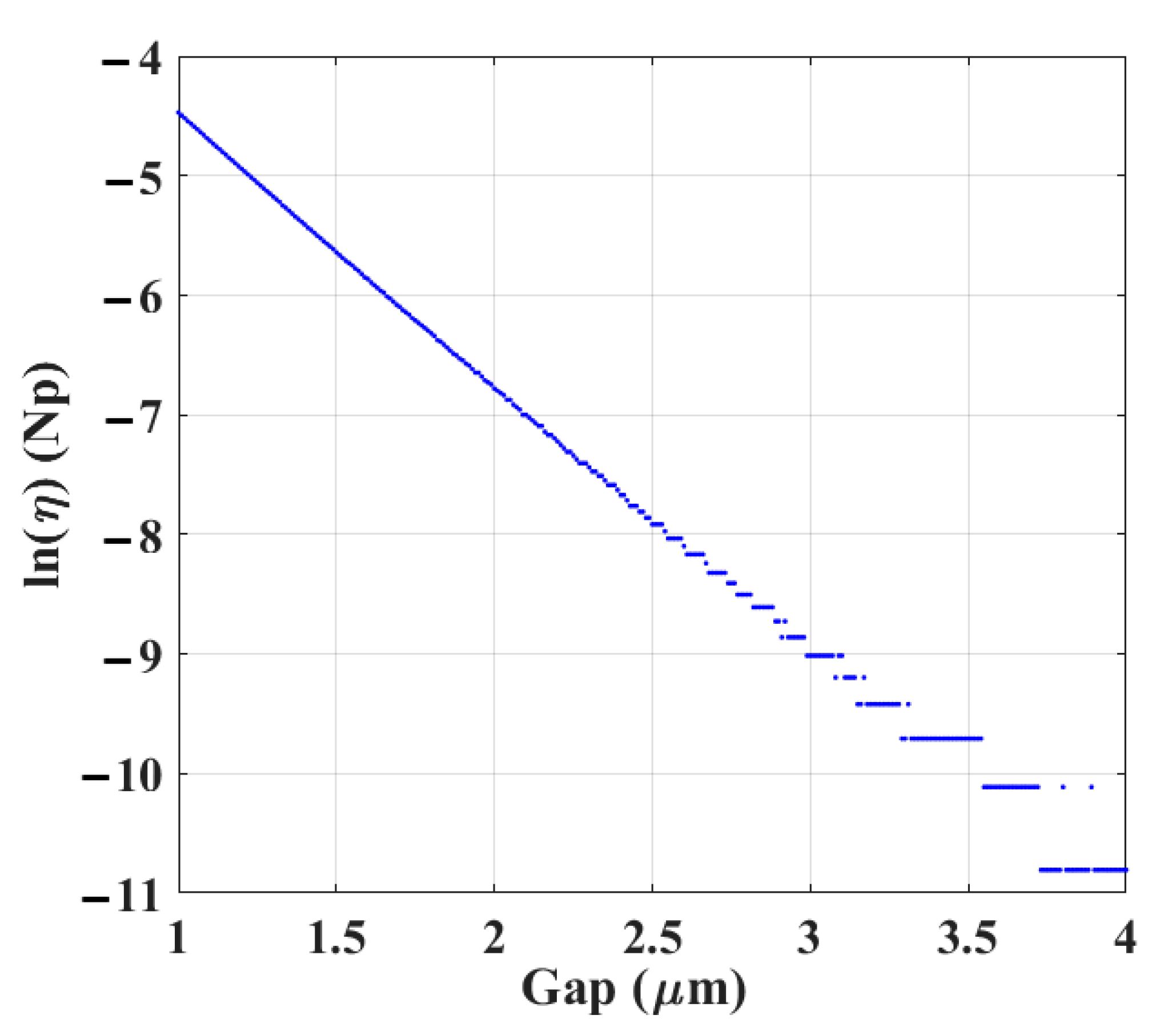
2.2. Dependence of Ring Resonator Coupling Coefficients on Gap

Two identical almost osculating circular rings separated by a small gap possess a mirror symmetry plane (say vertical) through the center of each ring and an orthogonal (say horizontal) plane through the midpoint between their centers. In the case of an individual ring resonator, the horizontal symmetry must be broken globally because the access guide must ultimately depart from a closed ring. However, that departure need only take place in a region of negligible coupling. The unitary transmission matrix K may then be taken as bisymmetric as follows:
K = exp i ν σ 1 = cos ν i sin ν i sin ν cos ν ;   det K = 1
where ν is a real scalar and:
σ 1 = 0 1 1 0
is the unique bisymmetric Pauli matrix.
The horizontal and vertical symmetry apply locally to a parallel pair of waveguides and ν in (14) may be considered a function of position along the optical axis. The modes of a pair of parallel waveguides treated as a single waveguide structure may be partitioned into a class of symmetric and a class of antisymmetric modes with respect to the horizontal mirror plane. When the waveguides are sufficiently separated, the lowest order symmetric and anti-symmetric modes are degenerate and can be constructed from a symmetric and antisymmetric linear superposition of the corresponding modes of the isolated waveguides. As the waveguides are brought closer together, the effective indices and the local field profiles begin to differ. In general, the antisymmetric mode acquires a lower effective index than the symmetric mode.
Assuming (14) applies locally, a vector basis is chosen so that the symmetric and antisymmetric modes correspond to the following:
S = 1 2 1 1   ;   A = 1 2 1 1
These vectors are the (orthonormal) eigenvectors of σ 1 with eigenvalues ± 1 and hence the following:
K S = exp i ν S K A = exp i ν A
For an adiabatic structure with no scattering to other local modes and slow evolution of the modal field profile as follows:
S z = exp i 0 z β S z d z S 0 A z = exp i 0 z β A z d z A 0
where β S and β A are the local wavenumber of the symmetric and antisymmetric modes. Consequently, up to a common phase factor, the evolution of the coupling is described by the following:
ν = 1 2 0 z β S z β A z d z ν = 0 z π λ 0 n e f f   S z n e f f   A z d z
where n e f f   S and n e f f   A are the effective indices of the symmetric and antisymmetric modes and λ 0 is the vacuum wavelength.
In the case of a circular ring with a straight access waveguide, the local gap x z is given by the following:
x z = x 0 + r 1 1 z r 2
where x 0 is the minimum gap at z = 0 and r is the outer radius of the ring. Above a certain minimum gap, to a good approximation the effective index split n e f f   S n e f f   A   falls exponentially as follows:
η = π λ 0 n e f f   S x n e f f   A x a exp b x
where the parameters a , b may be found by curve fitting effective index data provided by a mode solver. An extension of the integration range to ,   and the parabolic approximation x z x 0 + z 2 / 2 r permits an analytic integration of (19). The overall transmission of the interaction region is then given by (14) with the parameter ν given by the following:
ν a 2 π r / b exp b x 0

2.3. Quality Factor and Finesse

In the neighborhood of a resonant frequency ω 0 as follows:
b 1 / a 2 A 0 / 1 + i ω ω 0 / Δ ω
b 4 / a 2 B 0 / 1 + i ω ω 0 / Δ ω
where A 0 = κ 12 / Δ ω τ , B 0 = κ 43 κ 12 γ 2 / Δ ω τ , ω 0 τ = arg κ 11 κ 33 γ , and Δ ω τ = ln κ 11 κ 33 γ   . Here, Δ ω is the −3 dB half-bandwidth of the resonance, which may be related to the quality factor as follows:
Q = 1 2 ω 0 τ Δ ω τ 1 Q = 1 Q i n t + 1 Q e x t   ln γ 2   ω 0 τ + κ 12 2 + κ 34 2 ω 0 τ
The finesse may be expressed similarly as follows:
F = f FSR f 3 dB   = π 1 Δ ω τ 1 F = 1 F int + 1 F ext   ln γ 2   2 π + κ 12 2 + κ 34 2 2 π
Equations (25) and (26) show that quality factor and finesse approach their intrinsic value at the limit of no coupling to the external circuit and approach their extrinsic value at the limit of zero internal loss within the ring. The coupling of an ultra-low loss ring to the external circuit must be very weak to not compromise (load) the intrinsic (unloaded) Q or   F .
If the internal loss is negligible ( γ 1 ) compared to the out-coupling to the external circuit, then for a ring with identical couplers, the on-resonance transmission is as follows:
b 1 / a 2 2 κ 12 κ 12 2 + κ 34 2 1 / κ 12   ;   κ 34 = κ 12
b 4 / a 2 2 κ 12 κ 34 κ 12 2 + κ 34 2 1 ;   κ 34 = κ 12
The field amplitude within the ring scales in inverse proportion to the magnitude of the cross-coupling coefficient κ 12   and the threshold for the onset of nonlinear optical effects reduces commensurately. In the two identical lossless coupler cases, the on-resonance transmission is unity, consistent with energy conservation.

3. Fabrication and Experimental Setup

The spectrometer architecture uses a tunable ring resonator as a scanning fine filter. To realize a system demonstration, ring resonators operating over the entire C-band with 1 GHz bandwidth resonances tunable over a free spectral range (FSR) of 50 GHz are required. The bandwidth depends on the cross-coupled power only if the excess loss per turn is negligible compared to the out-coupled power per turn. Consequently, the spectrometer resolution is limited by the ring excess loss per turn. Hence, fabrication on an integration platform supporting low-loss straight guides and bends, low dispersion, and a mature phase shifter technology is paramount.
To demonstrate a readily manufacturable system, a commercially accessible foundry with a mature process should be selected. The CMOS-compatible TriPleX™ waveguide technology offered by LioniX International has been chosen for test-structure fabrication, which includes several ring resonators designed to meet the requirements. Their Multi Project Wafer run (MPW) process supports only the asymmetric double strip (ADS) waveguide, which, consequently, is taken as the reference waveguide for all test-structure designs. The TriPleX™ ADS waveguide, operating at the telecom wavelength (1.55 μm), offers low propagation and bending loss with high modal birefringence [32,38]. The MPW default waveguide width and minimum feature size are 1.1 μm and 1 μm, respectively. The aspect ratio of the waveguide follows the standard configuration for the ADS technology given in [38]. Figure 2a depicts the transverse mode profile of the fundamental TE mode simulated by the mode solver Fimmwave. The ‘W’ represents the top width of the top stripe of the ADS waveguide. In Figure 2a, ‘W’ is equal to the default width. An etching angle of 82°, given in [38], is also applied for the construction of the waveguide in the simulation platform, which results in a very close estimation of effective index and group index via Fimmwave simulation when compared with their equivalents provided by LioniX International. Figure 2b,c shows the variation of effective indices and group indices with ‘W’. It can be observed that for the default width adopted in the MPW process, simulation results indicate only the propagation of TE00 and TM00 modes through the straight waveguide. The straight waveguide loss of the TE00 mode is ≤0.5 dB/cm, as specified by LioniX International. The TM polarization has a much larger propagation loss and bending loss and is therefore not supported. To facilitate optical characterization, the chip is pigtailed using polarization-maintaining fiber (PMF) arrays and wire bonded.
Several add-drop ring resonators have been fabricated, as shown in Figure 3. Each RR follows a circular geometry with straight access guides to equip the coupling region. A 50 GHz FSR requirement fixes the radius of the rings to be 537 μm. Each ring is equipped with a thermo-optic phase shifter, as shown in Figure 3a. The proposed design rule has been applied to specify the minimum gap between the ring waveguide and access waveguide at the curved coupling section for a given power cross-coupling ratio. Consequently, the RR test-structure variations will differ in performance. Figure 3a depicts four types of circular ring resonators with identical radii and variable gaps. The gaps are chosen to be 1.2 μm (RR1), 1.5 μm (RR2), 1.8 μm (RR3-RR4), and 2 μm (RR5—not shown in Figure 3a) to enable an assessment of the utility of the design rule. Each variant operates over the whole C band. Figure 3b shows the measured transmission spectrum of the RR1. A tunable laser (Agilent 81680A) capable of tuning over the whole C-band is utilized for characterizing the ring resonators. A polarization controller is utilized to maximize TE mode transmission. The input power to the device under test (DUT) is 0 dBm. The output is detected by an optical power sensor (Agilent 81632A) and analyzed by a lightwave measurement system (Agilent 8164A). It can be observed that resonant peak transmission at the drop port of the ring is almost constant at −5 dBm over the whole C band. The optical loss includes the pigtailed fiber-chip coupling losses, which can be estimated individually by using the alignment loop waveguides present in the chip. Each access waveguide is terminated by an integrated spot size converter (SSC) at the end facets of the chip.

4. Discussion

Figure 4a,b shows the tuning behavior of the fabricated ring resonators. A DC voltage is applied to the integrated phase shifters and the corresponding current is recorded. A tuning over the complete FSR can be achieved with a variation of the applied power from 0 mW to ~500 mW. Figure 4a depicts the drop path transmission spectra of RR1, which shows the shift of the resonant frequency over one FSR. Similar tuning behavior is observed for RR2, RR3, and RR5, which use an identical phase shifter configuration and thus provide similar linear I-V characteristics corresponding to a heater resistance of ~735 Ω. RR4 uses a phase shifter, which is shorter in length and, thus, has a lower resistance of ~375 Ω. Figure 4b shows that a similar linear dependence between the resonant wavelength shift and applied power is maintained for all phase shifter configurations.
To investigate the evolution of FSR over a larger wavelength span, it is mandatory to have finely sampled transmission spectra. The coarser sampling necessary due to instrument limitations to accommodate a large band may result in the extraction of a local FSR that is subject to errors that mask small changes to dispersion. An attempt to observe the evolution of FSR over the 1540–1560 nm span from the transmission spectra and isolate the effect of dispersion on it is presented in Figure 4c. The x-axis indexes the sequence of resonant peaks observed in the measured data, and their corresponding frequencies relative to a reference frequency are plotted. The reference frequencies for RR1, RR3, RR4, and RR5 are 193.4863, 193.4878, 193.4446, and 193.4678 THz, respectively. A linear fit has been achieved for all ring resonators with a noise-like residual with a root mean squared magnitude of 0.3536, 0.3489, 0.3673, and 0.3611 GHz for RR1, RR3, RR4, and RR5, respectively. To investigate the effect of coarser sampling on the validity of linear fitting, drop and through transmissions of the individual ring are measured over different wavelength spans with different resolutions at different times, and almost identical fitting has been observed. Quadratic fitting with the least squares method over these resonant frequencies over the corresponding span reveals a very small contribution of dispersion in the FSR evolution with wavelength, which is also evident from the linear fit.
The design and optimization of a ring resonator compliant with the specified bandwidth and FSR are challenging. Available computational methods seem inadequate (inefficient or inaccurate) for the task of predicting the dimensions of compliant designs. The FSR requirement and the choice of an integration platform and waveguide technology set the ring shape/diameter. The bandwidth depends on the cross-coupled power, which is controlled by the gap between the ring waveguide and access waveguide. Based on the quasi-analytic eigenmode expansion (EME) method presented in Section 2.2, a design rule to calculate the optimum gap to achieve the desired power cross-coupling ratio involves the following steps:
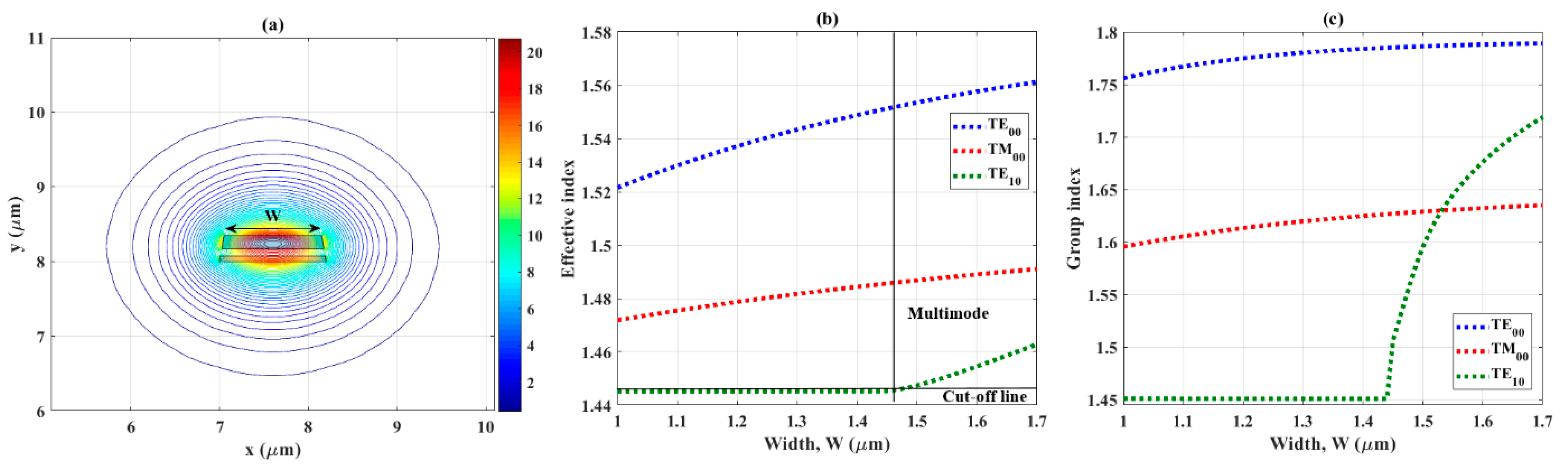
  • The effective index split of the two lowest-order local modes is found using a mode solver. The accuracy may be improved by increasing the number of local modes in the interaction;
  • The difference data may be fitted to a suitable curve by a curve fitting toolbox. For an adiabatic curved coupler, the dependence of the effective index difference as a function of z is certainly a smooth bell-shaped curve, as in (21);
  • The fitting will aid its numerical integration. If the asymptotic tails decay exponentially, it will allow an analytic integration of the tail region for l . This will predict the overall power transfer matrix of the couplers based on proximate curved waveguides.
Photon design offers a fully vectorial mode solver tool for 2D+Z waveguide structures such as Fimmwave, which is used to inform the quasi-analytic adiabatic EME method. The ADS waveguide is designed to propagate the fundamental TE mode efficiently. Fundamental symmetric and antisymmetric local eigenmodes for TE polarization have been investigated. It can be observed from Figure 5 that ln( ν ) and the minimum gap at the coupling region of the RR follow a linear relationship over the range of the gaps investigated in this report. In [31], OptiBPM has been utilized to scan the power cross-coupling ratio and, although outside its domain of validity, it predicted a similar coupling ratio for the same range of gaps.
To validate the design rule and determine the optimum gap needed to satisfy the FSR and bandwidth requirement, the parameter extraction method described in Section 2.1 is applied to the measured add-drop ring resonator transmission data. A separate experiment with a Mach–Zehnder delay interferometer (MZDI) test structure on the same chip adjacent to the rings confirmed that couplers with the same design on the same chip are essentially identical, which can also be concluded for the add- and drop-couplers of a ring resonator.
The periodic complex transmission spectrum of a ring resonator may be modeled by a simple rational trigonometrical polynomial that has one zero and one pole as discussed in Section 2.1. The intensity transmission expressed similarly maps the zero and pole to a reciprocal conjugate zero pair and a reciprocal conjugate pole pair respectively. There is consequently an ambiguity when fitting intensity data in the correct location of the pole and zero. In the case of a passive ring, the pole must be located inside the unit circle for reasons of stability, but either of the two zero positions is valid. This ambiguity is resolved under the assumption of identical add-drop couplers as the zero location is equal to the ring loss γ and consequently inside the unit circle.
A good fit to the measured data, especially at the peak and notch of the drop path and through path transmission, is necessary to disentangle loss and coupling coefficients. Good fits have been achieved at the resonant peaks and notches for all rings, although departure at high extinction can be observed due to the noise floor of the measurement. Figure 6 shows the fitted spectra of drop- and through-path transmission alongside the measured data for RR1, RR2, and RR3.
A list of extracted parameters from measured and fitted data is given in Table 1. The design FSR for all fabricated rings is the same. Table 1 shows that the measured FSRs for all rings lie within ~49.4–49.8 GHz, except RR5, which has a smaller FSR of ~46.55 GHz. Sub-GHz bandwidth cannot be achieved for RR1. The loss γ can be disentangled further into intrinsic ring waveguide loss and extrinsic coupler excess loss if the propagation and bending losses established by the process are known. LioniX International guarantees a straight waveguide loss <0.5 dB/cm with a typical value of ~0.2 dB/cm and negligible bending loss for its TriPleX™ ADS MPW process and lower waveguide loss for a dedicated run using stepper lithography. The losses extracted for RR1 and RR2 reveal that the straight waveguide loss is well below the upper limit. The loss also increases with the gap. These observations suggest a better waveguide loss figure has been achieved in the MPW run, and the fabricated ring coupler suffers from non-zero excess loss increasing with a gap. The excess loss per coupler is estimated on the basis of a straight waveguide loss of 0.2 dB/cm and negligible bending loss, which results in the maximum excess loss per coupler as follows: ~0.025 dB, ~0.05 dB, ~0.06 dB, ~0.085 dB, and ~0.055 dB for RR1, RR2, RR3, RR4, and RR5 respectively.
One possible reason for the excess loss is due to the waveguide wall roughness within the coupling region. The fiber-chip coupling loss, including the loss due to the SSC at each facet, is measured as ~1.675 dB by measuring the transmission of light in alignment loop waveguides. A very small discrepancy in the measured fiber-chip coupling loss is observed for different alignment loop waveguides located on different edges of the chip, which suggests a <1% experimental/fitting uncertainty. This uncertainty might be the reason for the lower loss of RR5 than that of RR3, as RR5 is located in a different location than the rest of the rings. The outlier is RR4. The loss for RR4 is higher than RR3 with the same coupler configuration, which suggests the additional loss and thus larger bandwidth is a consequence of the different phase shifter geometry. The geometries differ in length only as shown in Figure 3a; RR3 has a phase shifter with a length of 2577.4 μm, whereas the phase shifter of RR4 has a length of 1265.3 μm. Each phase shifter is formed by the Cr heater with Cr/Au electrical leads.
Figure 7 provides a comparison between the estimated power cross-coupling ratio derived by the proposed quasi-analytic EME method and the power cross-coupling parameters extracted from transmission data through the proposed extraction method. A good match can be observed between the measured and predicted data. The LioniX International MPW process used as specified could result in a ±200 nm uncertainty in the fabricated gap. The measured coefficient of RR2 shows the largest deviation from its predicted coupling coefficient. A match between the measured coupling parameter for RR2 and its corresponding gap from the prediction results in a gap of ~1.2429 μm instead of 1.2 μm. The difference is ~42.9 nm, which suggests that measurement points are well within the error bars due to fabrication uncertainty. LioniX International confirms that from 2022, the MPW process will be updated to the stepper lithography used for dedicated runs, which will substantially improve the loss and dimension uncertainty of the MPW process.

5. Conclusions

In summary, a design rule for determining the gap at the coupling region and a parameter extraction method are proposed and implemented in designing and investigating the spectral characteristics of fabricated ring resonators. The design rule employs a quasi-analytic eigenmode expansion (EME) method, which is simple, fast, and less computationally resource-hungry compared to other simulation schemes in designing sub-GHz bandwidth-50 GHz range FSR ring resonators. These strict specifications are crucial for a sub-GHz resolution, wideband, panoramic spectral sensing application. Several ring resonators based on the design rule estimation have been fabricated on a Si3N4 platform using an MPW process. A very good match between the predicted and measured coupling behavior has been found for all rings. The results suggest a ring resonator with a gap between 1.2 and 1.5 μm can meet the tight specifications perfectly while maintaining less loss. The parameter extraction method used to validate the design procedure is a single resonance-based method, which only needs intensity data from the through- and drop-path of the rings to disentangle the loss and coupling coefficients. The associated data analysis, with the assumptions of identical add- and drop couplers with adiabatic mode evolution, can solve the phase problem, which convolutes the separation of these parameters. The proposed method retrieves the complex transmission from an intensity-only measurement. The design rule and parameter extraction method can be adapted to other material platforms.

Author Contributions

Conceptualization, G.M.H. and T.J.H.; methodology, G.M.H. and T.J.H.; software, G.M.H., M.H. and T.J.H.; validation, G.M.H., H.G. and T.J.H.; formal analysis, G.M.H., P.L. and T.J.H.; investigation, G.M.H., M.H. and P.L.; resources, G.M.H.; data curation, G.M.H.; writing—original draft preparation, G.M.H. and T.J.H.; writing—review and editing, P.L., M.R., E.B. and T.J.H.; visualization, G.M.H.; supervision, T.J.H.; project administration, T.J.H. and M.R. All authors have read and agreed to the published version of the manuscript.

Funding

This research received no external funding.

Institutional Review Board Statement

Not applicable.

Informed Consent Statement

Not applicable.

Data Availability Statement

The data that supports the findings of this study are available from the corresponding author upon reasonable request.

Acknowledgments

The authors acknowledge Huawei Technologies Canada for their support through a project contract. The authors also acknowledge the software related support from CMC Microsystems. Trevor J. Hall is grateful to the University of Ottawa for their support of a University Research Chair. Gazi Mahamud Hasan acknowledges Ontario Student Assistance Program for their support through the Ontario Graduate Scholarship. Gazi Mahamud Hasan is also grateful to the University of Ottawa for their support through International Admission Scholarship.

Conflicts of Interest

The authors declare no conflict of interest.

References

  1. Bogaerts, W.; Dumon, P.; Thourhout, D.V.; Taillaert, D.; Jaenen, P.; Wouters, J.; Beckx, S.; Wiaux, V.; Baets, R.G. Compact wavelength-selective functions in silicon-on-insulator photonic wires. IEEE J. Sel. Top. Quantum Electron. 2006, 12, 1394–1401. [Google Scholar] [CrossRef]
  2. Antonacci, G.; Elsayad, K.; Polli, D. On-Chip Notch Filter on a Silicon Nitride Ring Resonator for Brillouin Spectroscopy. ACS Photonics 2022, 9, 772–777. [Google Scholar] [CrossRef]
  3. Xia, F.; Sekaric, L.; Vlasov, Y. Ultracompact optical buffers on a silicon chip. Nat. Photonics 2007, 1, 65–71. [Google Scholar] [CrossRef]
  4. Ibrahim, T.; Grover, A.R.; Kuo, L.C.; Kanakaraju, S.; Calhoun, L.C.; Ho, P.T. All-optical AND/NAND logic gates using semiconductor microresonators. IEEE Photon. Technol. 2003, 15, 1422–1424. [Google Scholar] [CrossRef]
  5. Ji, R.; Yang, L.; Zhang, L.; Tian, Y.; Ding, J.; Chen, H.; Lu, Y.; Zhou, P.; Zhu, W. Microring-resonator-based four-port optical router for photonic networks-on-chip. Opt. Express 2011, 19, 18945–18955. [Google Scholar] [CrossRef]
  6. Fan, X.; White, I.M.; Zhu, H.; Suter, J.D.; Oveys, H. Overview of novel integrated optical ring resonator bio/chemical sensors. In Proceedings of the SPIE Laser Resonators Beam Control IX, San Jose, CA, USA, 14 February 2007. [Google Scholar]
  7. Xu, Q.; Manipatruni, S.; Schmidt, B.; Shakya, J.; Lipson, M. 12.5 Gbit/s carrier-injection-based silicon micro-ring silicon modulators. Opt. Express 2007, 15, 430–436. [Google Scholar] [CrossRef]
  8. Jin, W.; Yang, Q.F.; Chang, L.; Shen, B.; Wang, H.; Leal, M.A.; Wu, L.; Gao, M.; Feshali, A.; Paniccia, M.; et al. Hertz-linewidth semiconductor lasers using CMOS-ready ultra-high-Q microresonators. Nat. Photonics 2021, 15, 346–353. [Google Scholar] [CrossRef]
  9. Ye, Z.; Twayana, K.; Andrekson, P.A. High-Q Si3N4 microresonators based on a subtractive processing for Kerr nonlinear optics. Opt. Express 2019, 27, 35719–35727. [Google Scholar] [CrossRef]
  10. Bogaerts, W.; Heyn, P.D.; Vaerenbergh, T.V.; Vos, K.D.; Selvaraja, S.K.; Claes, T.; Dumon, P.; Bienstman, P.; Thourhout, D.V.; Baets, R. Silicon microring resonators. Laser Photonics Rev. 2012, 6, 47–73. [Google Scholar] [CrossRef]
  11. Mahmoud, M.; Cai, L.; Bottenfield, C.; Piazza, G. Lithium niobate electro-optic racetrack modulator etched in Y-cut LNOI platform. IEEE Photon. J. 2018, 10, 1–10. [Google Scholar] [CrossRef]
  12. Chen, L.; Wood, M.G.; Reano, R.M. 12.5 pm/V hybrid silicon and lithium niobate optical microring resonator with integrated electrodes. Opt. Express 2013, 21, 27003–27010. [Google Scholar] [CrossRef] [PubMed]
  13. Ahmed, A.N.R.; Shi, S.; Zablocki, M.; Yao, P.; Prather, D.W. Tunable hybrid silicon nitride and thin-film lithium niobate electro-optic microresonator. Opt. Lett. 2019, 44, 618–621. [Google Scholar] [CrossRef] [PubMed]
  14. Grover, R.; Absil, P.P.; Van, V.; Hryniewicz, J.V.; Little, B.E.; King, O.; Calhoun, L.C.; Johnson, F.G.; Ho, P.T. Vertically coupled GaInAsP–InP microring resonators. Opt. Lett. 2001, 26, 506–508. [Google Scholar] [CrossRef] [PubMed]
  15. Ibrahim, T.A.; Van, V.; Ho, P.T. All-optical time-division demultiplexing and spatial pulse routing with a GaAs/AlGaAs microring resonator. Opt. Lett. 2002, 27, 803–805. [Google Scholar] [CrossRef] [PubMed]
  16. Bogaerts, W.; Bienstman, P.; Baets, R. Scattering at sidewall roughness in photonic crystal slabs. Opt. Lett. 2003, 28, 689–691. [Google Scholar] [CrossRef]
  17. Spencer, D.T.; Bauters, J.F.; Heck, M.J.; Bowers, J.E. Integrated waveguide coupled Si3N4 resonators in the ultrahigh-Q regime. Optica 2014, 1, 153–157. [Google Scholar] [CrossRef]
  18. Puckett, M.W.; Liu, K.; Chauhan, N.; Zhao, Q.; Jin, N.; Cheng, H.; Wu, J.; Behunin, R.O.; Rakich, P.T.; Nelson, K.D.; et al. 422 Million intrinsic quality factor planar integrated all-waveguide resonator with sub-MHz linewidth. Nat. Commun. 2021, 12, 1–8. [Google Scholar]
  19. Liu, K.; Jin, N.; Cheng, H.; Chauhan, N.; Puckett, M.W.; Nelson, K.D.; Behunin, R.O.; Rakich, P.T.; Blumenthal, D.J. Ultralow 0.034 dB/m loss wafer-scale integrated photonics realizing 720 million Q and 380 μW threshold Brillouin lasing. Opt. Lett. 2022, 47, 1855–1858. [Google Scholar] [CrossRef]
  20. Ciminelli, C.; Innone, F.; Brunetti, G.; Conteduca, D.; Dell’Olio, F.; Tatoli, T.; Armenise, M.N. Rigorous model for the design of ultra-high Q-factor resonant cavities. In Proceedings of the 18th International Conference on Transparent Optical Networks (ICTON), Trento, Italy, 10–14 July 2016. [Google Scholar]
  21. Lu, X.; McClung, A.; Srinivasan, K. High-Q slow light and its localization in a photonic crystal microring. Nat. Photonics 2022, 16, 66–71. [Google Scholar] [CrossRef]
  22. Kyotoku, B.B.; Chen, L.; Lipson, M. Sub-nm resolution cavity enhanced micro-spectrometer. Opt. Express 2010, 18, 102–107. [Google Scholar] [CrossRef]
  23. Yurtsever, G.; Baets, R. Integrated spectrometer on silicon on insulator. In Proceedings of the 16th Annual Symposium of the IEEE Photonics Benelux Chapter, Ghent, Belgium, 1–2 December 2011. [Google Scholar]
  24. Xia, Z.; Eftekhar, A.A.; Soltani, M.; Momeni, B.; Li, Q.; Chamanzar, M.; Yegnanarayanan, S.; Adibi, A. High resolution on-chip spectroscopy based on miniaturized microdonut resonators. Opt. Express 2011, 19, 12356–12364. [Google Scholar] [CrossRef] [PubMed]
  25. Xiang, C.; Morton, P.A.; Khurgin, J.; Morton, C.; Bowers, J.E. Widely tunable Si3N4 triple-ring and quad-ring resonator laser reflectors and filters. In Proceedings of the 2018 IEEE 15th International Conference on Group IV Photonics (GFP), Cancun, Mexico, 29–31 August 2018. [Google Scholar]
  26. Zheng, S.; Cai, H.; Song, J.; Zou, J.; Liu, P.Y.; Lin, Z.; Kwong, D.-L.; Liu, A.-Q. A Single-Chip Integrated Spectrometer via Tunable Microring Resonator Array. IEEE Photon. J. 2019, 11, 1–9. [Google Scholar] [CrossRef]
  27. Zheng, S.N.; Zou, J.; Cai, H.; Song, J.F.; Chin, L.K.; Liu, P.Y.; Lin, Z.P.; Kwong, D.L.; Liu, A.Q. Microring resonator-assisted Fourier transform spectrometer with enhanced resolution and large bandwidth in single chip solution. Nat. Commun. 2019, 10, 1–8. [Google Scholar] [CrossRef] [PubMed]
  28. Li, Y.; Li, J.; Yu, H.; Yu, H.; Chen, H.; Yang, S.; Chen, M. On-chip photonic microsystem for optical signal processing based on silicon and silicon nitride platforms. Adv. Opt. Technol. 2018, 7, 81–101. [Google Scholar] [CrossRef]
  29. Kita, D.M.; Lin, H.; Agarwal, A.; Richardson, K.; Luzinov, I.; Gu, T.; Hu, J. On-chip infrared spectroscopic sensing: Redefining the benefits of scaling. IEEE J. Sel. Top. Quantum Electron. 2016, 23, 340–349. [Google Scholar] [CrossRef]
  30. Hasan, M.; Rad, M.; Hasan, G.M.; Liu, P.; Dumais, P.; Bernier, E.; Hall, T.J. Ultra-high resolution wideband On-chip spectrometer. IEEE Photon. J. 2020, 12, 1–17. [Google Scholar] [CrossRef]
  31. Hasan, M.; Hasan, G.M.; Ghorbani, H.; Rad, M.; Liu, P.; Bernier, E.; Hall, T. Circuit design and integration feasibility of a high-resolution broadband on-chip spectral monitor. arXiv 2021, arXiv:2108.10121. [Google Scholar]
  32. Zhuang, L.; Marpaung, D.; Burla, M.; Beeker, W.; Leinse, A.; Roeloffzen, C. Low-loss, high-index-contrast Si3N4/SiO2 optical waveguides for optical delay lines in microwave photonics signal processing. Opt. Express 2011, 19, 23162–23170. [Google Scholar] [CrossRef]
  33. Yariv, A. Universal relations for coupling of optical power between microresonators and dielectric waveguides. Electron. Lett. 2000, 36, 321–322. [Google Scholar] [CrossRef]
  34. Gifford, D.K.; Soller, B.J.; Wolfe, M.S.; Froggatt, M.E. Optical vector network analyzer for single-scan measurements of loss, group delay, and polarization mode dispersion. Appl. Opt. 2005, 44, 7282–7286. [Google Scholar] [CrossRef]
  35. Heebner, J.E.; Wong, V.; Schweinsberg, A.; Boyd, R.W.; Jackson, D.J. Optical transmission characteristics of fiber ring resonators. IEEE J. Quantum Electron. 2004, 40, 726–730. [Google Scholar] [CrossRef]
  36. Matres, J.; Ballesteros, G.C.; Mas, S.; Brimont, A.; Sanchis, P.; Marti, J.; Oton, C.J. Optical phase characterization of photonic integrated devices. IEEE J. Sel. Top. Quantum Electron. 2013, 20, 417–421. [Google Scholar] [CrossRef]
  37. McKinnon, W.R.; Xu, D.-X.; Storey, C.; Post, E.; Densmore, A.; Delâge, A.; Waldron, P.; Schmid, J.H.; Janz, S. Extracting coupling and loss coefficients from a ring resonator. Opt. Express 2009, 17, 18971–18982. [Google Scholar] [CrossRef] [PubMed]
  38. Roeloffzen, C.G.H.; Hoekman, M.; Klein, E.J.; Wevers, L.S.; Timens, R.B.; Marchenko, D.; Geskus, D.; Dekker, R.; Alippi, A.; Grootjans, R.; et al. Low-loss Si3N4 TriPleX optical waveguides: Technology and applications overview. IEEE J. Sel. Top. Quantum Electron. 2018, 24, 1–21. [Google Scholar] [CrossRef] [Green Version]
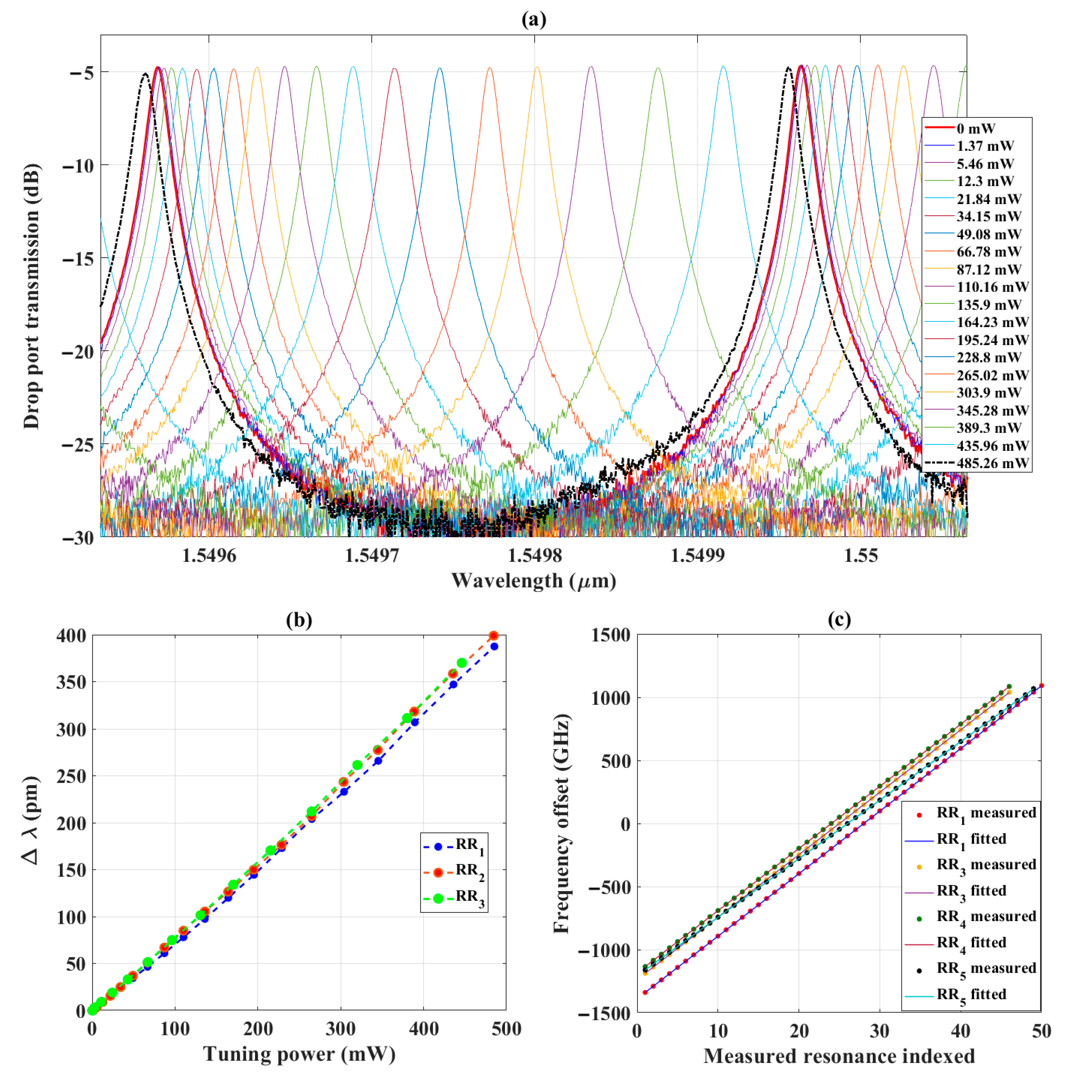
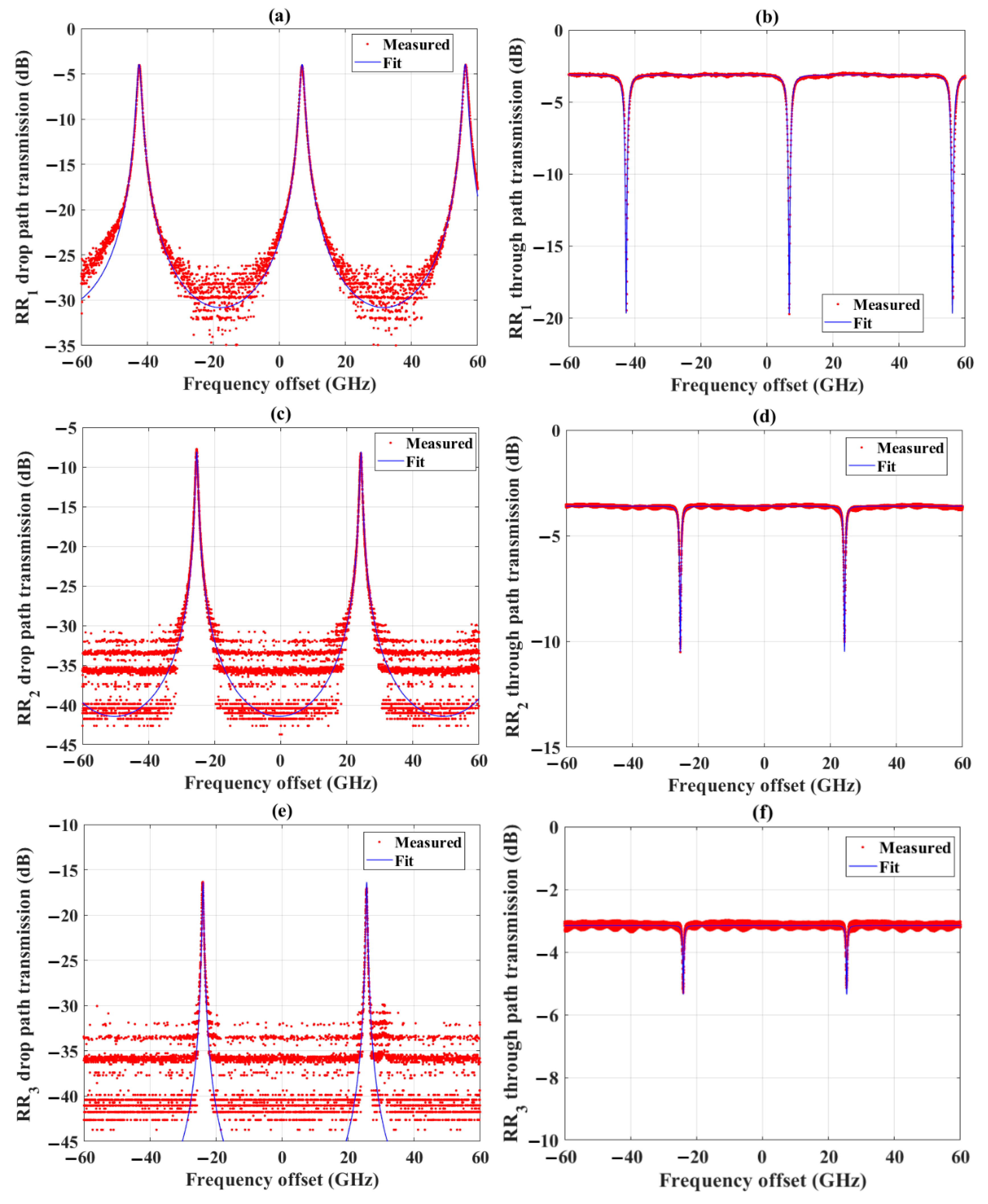
Figure 1. Model of a ring resonator with transmission and coupling coefficients.
Photonics 09 00651 g001
Figure 2. (a) Simulated transversal profile of the major electric field component Ex of the TE00 mode of the ADS waveguide, W = 1.1 μm is the top-width of the top stripe; (b) effective index variation, and (c) group index variation of first three modes with the width (W) of the waveguide.
Photonics 09 00651 g002
Figure 3. (a) Micrograph of different ring resonators. Each RR has the same radius, but different gaps. The minimum gaps of the ring waveguide and access waveguide are 1.2 μm, 1.5 μm, and 1.8 μm for RR1, RR2, RR3, and RR4, respectively. All rings are equipped with thermo-optic phase shifter heating elements, which cover almost the whole circumference of the ring waveguide except RR4, which covers less than half of the circumference; (b) measured drop path transmission spectrum of the RR1 over the whole C band.
Photonics 09 00651 g003
Figure 4. (a) Tuning spectra of RR1 for different thermo-optic phase shifter applied voltage, (b) resonant wavelength shifts of RR1, RR2, and RR4 as a function of heater power, and (c) linear fit to the multiplicity of resonant frequencies for RR1, RR3, RR4, and RR5.
Photonics 09 00651 g004
Figure 5. Natural logarithm of the integrand η (μm−1) from (21) vs. gap.
Photonics 09 00651 g005
Figure 6. Drop- and through-path transmission spectra for (a,b) RR1, (c,d) RR2, and (e,f) RR3. The measurements have been taken with 0.1 pm resolution using the abovementioned experimental setup. The reference frequency is 193.414 THz (1550 nm).
Photonics 09 00651 g006
Figure 7. Cross power coupling ratio vs. gap.
Photonics 09 00651 g007
Table 1. Measured and extracted parameters of fabricated ring resonators.
Gap (μm)FWHM Bandwidth (GHz)FSR (GHz)Cross-Power Coupling Ratio (%)Ring Transmission Loss (dB)Quality Factor, Q
RR11.2~1.43~49.47.460.12135,258
RR21.5~0.68~49.72.330.17284,469
RR31.8~0.45~49.550.640.19429,867
RR41.8~0.55~49.80.680.24351,671
RR52.0~0.35~46.550.290.18552,640
Publisher’s Note: MDPI stays neutral with regard to jurisdictional claims in published maps and institutional affiliations.

