Article

Introducing Corrections to the Reflectance of Graphene by Light Emission

by
Ken-ichi Sasaki
1,*,†,
Kenichi Hitachi
2,†,
Masahiro Kamada
3,†,
Takamoto Yokosawa
3,†,
Taisuke Ochi
3,† and
Tomohiro Matsui
3,†
1
NTT Research Center for Theoretical Quantum Physics and NTT Basic Research Laboratories, NTT Corporation, 3-1 Morinosato Wakamiya, Atsugi 243-0198, Kanagawa, Japan
2
NTT Basic Research Laboratories, NTT Corporation, 3-1 Morinosato Wakamiya, Atsugi 243-0198, Kanagawa, Japan
3
Advanced Research Laboratory, Anritsu Corporation, 5-1-1 Onna, Atsugi 243-8555, Kanagawa, Japan
*
Author to whom correspondence should be addressed.
These authors contributed equally to this work.
Submission received: 15 January 2024 / Revised: 26 January 2024 / Accepted: 13 February 2024 / Published: 15 February 2024
(This article belongs to the Section Carbon Materials and Carbon Allotropes)

Abstract

:
Monolayer graphene absorbs 2.3 percent of the incident visible light. This “small” absorption has been used to emphasize the visual transparency of graphene, but it in fact means that multilayer graphene absorbs a sizable fraction of incident light, which causes non-negligible fluorescence. In this paper, we formulate the light emission properties of multilayer graphene composed of tens to hundreds of layers using a transfer matrix method and confirm the method’s validity experimentally. We quantitatively explain the measured contrasts of multilayer graphene on SiO2/Si substrates and find sizable corrections, which cannot be classified as incoherent light emissions, to the reflectance of visible light. The new component originates from coherent emission caused by absorption at each graphene layer. Multilayer graphene thus functions as a partial coherent light source of various wavelengths, and it may have surface-emitting laser applications.

Graphical Abstract

1. Introduction

The visual detection of graphene on Si substrates involves a complex scientific aspect related to the interference effects of light [1,2,3]. To enhance visibility, it is crucial for the contrast between the reflectances from the substrate and the graphene layer to be sufficiently large. Si substrates with a specific thickness of SiO 2 ( d SiO 2 ) are known to provide advantages in this context [4,5]. Specifically, when the optical path length difference of the SiO 2 layer is one-half or three-half the wavelength of the incident light, the contrast reaches its maximum.
The enhanced visibility of graphene is primarily attributed to a substrate-induced enhancement of light absorption. This enhancement is valuable not only for graphene detection but also for exploring notable phenomena. For instance, the reflectance of specific graphene multilayers on SiO2/Si substrates can be reduced to zero for normally incident visible light with a wavelength ( λ ) approximately equal to 2 d SiO 2 . Zero reflectance is achieved through destructive interference caused by SiO 2 and a significant absorption coefficient of graphene [6,7,8]. More importantly, the reflectance of multilayer graphene on SiO2/Si substrates is intricately determined because the significant absorption may result in non-negligible luminescence. This luminescence also functions as a secondary light source, leading to more sophisticated interference effects of light [9,10,11,12,13,14,15].
Since graphene lacks an energy bandgap, unlike semiconductors, it is naturally expected that the impact of light emission on its optical properties is negligible. However, electrons that have absorbed light undergo various relaxation processes towards the ground state [16,17], generally involving luminescence contributions. For instance, Lui et al. [12] and Suemoto et al. [14] reported that graphene and graphite emit light under femtosecond laser pulse excitation, respectively. In this paper, we demonstrate that, despite the tiny branching ratio of light emission to absorption, light emission constitutes the primary correction to visible reflectance due to the substantial absorption of graphene. We find this notable feature for the first time by leveraging both the destructive interference effects of substrates and the coherence of the multilayer structure. Additionally, we show that light emission significantly contributes to enhancing the visibility of graphene on a substrate.
In this study, we delineate coherent and incoherent corrections to the reflectance of multilayer graphene (on SiO2/Si substrates) caused by the light it emits after absorbing incident light. The coherent corrections are dependent on only two parameters: the branching ratio ( B ) of coherent light emission to absorbed light and the phase (+ or −) of the emitted light. Both parameters are assumed to be independent of the number of layers (N) and the wavelength of light. Contrasts (reflectivities) calculated using these phenomenologically determined parameters show reasonable agreement with measured values for various N. Despite the branching ratio, determining the strength of light emitted from a graphene monolayer, which is less than one percent, the coherent components become the primary corrections to the reflectance of multilayer graphene. This is due to coherence increasing the amplitude of reflection through constructive interference. Furthermore, based on the observation that the phase of reflection and transmission coefficients of each layer translates into the amplitude of the emitted light, we hypothesize that the origin of the coherent components is coherent light emission stimulated by the incident light. Meanwhile, the Raman effect is explained as incoherent corrections. These conclusions are independent of the specific values of the two parameters.
Recently, the optical constants of single-layer graphene were measured with high accuracy [18,19]. However, classical electromagnetic models were employed for fitting and interpreting the results. Our approach advances the physical understanding of the measured optical constants of single-layer graphene to a more fundamental level, incorporating principles of quantum electrodynamics that describe the creation of photons (light emission). Moreover, our formulation is versatile and generally applicable to any layered material and superlattice, promising an accurate description of their optical processes.
Multilayer graphene composed of tens to hundreds of layers is an interesting research subject. However, it has not been explored much, partly because the success of the exfoliation method has rapidly shifted the interest of many researchers from infinite layers of graphite to few-layer graphene. The obvious advantage of multilayer graphene is that it can increase signal strength [20], whereas the signal strength of few-layer graphene is low and difficult to measure. Besides that, multilayer graphene hosts various intriguing phenomena. For instance, studies have revealed that the optimal number of layers for absorbing infrared radiation is 87 [21]. Additionally, a notable nonlinear optical effect has been attributed to multilayer graphene [22,23,24]. Yang et al., for instance, demonstrated the maximum third-harmonic signal from 24-layer graphene on a quartz substrate [25].
This paper is structured as follows: In Section 2, we present fundamental insights into the reflectance of multilayer graphene on SiO2/Si substrates. By utilizing the Fresnel equation, we can replicate measured contrasts and assert that the optical constants obtained by El-Sayed et al. [19] sufficiently and accurately describe reflectance. However, it is noteworthy that these optical constants lead to an unexpectedly large effective coupling between light and graphene, a phenomenon inconsistent with existing experiments. Section 3 introduces our formulation of corrections to the reflectance arising from light emissions. Our model effectively describes the reflectance without introducing such inconsistencies. These corrections are categorized into two types: coherent emission, corresponding to stimulated emission with a common phase, and incoherent emission, featuring a random phase identified as the Raman effect. A detailed comparison between calculated and measured contrasts is presented in Section 4. Finally, Section 5 offers a discussion of the findings, and Section 6 provides the conclusions.

2. Reflectance of Graphene Multilayer on Si Substrate

In this section, we demonstrate that the measured reflectance of various graphene multilayers with different thickness aligns well with the Fresnel equation when adopting optical constants (n and k) obtained by El-Sayed et al. [19] through ellipsometric measurements of chemical vapor-deposited (CVD) graphene monolayer. The key observation from this section is that electron–light coupling constant, extracted from the established n and k values, deviates significantly from the fine-structure constant α 1 / 137 . In fact, the difference is beyond the level of small corrections of the order of α 2 caused by such phenomenon as a change in the band dispersion at high energy from linear dispersion (commonly known as trigonal warping effects) and Fermi velocity renormalization [26,27], which have been discussed theoretically thus far. This observation partly motivates the introduction of a new reflectance model developed in the subsequent sections.

2.1. Fresnel Equation

The reflectance of N-layer graphene on a SiO2/Si substrate to normally incident light of wavelength λ can be formulated using the reflection coefficient r N ( λ ) as R N ( λ ) = | r N ( λ ) | 2 (Fresnel equation), where
r N ( λ ) = ( 1 n Si ) cos φ i n Si n SiO 2 n SiO 2 sin φ cos ϕ n SiO 2 ε g n Si ε g n SiO 2 sin φ + i n Si ε g ε g cos φ sin ϕ ( 1 + n Si ) cos φ i n Si n SiO 2 + n SiO 2 sin φ cos ϕ n SiO 2 ε g + n Si ε g n SiO 2 sin φ + i n Si ε g + ε g cos φ sin ϕ .
Here, φ n SiO 2 d SiO 2 2 π λ is the phase acquired by light after it propagates through distance d SiO 2 in SiO2, and ϕ ε g 2 π λ d N is the complex phase acquired when light passes through the N-layer graphene of thickness d N N d . Multilayer graphene is treated as an effective medium whose unit length is interlayer spacing d ( = 0.335 nm) and its dielectric constant is given by ε g = ( n + i k ) 2 [19]. n Si and n SiO 2 are the refractive indexes of Si and SiO2, respectively. Si is treated as an absorbing substrate with a semi-infinite thickness ( n Si is a complex number) the dispersion of which is taken into account [28], while SiO2 is treated as an absorption-free film [29]. R N ( λ ) depends sensitively on the two phases, φ and ϕ . When N = 0 or ϕ = 0 in Equation (1), R 0 ( λ ) corresponds to the reflectance of the substrate without graphene. It can be minimized for a specific λ by destructive interference; namely, R 0 ( λ ) is at a minimum when cos φ = 0 as n Si n SiO 2 2 n Si + n SiO 2 2 2 [30]. Monolayer graphene is most easily detectable on SiO2/Si substrates when destructive interference occurs, because | R 0 ( λ ) R 1 ( λ ) | takes a maximum when cos φ = 0 (i.e., when λ 2 d Si O 2 because n SiO 2 1.46 ) [4].

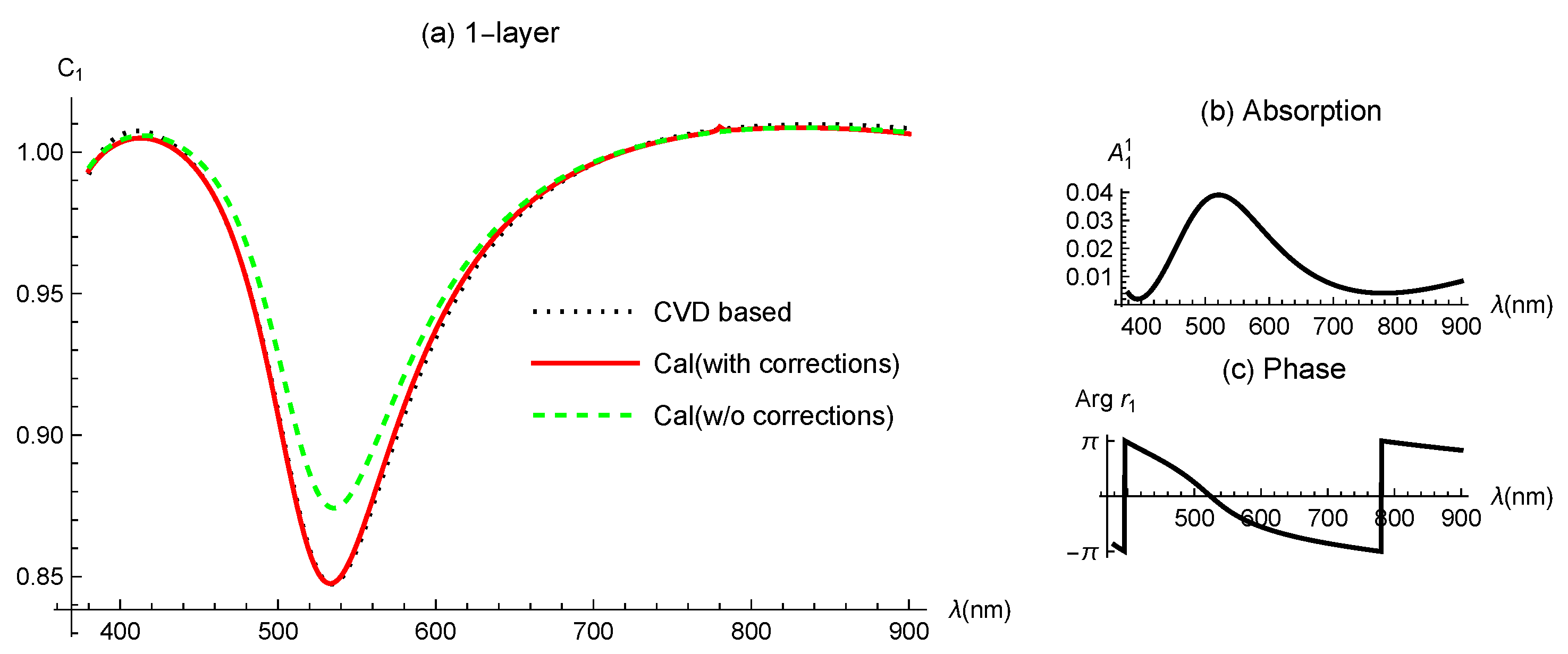
2.2. Comparison of Measured and Calculated Contrasts

Multilayer graphene was prepared by exfoliating highly oriented pyrolytic graphite (HOPG) on the same SiO2/Si substrate. The reflectance of the multilayer graphene was measured with a spectroscopic reflectometer (TohoSpec3100, Toho Technology, Nagoya, Aichi, JPN) using a × 50 objective lens. First, we determined that d SiO 2 = 268 nm from the reflectance of the substrate (Appendix A). This value is used consistently in all the calculations reported in this paper, and it results in that destructive interference occurs for R 0 at λ 520 nm. The thickness of the graphene flakes was determined by atomic force microscopy (Dimension XR, Bruker, Billerica, MA, USA).
The representative measured spectral contrasts are depicted as black dots (circles) in Figure 1 (the error bars for the data are within each circle). It is important to note that we present contrasts ( C N R N / R 0 ) instead of reflectivities ( R N ) to prevent any artificial shifts in reflectivities (see Appendix A for more details). The general feature of the spectral shapes can be elucidated as follows: for thin samples with fewer than 40 layers, the contrast is subdued due to destructive interference from the substrate, resulting in a concave structure near λ = 520 nm. For thick samples with over 60 layers, R N is predominantly influenced by contributions from the N-layer graphene and is minimally impacted by the substrate. Consequently, given that R 0 , suppressed by destructive interference, is in the denominator of the contrast, a convex structure appears near λ = 520 nm.
The contrasts, calculated using Equation (1), are represented by the red solid curves in Figure 1. A satisfactory fit with no significant deviations is achieved for various multilayer graphene samples, except for C 1 and C 3 . The observed discrepancy in these thin samples likely arises from differences in the interface between graphene and the substrate compared to that between adjacent graphene layers. This discrepancy is specific to thin samples and becomes negligible at six layers. The notable agreement between measured and calculated reflectance for visible light clearly indicates the following two facts. First, multilayer graphene can be treated as a collection of independent single layers, which is plausible since the effect of interlayer stacking does not manifest in the dynamical conductivity within the visible light range. Second, reflectance measurements provide a reliable value of layer number N, averaged within a light spot. This is true even when the thickness of the graphene flakes determined by atomic force microscopy shows positional fluctuations to a certain extent. These facts are used to validate the underlying assumption of our theoretical model of reflection presented in the subsequent sections.
C 14 and C 15 vanish at λ 2 d Si O 2 , which has been referred to as zero reflection [5,30]. Zero reflection is useful in knowing the values of basic parameters later (at the end of Section 3). To capture the essential role of graphene in achieving zero reflection, let us consider Equation (1) when cos φ = 0 . For the numerator to vanish, i ( n Si n SiO 2 2 ) cos ϕ n SiO 2 2 ε g n Si ε g sin ϕ = 0 has to be satisfied. Since ϕ is small, this equation can be simplified as i ( n Si n SiO 2 2 ) n SiO 2 2 n Si ε g d λ 2 π N = 0 , which shows that N i d SiO 2 π ε g d ( 1 n SiO 2 2 n Si ) is an approximate layer number that offers zero reflection. This argument makes it easy to understand that the dominant imaginary part of ε g is essential for zero reflection to occur.

2.3. Effective Coupling Constant

As the difference between the calculated and experimental values of contrasts proves to be sufficiently small for various multilayer graphene samples when utilizing the experimental ε g = ( n + i k ) 2 values in Equation (1), the optical constants [19] are the results that theory should ultimately elucidate. It can be inferred that nearly all the optical information of graphene multilayers is encompassed in the optical constant of monolayer graphene. This inference is partially attributed to the fact that the effect of the stacking order on the reflectance does not manifest in the visible regime. Consequently, we must inquire to what extent the theory of graphene optics can account for the n and k values.
Because of a conical energy-band structure of graphene known as the Dirac cone, the dynamical conductivity is well approximated by π α for visible light [31]. As a result, (suspended) monolayer graphene absorbs 2.3 percent ( = π α ) of the incident visible light [32]. A straightforward calculation of the Kubo formula shows that the dynamical conductivity of graphite is given by that of graphene divided by the interlayer spacing, d ( = 0.335 nm): σ graphite = π α / d [21,33,34]. The reflectance in the visible regime is free from the effects of the stacking order [35,36,37], Fermi energy position, and temperature at room temperature ranges [38]. Thus, the relative permittivity of graphite for visible light wavelengths λ is written as
ε g = ε r + i α λ 2 d ,
where ε r is the dielectric constant of the interlayer space.
By equating the right-hand side of Equation (2) with ( n + i k ) 2 , we define an effective coupling constant, α eff = 4 n k d / λ , which is compared with α in Figure 2a. The difference between α eff and α is actually larger than the order of 10 percent of α which is beyond the level of small corrections of the order of α 2 considered theoretically so far. Similarly, we define ε eff = n 2 k 2 and plot it in Figure 2b. If the interlayer space is a vacuum, an appropriate choice of ε r would be one. However, ε eff is very different from unity because the electronic wave function of the π -orbital spreads into the interlayer space, and light propagating in it is subjected to the spread of the wave function [39,40]. Fang et al. [39] calculate ε r = 6.9 using a microscopic Poisson equation which has been tested experimentally [40]. The calculated effective dielectric thickness of graphene is found to be 0.22 nm, and the microscopic dielectric permittivity decays from 6.9 in the carbon-atom plane to the vacuum permittivity within approximately 0.1 nm. Though the calculation is for the electric field pointing in the direction perpendicular to the graphene sheet, a similar (but slightly smaller) value is expected for the direction parallel to the sheet (let us assume it is 4 6 here).

3. Corrections to Reflectance by Light Emission

A substantial correction to the dynamical conductivity is deemed impermissible because, if allowed, it would result in an inconsistency with the experimental observation that a (suspended) monolayer graphene absorbs approximately 2.3 percent ( = π α ) of the incident visible light [32]. An accurate theory capable of describing reflectance does not necessitate corrections to dynamical conductivity but rather requires a mechanism that explains reflectance without altering α . The model of light emission from graphene introduced in this section serves as an illustration of such a mechanism. Our model inherently incorporates the crucial concept of wave interference, specifically coherence or incoherence, as the initial phase of light emitted from each graphene layer.

3.1. Basic Idea

Figure 3a illustrates our model of reflection, where horizontal lines on the substrate represent N-layer graphene and the vertical lines depict light rays with arrows indicating the directions of light propagation. The light rays on the left side (black in color) of Figure 3a show the primary processes of reflection (excluding contributions from light emission). In this process, incident light from a light source is transmitted and reflected by graphene, while some energy of light is absorbed by each layer. The reflection coefficient, r N , is calculated from a primary model which is defined in Section 3.2. The light rays on the right side (red in color) correspond to light emission. We suppose that the jth layer emits light. The emitted light is transmitted and reflected by graphene until the light escapes the system, and it contributes to the reflectance of the system. Thus, there is another “reflection coefficient” when N-layer graphene emits light which is defined in Section 3.3. We let z N denote the sum over such amplitudes from all layers. Once we know what r N and z N are, reflectance is given by R N = | r N + z N | 2 .
We use a transfer matrix method to calculate r N and z N [21,34]. The transfer matrix method is useful in calculating reflection (up arrow) and transmission (down) coefficients at each layer ( r N ( j ) and t N ( j ) in Figure 3a) in addition to electric field E j N ( j = 1 , , N ) that determines the absorption of the jth layer as A j N π α | E j N | 2 . The total absorption of N-layer graphene is j = 1 N A j N [21].

3.2. Primary Model

In essence, primary model means the Fresnel equation of Equation (1) where ε g is given by Equation (2). ε g has a single unknown constant ε r which can be estimated from the following observations. Ultimately, we conclude that ε r = 4.5 .
First, there must not be a large discrepancy between ε g and the experimentally determined optical constants [19,41]. Experimental values for n and k [19] are shown as • and ∘ in Figure 4a. The lines depict (bare) optical constants plotted using Equation (2) with refractive index n g = Re [ ε g ] and absorption coefficient k g = Im [ ε g ] for ε r = 4.5 and 5.5. When ε r = 4.5 , k k g , but n has a certain difference from n g . When ε r = 5.5 , n n g , but k has a certain difference from k g . Because n g increases with increasing ε r while k g decreases, there is no ε r value that can reproduce n and k simultaneously. This suggests that there should be such a discrepancy between them which is attributed to the corrections by light emission. Second, ε g has to roughly reproduce the behavior of the reflectance of multilayer graphene. It exhibits a minimum at a certain wavelength, primarily due to destructive interference caused by SiO2. As shown in Figure 4b, the position is red-shifted by increasing N, indicating that even thin graphite samples significantly impact the light interference effect. When ε r = 1 , the position changes little, and a sizable artificial shift in wavelength is needed to ensure consistency between theory and experiment, which cannot be explained as a correction. When ε r = 4.5 , a small difference between theory and experiment still remains. However, as we show later, the corrections provide better agreement not only for the wavelengths offering minimum reflectivity but also for the minimum reflectivity values, thus accounting for the difference. Third, ε r = 4.5 roughly reproduces the reflectivity of graphite in the infrared region [42]. Similar ε r values have been used to reproduce the observed reflectivities of graphite and graphene [18,19,41]. We note that the value of ε r is lesser than the magnitude of the imaginary part of ε g , since visible light has a much longer λ (400∼800 nm) than d, although α is certainly a small quantity. The optical properties of multilayer graphene are thus characterized by the large imaginary part of ε g .

3.3. Model of Light Emission

The corrections to the reflectance are the main subjects of this paper [9,10]. Specifically, we consider corrections where some fraction of the energy absorbed by the jth layer (of N-layer graphene) is transferred to light emitted from that layer (see the right side of Figure 3a). The amplitude of the emitted light is assumed to be the square root of the layer absorption, A j N π α | E j N | 2 , [34] multiplied by the branching ratio, B , i.e., B / 2 A j N , where 1 / 2 means that the light emission is direction-independent along the c-axis. We note that A j N depends not only on j and N but also on λ and d SiO 2 .
To examine how light emitted from the jth layer affects reflectance, we define two subsystems, as shown in Figure 5b: one is an isolated ( j 1 ) -layer graphene in the air; the other is ( N j ) -layer graphene on the SiO2/Si substrate. Using the transfer matrix method, we can obtain the transmission and reflection coefficients of an isolated ( j 1 ) -layer graphene in the air (denoted as t j 1 g and r j 1 g ) and the reflection coefficient of ( N j ) -layer graphene on the SiO2/Si substrate (denoted as r N j ) [21,34]. We let the reflection coefficients be X j and Y j and the transmission coefficient be Z j for the combined subsystems (see Figure 5b). These can be obtained in a self-consistent manner as follows. After calculating X j ( n ) , we add it to B / 2 A j N of the incident light to the ( j 1 ) -layer graphene (in the air) as B / 2 A j N + X j ( n ) and recalculate Y j ( n + 1 ) = r j 1 g B / 2 A j N + X j ( n ) and Z j ( n + 1 ) = t j 1 g B / 2 A j N + X j ( n ) . Then, we add a new Y j ( n + 1 ) to B / 2 A j N of the light incident to the ( N j ) -layer graphene on the SiO2/Si substrate as B / 2 A j N + Y j ( n + 1 ) and recalculate X j ( n + 1 ) = r N j B / 2 A j N + Y j ( n + 1 ) . These computations are repeated until X j and Y j converge. In this way, we can obtain analytical expressions for the converged X j , Y j , and Z j for a given B :
X j ( B ) = r N j 1 + r j 1 g 1 r N j r j 1 g B 2 A j N , Y j ( B ) = r j 1 g 1 + r N j 1 r N j r j 1 g B 2 A j N , Z j ( B ) = t j 1 g 1 + r N j 1 r N j r j 1 g B 2 A j N .
The “corrected” electric fields at an infinitesimal distance above and below the jth layer become B / 2 A j N + X j ( n ) + Y j ( n + 1 ) and B / 2 A j N + Y j ( n ) + X j ( n + 1 ) , respectively. Self-consistency, whereby lim n X j ( n ) = X j and lim n Y j ( n ) = Y j , is therefore essential to ensuring that the corrected electric field is continuous at the jth layer, which is a requirement of Maxwell’s equations. The corrected amplitude of the emitted light is written as
B 2 A j N + X j + Y j = ( 1 + r j 1 g ) 1 + r N j 1 r N j r j 1 g B 2 A j N .
By comparing this with Z j ( B ) , we see that a more accurate value of the amplitude of the emitted light is given by multiplying { } B / 2 A j N with 1 + r j 1 g as the renormalization constant, and ( 1 + r j 1 g ) { } B / 2 A j N is what b N ( j ) in Figure 3a represents. Therefore, we redefine Z j as
Z j ( B ) t j 1 g b N ( j ) ,
b N ( j ) ( 1 + r j 1 g ) 1 + r N j 1 r N j r j 1 g B 2 A j N .
We can interpret Z j ( B ) as follows. Transmission coefficient t j 1 g is the direct propagation of the renormalized light emitted from the jth layer to the air, and | t j 1 g | 2 monotonously decreases with increasing j [21]. The effects of scattering and absorption of the emitted light caused by surrounding layers is included by the part in the brace, { } . It tends to suppress the magnitude of Z j , but sometimes enhances it. For example, when N = 1 (i.e., monolayer on a substrate), the part becomes 1 + r 0 , which is larger than unity when r 0 is positive.
Figure 5. Reflectance of N-layer graphene on the SiO2/Si substrate. Dependence of the corrections to R N ( 540 nm ) (Equation (11)) on N, where d SiO 2 = 268 nm, B i n c = 0.1 , B c o h = 0.0007 and the global phase is − or +. The incoherent components are enhanced (which is called interference-enhanced Raman scattering) at around 20 layers.
Carbon 10 00018 g005
Z j ( B ) is the value at zero initial phase, so the transmission coefficient can be given a phase degree of freedom expressing the coherence or incoherence of the light emission from the different layers:
z N j = 1 N e i θ j Z j ( B ) .
Accordingly, the corrected reflectance is uniquely determined by R N r N + z N 2 = r N 2 + 2 Re r N z N * + z N 2 . The value of z N depends on these phases, θ j [43].
We consider a case in which the phase is given by a coherent phase. The exact derivation of the phase will be shown elsewhere because it is beyond the scope of the present paper. Here, we concisely explain the basic logic leading to the coherent phase in terms of quantum electrodynamics. First, we can define a quantum mechanical state of light ( | Ψ a ) that the primary model describes (see the left side of Figure 3). All the information of light is expressed by coefficients r N ( j ) and t N ( j ) ( j = 1 , , N ). Second, we can also define another quantum state of light ( | Ψ b ) for the emitted light (see the right side of Figure 3). All the information of emitted light is expressed by coefficients b N ( j ) . These two states have an overlap, b N * ( j ) t N ( j ) + b N * ( j ) r N ( j ) , caused by jth-layer graphene. Thus, if we consider a linear superposition of these states as | Ψ a + e i θ | Ψ b to form energy eigenstates, phase e i θ j must be chosen so that e i θ j b N * ( j ) ( t N ( j ) + r N ( j ) ) becomes a real number, namely
e i θ j = ± t N ( j ) + r N ( j ) | t N ( j ) + r N ( j ) | b N ( j ) * | b N ( j ) | .
Factor ± is a global phase ( θ ) in the sense that it is independent of the value of j. Because the scattered light ( r N ) and the emitted light ( z N ) form a two-level state, there are two possible linear superpositions of their energy eigenstates, 1 ( θ = π ) or + 1 ( θ = 0 ). The minus sign ( e i π ) is assigned to the lower energy state. From Equations (5) and (8), we obtain e i θ j Z j ( B ) = ± t N ( j ) + r N ( j ) | t N ( j ) + r N ( j ) | t j 1 g | b N ( j ) | .
Including the correction due to coherent light emission leads to
R N = r N + j = 1 N e i θ j Z j ( B c o h ) 2 ,
where B c o h is the branching ratio of the energy of the emitted coherent photons to that of the absorbed photons. Since coherent photon emission is related to the electron–photon coupling strength of the annihilated photo-excited electron–hole pairs, B c o h should be on the order of ( π α ) 2 and insensitive to changes in N.
Next, we apply R N = r N 2 + 2 Re r N z N * + z N 2 to the case of θ j in z N being a random variable. Here, the definition of randomness is that if we take the time average regarding θ j , we have Re r N z N * = 0 and z N 2 = j = 1 N | Z j ( B ) | 2 . We refer to this case as incoherent corrections, which also include the cases that the global phase takes 0 and π if there is a perturbation that can mix the two energy levels. An interference term is now included in z N 2 as the last term of
z N 2 = i = 1 N | Z i ( B ) | 2 + i j e i ( θ i θ j ) Z i ( B ) Z j * ( B ) ,
but it vanishes when taking the time average and only the first term of the incoherent corrections remains [44]. Inelastic scattering of light such as Raman scattering is usually considered to give rise to incoherent photons. We let B i n c be the branching ratio of the energy of the emitted incoherent photons to that of absorbed photons. Since Z j ( B i n c ) is proportional to B i n c A j N (Equation (3)), the incoherent corrections are proportional to B i n c A j N . For Raman scattering, parameter B i n c is fundamentally determined by the electron–photon and electron–phonon coupling strengths, and it should not be so sensitive to the change in N. Indeed, the incoherent corrections with constant B i n c follow the measured N dependence of the G band Raman intensity (Section 4.3). The G band consists of optical phonons at the Γ point, whose lattice vibrations are in-plane.
A generalized reflection formula covering the above two cases (coherent and incoherent corrections) can be written as
R N ( λ , θ , B c o h , B i n c ) r N + e i θ j = 1 N t N ( j ) + r N ( j ) | t N ( j ) + r N ( j ) | b N ( j ) * | b N ( j ) | Z j ( B c o h ) 2 + j = 1 N | Z j ( B i n c ) | 2
when B c o h = B i n c = 0 , R N ( λ , θ , B c o h , B i n c ) reduces to Equation (1) with Equation (2). Figure 5 shows the N dependence of R N ( λ , θ , 0 , 0 ) (dashed), R N ( λ , π , B c o h = 0.0007 , 0 ) (red), R N ( λ , 0 , B c o h = 0.0007 , 0 ) (blue), and j = 1 N | Z j ( B i n c = 0.1 ) | 2 (black) for a fixed λ = 540 nm. We note that the incoherent corrections always increase the reflectance and preclude zero reflections at N 15 , which is in contrast to the coherent corrections. Moreover, the G band Raman intensity is enhanced when zero reflection occurs [10,45,46,47]. This situation is called interference-enhanced Raman scattering, [9], and it is reasonably reproduced in Equation (11). The experimental fact that zero reflection is observed at N 15 (see 14 and 15 layers in Figure 1) shows that B c o h 0.0007 , B i n c is much smaller than 0.1, and θ = π (red curve in Figure 5).

4. Applications of Model

In this section, we show that the discrepancy between the measured reflectance of multilayer graphene (Figure 1) and the prediction of the model (Equation (11)) is sufficiently small for the present purpose. Our model is therefore nearly equivalent to the Fresnel equation with the experimental optical constants (n and k) [19] while our model can describe the interesting aspects of reflection. Using monolayer graphene, we provide a detailed explanation of the mechanism modifying reflectance without introducing any artificial change in dynamical conductivity. To showcase the versatility of our model, we also explore Raman scattering as incoherent corrections.

4.1. Comparison of Theory and Experiment

Calculated contrasts are shown in Figure 6 as red solid curves, which include coherent corrections only (i.e., B i n c = 0 ). Green dashed curves represent the primary model of Equation (1), which does not include any corrections due to light emission. All calculations were performed with B c o h = 0.0007 , where this value was chosen so that we could obtain good agreement between the calculations and observations for all layers. We note that this value is consistent with zero reflection being observed for N 15 .
From the consistency between the calculated and measured contrasts shown in Figure 6 (except C 1 and C 3 ), we can draw two main conclusions. First, the π phase ( θ = π ) of the coherent corrections is essential. If we adopt the zero phase ( θ = 0 ), a serious discrepancy arises, as can be readily imagined from the relative location of the red solid curves with respect to the green dashed ones. Second, the incoherent corrections are rather small. In fact, for most of the layers examined (not shown in Figure 6), the incoherent corrections did not improve the fitting. Our estimated reasonable range of B i n c is less than 0.01.
Only for the 226-layer variant is there a slight but non-negligible deviation of the red solid curve from the measured contrast. A relatively small difference between the red solid and green dashed curves shows that the strength of | r N + z N | 2 | r N | 2 is suppressed and that z N is under some special phase balance by interference for N 226 . Thus, a slight shift in θ j might improve the fitting. For example, second-order corrections which arise due to a self-consistent calculation of E j N (and A j N ) might be relevant to this.

4.2. Monolayer

Unfortunately, the Fresnel equation is inconsistent with the measured contrast of monolayer graphene (see C 1 in Figure 1), probably because reflectance depends on the condition of the interface between graphene and substrates. However, as we carefully confirmed that almost all the information of the corrections from the emitted light is included in the reflectance of monolayer graphene, we believe that contrast C 1 calculated from the Fresnel equation with experimental n and k values is the result that we should compare with the model.
In Figure 7a, we present simulated (black dotted) and calculated (green dashed and red solid) spectral contrasts of monolayer graphene on the SiO2/Si substrate. Clearly, the corrections are of physical significance; black dots and red solid curve almost perfectly match. In R 1 = | r 1 + z 1 | 2 , r 1 becomes a positive number only near λ = 2 d SiO 2 as shown in Figure 7c. This is due to the destructive interference caused by SiO2, which also increases absorption because A 1 1 = π α | 1 + r 1 | 2 . This enhanced absorption leads to the main difference between the reflectances from the substrate ( R 0 ) and from the graphene on it ( R 1 ), increasing the visibility of graphene. Correction due to light emission z 1 is a negative number due to the negative global phase of an energetically stable configuration of light. Thus, the corrections increase | R 1 R 0 | . Namely, the increase in the visibility of graphene is mainly due to the substrate-induced enhancement of light absorption and is partly due to light emission.
It is important to note that the primary model can explain the measured contrasts if α is more than 20 percent larger than 1 / 137 . However, this immediately leads to an inconsistency with the experimental fact that (suspended) monolayer graphene absorbs 2.3 percent ( = π α ) of the incident visible light [32]. Additionally, the primary model with such corrections to α does not reproduce the measured contrasts of many samples with different thickness. Furthermore, the primary model is not applicable to the Raman effect, while our model can include it in a natural way, as shown below.

4.3. Raman Scattering as Incoherent Corrections

We measured the G band Raman peak intensity as a function of layer number in order to verify the interpretation of Raman scattering being an incoherent light emission [10]. The incoherent correction is defined by the last term of Equation (11) as I N j = 1 N | Z j ( B i n c ) | 2 . I N is proportional to B i n c and does not depend on the value of B i n c when scaled. As shown in Figure 8, there is a reasonable similarity between the measured Raman intensity (dots) and calculated incoherent component (dashed curve). Also plotted is an approximation of I N (dot-dashed curve) defined by
I N direct B i n c 2 j = 1 N | t j 1 g | 2 A j N
to show the effect of multiple scattering of incoherent light. The approximation overestimates the intensity for thick samples, as readily imagined.
On the other hand, there is a noticeable discrepancy between them for samples with fewer than 30 layers, where there is a dip in the reflectance that is similar to the observation by No et al. [47]. The assumption of a random phase for θ j in Equation (7) is a possible reason for the discrepancy, because random phases can undergo synchronization or entrainment [43]. An intermediate state of phase θ j that is neither random nor perfectly coherent may account for the behavior.

5. Discussion

There is a possibility that substrates play a decisive role in determining the selection of the two states specified by global phase θ (0 and π ). To see this, let us consider monolayer graphene suspended in the air. From Equation (1), the reflection and transmission coefficients (without substrates) are r 1 π α / 2 and t 1 1 π α / 2 , and the absorption is given by A 1 1 = 1 r 1 2 t 1 2 π α . Light emission modifies the reflection coefficient as follows:
r 1 + e i θ Z 1 ( B ) = π α 2 + e i θ B 2 π α .
The magnitude of the second term is 0.0028 when B = 0.0007 , which is about 25 percent the magnitude of the first term (0.011). The reflection increases or decreases depending on θ . When θ = π (0), the correction term is negative (positive) in sign; therefore, the light emission increases (decreases) the reflectance. Mathematically speaking, the change in the reflectance is equivalent to a replacement of α as α α eff = α e i θ π B / 2 α . This immediately leads to an inconsistency with the experimental fact that suspended monolayer graphene absorbs 2.3 percent ( = π α , the measured uncertainty is within 5 percent of π α ) of the incident visible light [32]. This inconsistency is resolved by considering that for graphene suspended in the air, the states of θ = π and 0 are degenerate, and the effect of light emission effectively disappears by interference. This contrasts with monolayer graphene on SiO2/Si substrates for which θ = π is selected.
Since coherent and incoherent emissions are two extreme cases (uniform and random) of phase θ j in Equation (7), a sharp distinction between the coherent and incoherent emissions is not always possible. The proper way to calculate the reflectance is to derive a dynamical model of θ j at a microscopic level [43,48] and use it to calculate R N = r N + j = 1 N e i θ j Z j ( B ) 2 . Especially in the case of monolayer, they are inseparable as
R 1 = r 1 + e i θ 1 Z 1 ( B c o h ) + e i ϕ 1 Z 1 ( B i n c ) 2 ,
when ϕ 1 and θ 1 have some correlation. Then, the reflectance is always subject to fluctuations created by the last term (through electron–phonon interactions).
Our model postulates that the effect of the emitted light appears as a correction to the reflection (and transmission) coefficient, not as a correction to dynamical conductivity. Meanwhile, spontaneous emission is generally treated as a loss, and it is often included as a phenomenological relaxation constant in dynamical conductivity. For example, in Ref. [19], the authors introduce relaxation constants for the Drude–Lorentz oscillator model to interpret the measured optical constants. However, an excessively large relaxation constant (or very short lifetime) for the Drude term (0.6 fs) already raises concerns about the naturalness of including such a relaxation parameter [49]. The justification of our postulate needs a theoretical clarification at a more fundamental level of quantum electrodynamics, which is capable of describing photon creation and annihilation, while the excellent agreement between the model and experiments clearly shows that this postulate works well. Our model is also consistent with a theoretical result that dynamical conductivity is free from such a correction when graphene is undoped (i.e., the charge neutrality condition is satisfied) [31]. Moreover, the model explains the N-dependence of Raman intensity as incoherent corrections (Section 4.3), besides the contrast, in a unified manner.

6. Conclusions

In summary, we succeeded in explaining the measured visible contrasts of multilayer graphene samples on a SiO2/Si substrate by including coherent light emissions that come from some fraction ( B c o h = 0.0007 ) of the absorbed photon energy. Coherent corrections are essential for assuring the consistency between theory and experiment, while incoherent corrections can be neglected for contrast.
Photo-excited electrons contribute insignificantly to light emission when they are distant from the bottom of the conduction band. Namely, the value of B for those electrons is suppressed. In fact, graphene lacks a bandgap, and the branching ratio of coherent light emission to absorbed light is very small ( B c o h = 0.0007 ). What we argued for in this paper is corrections (to the main effect) that have small branching ratios. However, whether light emission from those electrons can be entirely neglected depends on various factors. Graphene serves as an interesting example where corrections are greatly enhanced by its large absorption. The destructive interference effect from the substrate and the multilayer-induced coherence are the means by which it is observable in the reflectance. Similar emission-based corrections could be anticipated for other layered materials without band gaps, and the method developed here may prove useful in accurately understanding their optical properties.
Our formulation of the reflectance using the transfer matrix method has a descriptive ability for layered materials having defects and irregularities. For this reason, and considering the success it has had in describing the reflectance of relatively simple systems (graphene multilayer at visible range), we believe that some future form of this theory may be useful in describing the optical properties of any layered material with or without a band gap.

Author Contributions

Conceptualization, K.-i.S. and T.M.; sample preparation and measurment, M.K., T.Y., T.O. and T.M.; analysis, K.-i.S., K.H. and M.K.; writing—original draft preparation, K.-i.S.; writing—review and editing, K.-i.S.; project administration, K.-i.S. and T.M.; funding acquisition, T.M. All authors have read and agreed to the published version of the manuscript.

Funding

This research received no external funding.

Data Availability Statement

The data presented in this study are available on reasonable request from the corresponding author.

Acknowledgments

K.-i.S. thanks Y. Sekine, H. Endo, and Y. Taniyasu for raising helpful questions on this subject. A part of this work was supported by “Nanotechnology Platform Japan” of the Ministry of Education, Culture, Sports, Science and Technology (MEXT), Grant Number JPMXP09F21UT0045, and the reflectance measurement was conducted in the Takeda Cleanroom with the help of the Nanofabrication Platform Center of the School of Engineering, University of Tokyo, Japan.

Conflicts of Interest

Ken-ichi Sasaki and Kenichi Hitachi were employed by the company NTT Corporation; Masahiro Kamada, Takamoto Yokosawa, Taisuke Ochi and Tomohiro Matsui were employed by the company Anritsu Corporation. The authors declare that the research was conducted in the absence of any commercial or financial relationships that could be construed as a potential conflict of interest.

Appendix A. Measured Reflectivities

We performed reflectivity measurements three times on the same sample (Run 1, Run 2, and Run 3). All measurements were consistent in the sense that the measured reflectivities of N-layer graphene on the substrate ( R N ) divided by that of the SiO2/Si substrate ( R 0 ), that is, the contrast ( C N = R N / R 0 ), were identical. Therefore, we compared C N with calculations in the main text. However, while R 0 values of Run 2 and Run 3 were identical, the R 0 of Run 1 deviated from that of Run 2 (Run 3), as shown in Figure A1. The same contrast also means that the values of R N for Run 2 and Run 3 were identical, while the R N for Run 1 deviated from that of Run 2 (Run 3). The discrepancy between the R 0 of Run 1 and that of Run 2 (Run 3) was presumably brought about by a change in the focal point along the depth direction when a reference substrate was replaced with the target sample. This could change the incident light intensity and lead to a discrepancy in R N between Run 1 and Run 2 (Run 3).
A problem arises when we determine the value of d Si O 2 from R 0 . Considering that the wavelength producing the reflectivity minimum is the same for the three runs, we can determine d Si O 2 = 268 nm by assuming that n Si O 2 is the standard value (≃1.46) [29]. These parameters reasonably reproduce R 0 of Run 2 (Run 3) (Figure A1). Meanwhile, 268 nm is inconsistent with another estimation using a reflectometer ( 274 ± 1 nm), which results in n Si O 2 1.43 to reproduce the wavelength producing the reflectivity minimum by destructive interference (the same n Si O 2 d Si O 2 ). When we choose n Si O 2 1.43 for d Si O 2 = 274 nm, the corresponding R 0 is the (blue) dashed curve, which reproduces R 0 of Run 1 around the reflectivity minimum (the two curves overlap from 460 to 560 nm) and approaches R 0 of Run 2 (Run 3) away from the reflectivity minimum ( λ < 460 nm and λ > 560 nm). Since n Si O 2 1.43 is an acceptable value, we need to be mindful of the possibility that a true R 0 is neither the R 0 of Run 1 nor that of Run 2 (run 3). Because we assumed that the refractive index of Si is the commonly used value, we kept the same standpoint for SiO2. Ultimately, we concluded that d Si O 2 = 268 nm.
Figure A1. Determination of SiO2 thickness. Measured (black (Run) and gray (Run 2 (Run 3)) dots) and calculated (green and blue dashed curves) spectral reflectivities of N-layer graphene on the same SiO2/Si substrate. A white-light source was used, and reflectivity was measured at room temperature. The horizontal axis is λ (nm), and the reliable range of our spectrometer is 450 to 800 nm.
Carbon 10 00018 g0a1

References

  1. Novoselov, K.S.; Geim, A.K.; Morozov, S.V.; Jiang, D.; Katsnelson, M.I.; Grigorieva, I.V.; Dubonos, S.V.; Firsov, A.A. Two-dimensional gas of massless Dirac fermions in graphene. Nature 2005, 438, 197–200. [Google Scholar] [CrossRef]
  2. Zhang, Y.; Tan, Y.W.; Stormer, H.L.; Kim, P. Experimental observation of the quantum Hall effect and Berry’s phase in graphene. Nature 2005, 438, 201–204. [Google Scholar] [CrossRef]
  3. Novoselov, K.S.; Jiang, D.; Schedin, F.; Booth, T.J.; Khotkevich, V.V.; Morozov, S.V.; Geim, A.K. Two-dimensional atomic crystals. Proc. Natl. Acad. Sci. USA 2005, 102, 10451–10453. [Google Scholar] [CrossRef]
  4. Blake, P.; Hill, E.W.; Neto, A.H.C.; Novoselov, K.S.; Jiang, D.; Yang, R.; Booth, T.J.; Geim, A.K. Making graphene visible. Appl. Phys. Lett. 2007, 91, 063124. [Google Scholar] [CrossRef]
  5. Roddaro, S.; Pingue, P.; Piazza, V.; Pellegrini, V.; Beltram, F. The optical visibility of graphene: Interference colors of ultrathin graphite on SiO2. Nano Lett. 2007, 7, 2707–2710. [Google Scholar] [CrossRef]
  6. Ni, Z.H.; Wang, H.M.; Kasim, J.; Fan, H.M.; Yu, T.; Wu, Y.H.; Feng, Y.P.; Shen, Z.X. Graphene Thickness Determination Using Reflection and Contrast Spectroscopy. Nano Lett. 2007, 7, 2758–2763. [Google Scholar] [CrossRef] [PubMed]
  7. Casiraghi, C.; Hartschuh, A.; Lidorikis, E.; Qian, H.; Harutyunyan, H.; Gokus, T.; Novoselov, K.S.; Ferrari, A.C. Rayleigh Imaging of Graphene and Graphene Layers. Nano Lett. 2007, 7, 2711–2717. [Google Scholar] [CrossRef]
  8. Ghamsari, B.G.; Tosado, J.; Yamamoto, M.; Fuhrer, M.S.; Anlage, S.M. Measuring the Complex Optical Conductivity of Graphene by Fabry-Pérot Reflectance Spectroscopy. Sci. Rep. 2016, 6, 34166. [Google Scholar] [CrossRef]
  9. Nemanich, R.J.; Tsai, C.C.; Connell, G.A.N. Interference-Enhanced Raman Scattering of Very Thin Titanium and Titanium Oxide Films. Phys. Rev. Lett. 1980, 44, 273–276. [Google Scholar] [CrossRef]
  10. Wang, Y.Y.; Ni, Z.H.; Shen, Z.X.; Wang, H.M.; Wu, Y.H. Interference enhancement of Raman signal of graphene. Appl. Phys. Lett. 2008, 92, 043121. [Google Scholar] [CrossRef]
  11. Stöhr, R.J.; Kolesov, R.; Pflaum, J.; Wrachtrup, J. Fluorescence of laser-created electron-hole plasma in graphene. Phys. Rev. B 2010, 82, 121408. [Google Scholar] [CrossRef]
  12. Lui, C.H.; Mak, K.F.; Shan, J.; Heinz, T.F. Ultrafast photoluminescence from graphene. Phys. Rev. Lett. 2010, 105, 127404. [Google Scholar] [CrossRef]
  13. Liu, W.T.; Wu, S.W.; Schuck, P.J.; Salmeron, M.; Shen, Y.R.; Wang, F. Nonlinear broadband photoluminescence of graphene induced by femtosecond laser irradiation. Phys. Rev. B 2010, 82, 081408. [Google Scholar] [CrossRef]
  14. Suemoto, T.; Sakaki, S.; Nakajima, M.; Ishida, Y.; Shin, S. Access to hole dynamics in graphite by femtosecond luminescence and photoemission spectroscopy. Phys. Rev. B Condens. Matter Mater. Phys. 2013, 87, 224302. [Google Scholar] [CrossRef]
  15. Riaz, A.; Pyatkov, F.; Alam, A.; Dehm, S.; Felten, A.; Chakravadhanula, V.S.; Flavel, B.S.; Kübel, C.; Lemmer, U.; Krupke, R. Light emission, light detection and strain sensing with nanocrystalline graphene. Nanotechnology 2015, 26, 325202. [Google Scholar] [CrossRef]
  16. Song, J.C.; Tielrooij, K.J.; Koppens, F.H.; Levitov, L.S. Photoexcited carrier dynamics and impact-excitation cascade in graphene. Phys. Rev. B Condens. Matter Mater. Phys. 2013, 87, 155429. [Google Scholar] [CrossRef]
  17. Massicotte, M.; Soavi, G.; Principi, A.; Tielrooij, K.J. Hot carriers in graphene-fundamentals and applications. Nanoscale 2021, 13, 8376–8411. [Google Scholar] [CrossRef]
  18. Castriota, M.; Politano, G.G.; Vena, C.; De Santo, M.P.; Desiderio, G.; Davoli, M.; Cazzanelli, E.; Versace, C. Variable Angle Spectroscopic Ellipsometry investigation of CVD-grown monolayer graphene. Appl. Surf. Sci. 2019, 467–468, 213–220. [Google Scholar] [CrossRef]
  19. El-Sayed, M.A.; Ermolaev, G.A.; Voronin, K.V.; Romanov, R.I.; Tselikov, G.I.; Yakubovsky, D.I.; Doroshina, N.V.; Nemtsov, A.B.; Solovey, V.R.; Voronov, A.A.; et al. Optical Constants of Chemical Vapor Deposited Graphene for Photonic Applications. Nanomaterials 2021, 11, 1230. [Google Scholar] [CrossRef]
  20. Devang, P.; Simone, D.; Naga, A.P.; Kumar, S.; Ralph, K. Enhanced Broadband Photodetection with Geometry and Interface Engineered Nanocrystalline Graphite. Adv. Sensor Res. 2023, 2023, 2300134. [Google Scholar] [CrossRef]
  21. Sasaki, K.; Hitachi, K. Universal layer number in graphite. Commun. Phys. 2020, 3, 90. [Google Scholar] [CrossRef]
  22. Hendry, E.; Hale, P.J.; Moger, J.; Savchenko, A.K.; Mikhailov, S.A. Coherent nonlinear optical response of graphene. Phys. Rev. Lett. 2010, 105, 097401. [Google Scholar] [CrossRef]
  23. Sun, Z.; Hasan, T.; Torrisi, F.; Popa, D.; Privitera, G.; Wang, F.; Bonaccorso, F.; Basko, D.M.; Ferrari, A.C. Graphene mode-locked ultrafast laser. ACS Nano 2010, 4, 803–810. [Google Scholar] [CrossRef] [PubMed]
  24. Mikhailov, S.A. Theory of the nonlinear optical frequency mixing effect in graphene. Phys. E Low Dimens. Syst. Nanostruct. 2012, 44, 924–927. [Google Scholar] [CrossRef]
  25. Yang, H.; Guan, H.; Biekert, N.; Arefe, G.; Chang, D.C.; Sun, Y.; Yeh, P.C.; Liu, X.; Hong, S.Y.; Marion, I.D.; et al. Layer dependence of third-harmonic generation in thick multilayer graphene. Phys. Rev. Mater. 2018, 2, 071002. [Google Scholar] [CrossRef]
  26. Stauber, T.; Peres, N.M.R.; Geim, A.K. Optical conductivity of graphene in the visible region of the spectrum. Phys. Rev. B 2008, 78, 085432. [Google Scholar] [CrossRef]
  27. Stauber, T.; Parida, P.; Trushin, M.; Ulybyshev, M.V.; Boyda, D.L.; Schliemann, J. Interacting Electrons in Graphene: Fermi Velocity Renormalization and Optical Response. Phys. Rev. Lett. 2017, 118, 266801. [Google Scholar] [CrossRef]
  28. Aspnes, D.E.; Studna, A.A. Dielectric functions and optical parameters of Si, Ge, GaP, GaAs, GaSb, InP, InAs, and InSb from 1.5 to 6.0 eV. Phys. Rev. B 1983, 27, 985. [Google Scholar] [CrossRef]
  29. Malitson, I.H. Interspecimen Comparison of the Refractive Index of Fused Silica. J. Opt. Soc. Am. 1965, 55, 1205–1209. [Google Scholar] [CrossRef]
  30. Anders, H. Thin Films in Optics; The Focal Press: Waltham, MA, USA, 1965. [Google Scholar]
  31. Ando, T.; Zheng, Y.; Suzuura, H. Dynamical Conductivity and Zero-Mode Anomaly in Honeycomb Lattices. J. Phys. Soc. Jpn. 2002, 71, 1318–1324. [Google Scholar] [CrossRef]
  32. Nair, R.R.; Blake, P.; Grigorenko, A.N.; Novoselov, K.S.; Booth, T.J.; Stauber, T.; Peres, N.M.R.; Geim, A.K. Fine Structure Constant Defines Visual Transparency of Graphene. Science 2008, 320, 1308. [Google Scholar] [CrossRef]
  33. Kuzmenko, A.B.; van Heumen, E.; Carbone, F.; van der Marel, D. Universal Optical Conductance of Graphite. Phys. Rev. Lett. 2008, 100, 117401. [Google Scholar] [CrossRef]
  34. Sasaki, K.i. Layered Dynamical Conductivity for a Transfer Matrix Method —Application to an N-layer Graphene—. J. Phys. Soc. Jpn. 2020, 89, 094706. [Google Scholar] [CrossRef]
  35. Taft, E.A.; Philipp, H.R. Optical Properties of Graphite. Phys. Rev. 1965, 138, A197–A202. [Google Scholar] [CrossRef]
  36. Ichikawa, Y.H.; Kobayashi, K. Optical properties of graphite in the infrared region. Carbon 1966, 3, 401–406. [Google Scholar] [CrossRef]
  37. Dresselhaus, M.S.; Dresselhaus, G. Interpretation of infrared modulation spectroscopy data in graphite by the Slonczewski-Weiss- McClure band model. Phys. Rev. B 1976, 13, 4635–4636. [Google Scholar] [CrossRef]
  38. Klimchitskaya, G.L.; Mostepanenko, V.M.; Petrov, V.M. Impact of chemical potential on the reflectance of graphene in the infrared and microwave domains. Phys. Rev. A 2018, 98, 023809. [Google Scholar] [CrossRef]
  39. Fang, J.; Vandenberghe, W.G.; Fischetti, M.V. Microscopic dielectric permittivities of graphene nanoribbons and graphene. Phys. Rev. B 2016, 94, 045318. [Google Scholar] [CrossRef]
  40. Rickhaus, P.; Liu, M.H.; Kurpas, M.; Kurzmann, A.; Lee, Y.; Overweg, H.; Eich, M.; Pisoni, R.; Taniguchi, T.; Watanabe, K.; et al. The electronic thickness of graphene. Sci. Adv. 2020, 6, eaay8409. [Google Scholar] [CrossRef]
  41. Bruna, M.; Borini, S. Optical constants of graphene layers in the visible range. Appl. Phys. Lett. 2009, 94, 031901. [Google Scholar] [CrossRef]
  42. Djurišić, A.B.; Li, E.H. Optical properties of graphite. J. Appl. Phys. 1999, 85, 7404–7410. [Google Scholar] [CrossRef]
  43. Kuramoto, Y. Chemical Oscillations, Waves, and Turbulence; Springer: Berlin/Heidelberg, Germany, 1984. [Google Scholar] [CrossRef]
  44. Velson, N.V.; Velson, N.V.; Zobeiri, H.; Wang, X.; Wang, X. Rigorous prediction of Raman intensity from multi-layer films. Opt. Express 2020, 28, 35272–35283. [Google Scholar] [CrossRef]
  45. Yoon, D.; Moon, H.; Cheong, H.; Choi, J.S.; Choi, J.A.; Park, B.H. Variations in the Raman Spectrum as a Function of the Number of Graphene Layers. J. Korean Phys. Soc. 2009, 55, 1299–1303. [Google Scholar] [CrossRef]
  46. Li, X.L.; Qiao, X.F.; Han, W.P.; Lu, Y.; Tan, Q.H.; Liu, X.L.; Tan, P.H. Layer number identification of intrinsic and defective multilayered graphenes up to 100 layers by the Raman mode intensity from substrates. Nanoscale 2015, 7, 8135–8141. [Google Scholar] [CrossRef]
  47. No, Y.S.; Choi, H.K.; Kim, J.S.; Kim, H.; Yu, Y.J.; Choi, C.G.; Choi, J.S. Layer number identification of CVD-grown multilayer graphene using Si peak analysis. Sci. Rep. 2018, 8, 571. [Google Scholar] [CrossRef]
  48. Dicke, R.H. Coherence in Spontaneous Radiation Processes. Phys. Rev. 1954, 93, 99. [Google Scholar] [CrossRef]
  49. Toqeer, I.; Yaqoob, M.Z.; Ghaffar, A.; Alkanhal, M.A.S.; Khan, Y.; Aladadi, Y.T. Reflectance and transmittance of terahertz waves from graphene embedded into metamaterial structures. J. Opt. Soc. Am. A 2021, 38, 465–475. [Google Scholar] [CrossRef]
Figure 1. Measured (black circles) and calculated (red solid) spectral contrasts of N-layer graphene on the same SiO2/Si substrate. The measurments were conducted using a white-light source at room temperature. The red solid curves were obtained from Equation (1) with ε g = ( n + i k ) 2 using optical constants obtained by El-Sayed et al. [19]. The horizontal axis is λ (nm), and the reliable range of our spectrometer is 450 to 800 nm.
Carbon 10 00018 g001
Figure 2. Effective coupling constants. (a) Plot of α eff calculated with the optical constants obtained by El-Sayed et al. [19]. The horizontal axis is λ (nm). (b) Plot of ε eff .
Carbon 10 00018 g002
Figure 3. Model description. (a) The primary (left side) and secondary (right side) processes involved in the reflection are physically interconnected through light absorption at each graphene layer. (b) The self-consistent calculation of Z j is explained in detail in the text.
Carbon 10 00018 g003
Figure 4. ε r of the primary model. (a) Experimental n and k values are represented by dots, taken from Ref. [19]. The lines depict bare optical constants without corrections. (b) Dots indicate measured wavelengths corresponding to the minimum reflectance. A comparison between the measured and calculated results suggests that ε r = 4.5 is a reasonable value.
Carbon 10 00018 g004
Figure 6. Measured (black circles) and calculated (green dashed and red solid) spectral contrasts of N-layer graphene on the same SiO2/Si substrate. The green dashed curves represent the primary model (Equation (1) with Equation (2)) which does not include corrections. The red solid curves include coherent corrections. The horizontal axis is λ (nm), and the reliable range of our spectrometer is 450 to 800 nm.
Carbon 10 00018 g006
Figure 7. Contrasts of monolayer graphene on SiO2/Si substrates. (a) One contrast is calculated using Equation (1) with experimental ε g (black dotted), while the other two curves are obtained using the model with corrections (red solid curve) and without corrections (green dashed curve). The increased visibility of graphene is primarily attributed to substrate-induced enhancement of light absorption and partly to light emission. (b) Layer absorption of monolayer graphene on SiO2/Si substrates A 1 1 = π α | 1 + r 1 | 2 . The destructive interference effect of the substrate enhances absorption near λ 2 d SiO 2 , where r 1 is a positive number (c).
Carbon 10 00018 g007
Figure 8. Raman intensity as incoherent corrections. The dots represent the measured peak intensity of the Raman G band when using a light source with a wavelength of 532 nm. The dashed curve corresponds to the incoherent correction, while the dot-dashed curve is an approximation that ignores multiple scattering.
Carbon 10 00018 g008
Disclaimer/Publisher’s Note: The statements, opinions and data contained in all publications are solely those of the individual author(s) and contributor(s) and not of MDPI and/or the editor(s). MDPI and/or the editor(s) disclaim responsibility for any injury to people or property resulting from any ideas, methods, instructions or products referred to in the content.

