
Spin-Filter Magnetic Tunnel Junctions Based on A-Type Antiferromagnetic CrSBr with Giant Tunnel Magnetoresistance

Abstract
:1. Introduction
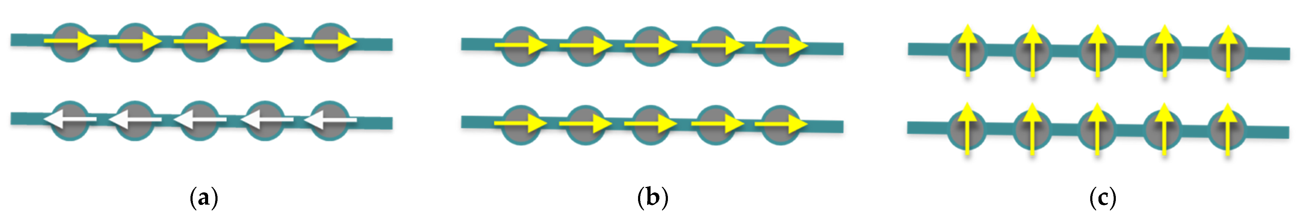
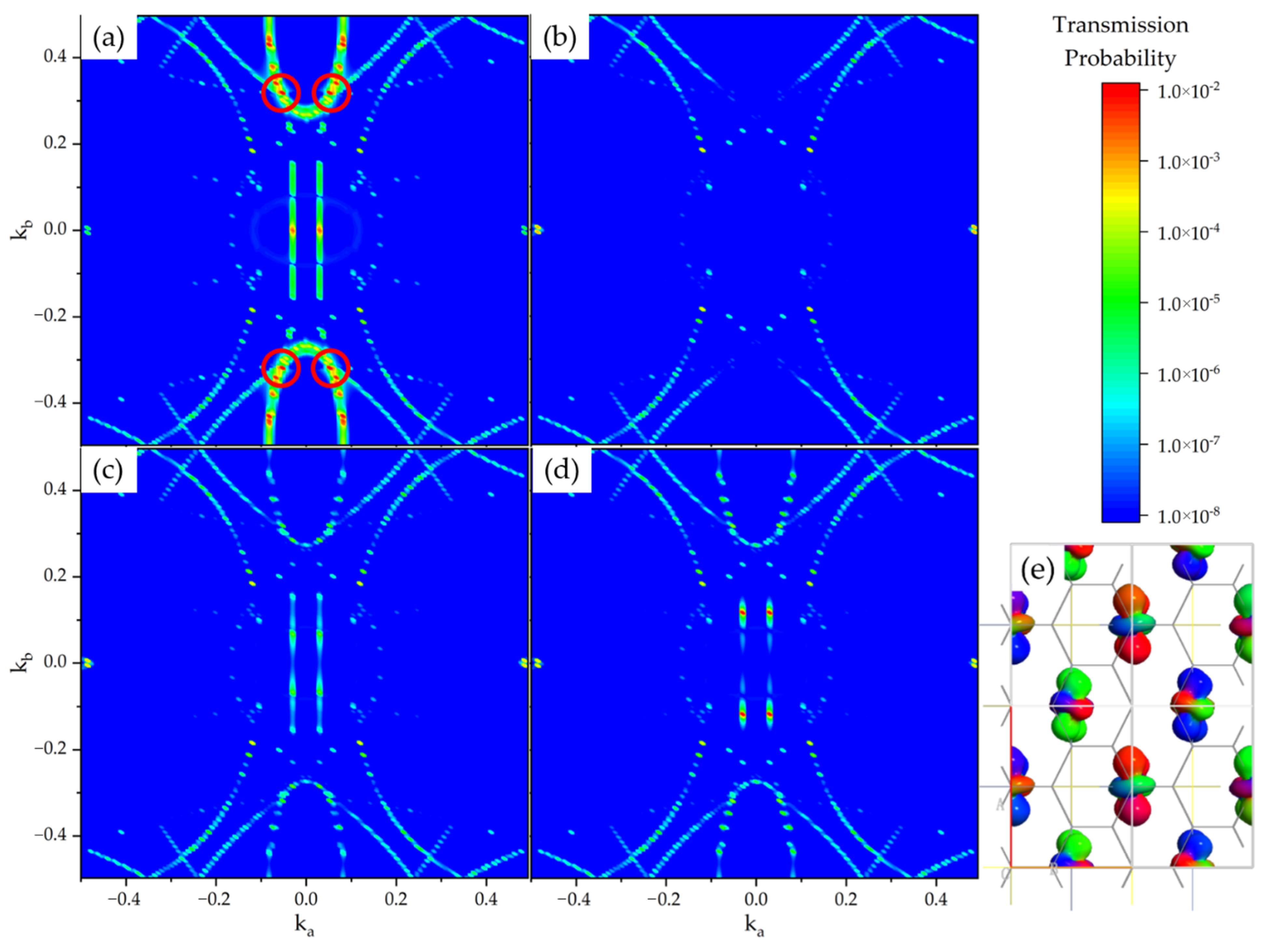
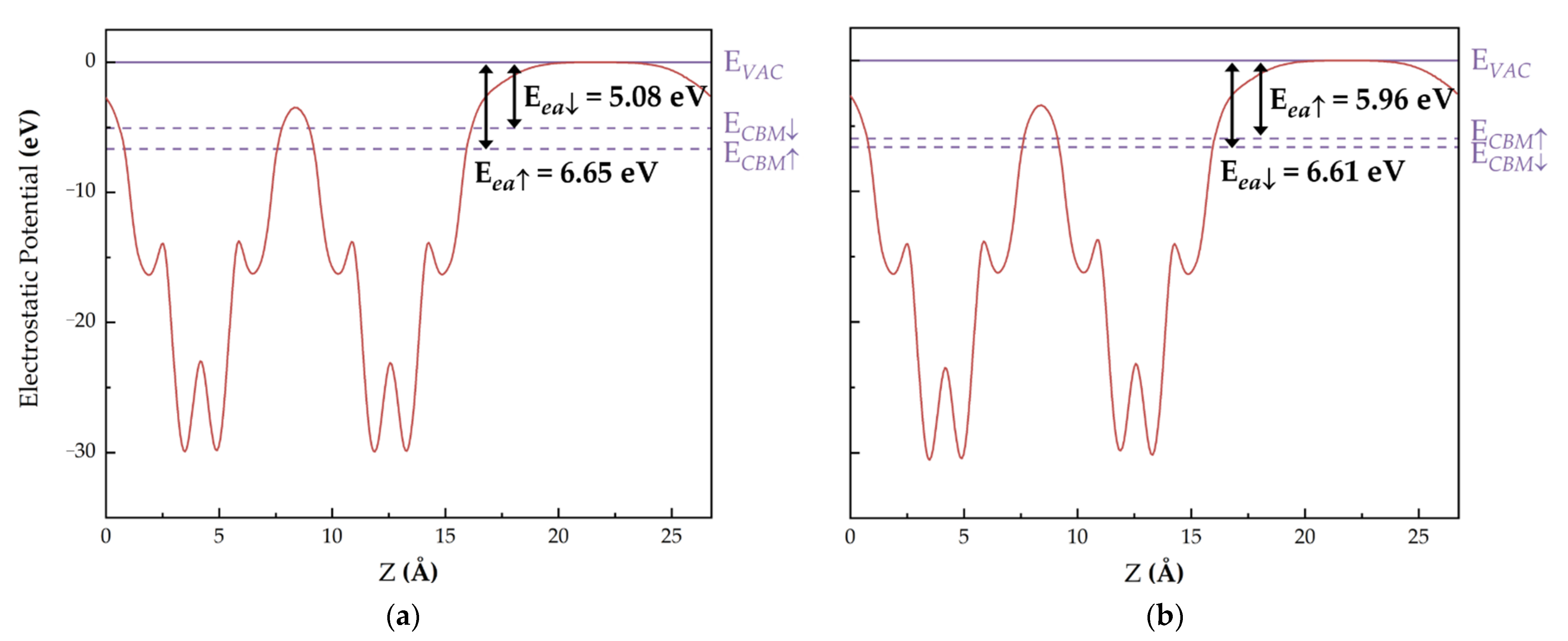
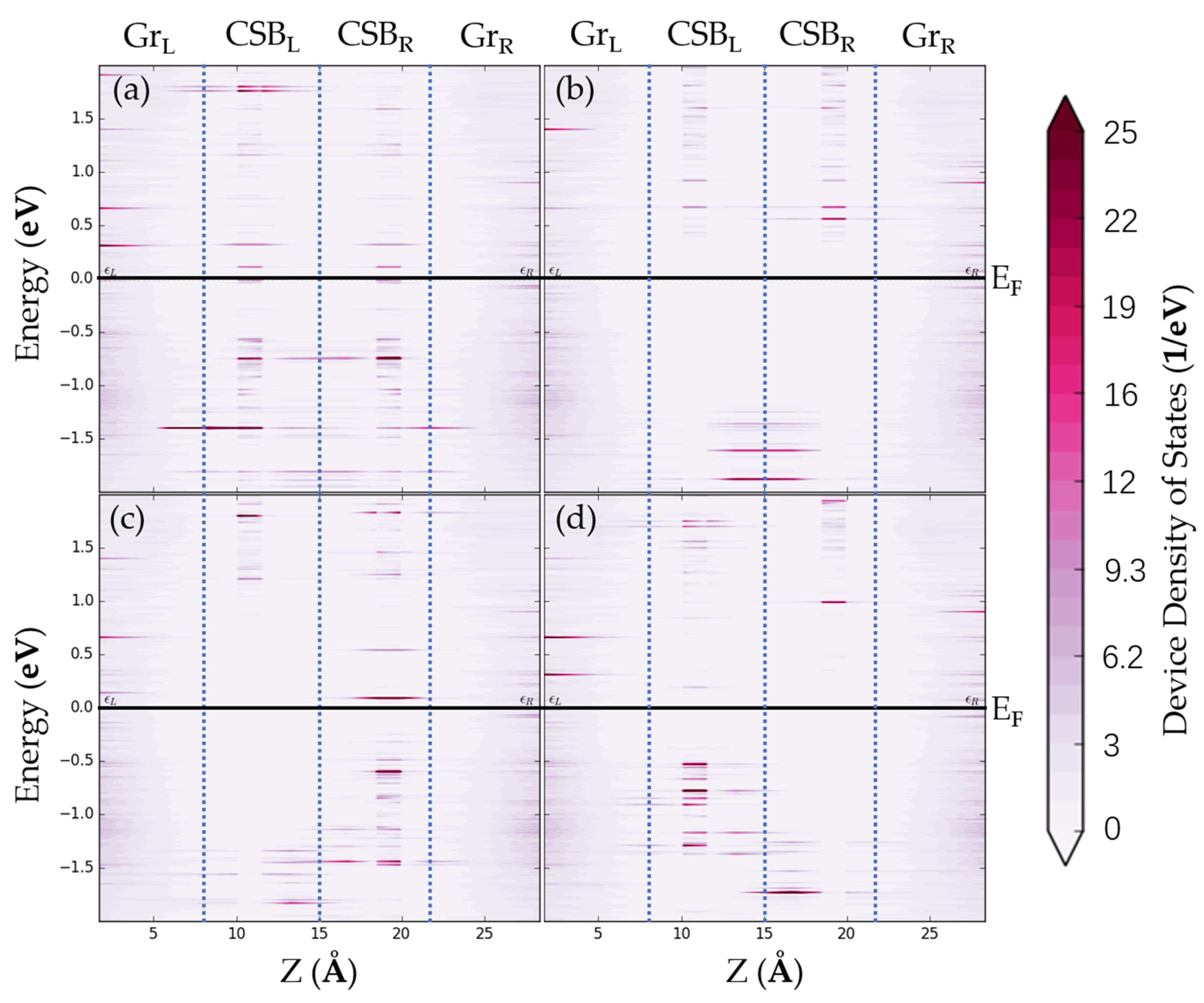
2. Results
3. Discussion
4. Materials and Methods
5. Conclusions
Author Contributions
Funding
Data Availability Statement
Conflicts of Interest
References
- Julliere, M. Tunneling between ferromagnetic films. Phys. Lett. A 1975, 54, 225–226. [Google Scholar] [CrossRef]
- Wolf, S.; Awschalom, D.; Buhrman, R.; Daughton, J.; Molnár, S.; Roukes, M.; Chtchelkanova, A.; Treger, D.M. Spintronics: A Spin-Based Electronics Vision for the Future. Science 2001, 294, 1488–1495. [Google Scholar] [CrossRef] [PubMed] [Green Version]
- Yang, S.; Zhang, J. Current Progress of Magnetoresistance Sensors. Chemosensors 2021, 9, 211. [Google Scholar] [CrossRef]
- Swagten, H.J.M.; Paluskar, P. Magnetic Tunnel Junctions. Mater. Today 2016, 9, 36–45. [Google Scholar]
- Baibich, M.; Broto, J.-M.; Fert, A.F.; F, N.; Petroff, F.; Etienne, P.E.; Creuzet, G.; Friederich, A.; Chazelas, J. Giant Magnetoresistance of (001)Fe/(001)Cr Magnetic Superlattices. Phys. Rev. Lett. 1988, 61, 2472–2475. [Google Scholar] [CrossRef] [Green Version]
- Ennen, I.; Kappe, D.; Rempel, T.; Glenske, C.; Hutten, A. Giant Magnetoresistance: Basic Concepts, Microstructure, Magnetic Interactions and Applications. Sensors 2016, 16, 904. [Google Scholar] [CrossRef]
- Dieny, B. Giant Magnetoresistance in Spin-Valve Multi-layers. J. Magn. Magn. Mater. 1994, 136, 335–359. [Google Scholar] [CrossRef]
- Svalov, A.V.; Savin, P.; Kurlyandskaya, G.; Gutierrez, J.; Barandiaran, J.M.; Vas’kovskiy, V.O. Spin-valve structures with Co-Tb-based multilayers. IEEE Trans. Magn. 2002, 38, 2782–2784. [Google Scholar] [CrossRef]
- Parkin, S. Giant Magnetoresistance in Magnetic Nanostructures. Annu. Rev. Mater. Sci. 2003, 25, 357–388. [Google Scholar] [CrossRef]
- Zheng, C.; Zhu, P.K.; Cardoso, S.; Chang, J.-Y.; Davies, J.; Eames, P.; Freitas, P.; Kazakova, O.; Kim, C.; Leung, C.-W.; et al. Magnetoresistive Sensor Development Roadmap (Non-Recording Applications). IEEE Trans. Magn. 2019, 55, 1–30. [Google Scholar] [CrossRef] [Green Version]
- Grabchikov, S.S.; Trukhanov, A.; Trukhanov, S.; Kazakevich, I.; Solobay, A.A.; Erofeenko, V.T.; Vasilenkov, N.V.; Volkova, O.S. Effectiveness of the magnetostatic shielding by the cylindrical shells. J. Magn. Magn. Mater. 2015, 398, 49–53. [Google Scholar] [CrossRef] [Green Version]
- Trukhanov, A.; Grabchikov, S.S.; Solobai, A.; Chushkova, D.; Trukhanov, S.; Trukhanova, E.L. AC and DC-shielding properties for the Ni80Fe20/Cu film structures. J. Magn. Magn. Mater. 2017, 443, 142–148. [Google Scholar] [CrossRef]
- Ajayan, P.; Kim, P.; Banerjee, K. Two-dimensional van der Waals materials. Phys. Today 2016, 69, 38–44. [Google Scholar] [CrossRef] [Green Version]
- Dayen, J.F.; Ray, S.; Karis, O.; Vera-Marun, I.; Kamalakar, M.V. Two-dimensional van der Waals spinterfaces and magnetic-interfaces. Appl. Phys. Rev. 2020, 7, 11303. [Google Scholar] [CrossRef] [Green Version]
- Ahn, E. 2D materials for spintronic devices. Npj 2D Mater. Appl. 2020, 4, 17. [Google Scholar] [CrossRef]
- Gong, C.; Li, L.; Li, Z.; Ji, H.; Stern, A.; Xia, Y.; Cao, T.; Bao, W.; Wang, C.; Wang, Y.; et al. Discovery of intrinsic ferromagnetism in two-dimensional van der Waals crystals. Nature 2017, 546, 265–269. [Google Scholar] [CrossRef] [PubMed] [Green Version]
- Huang, B.; Clark, G.; Navarro-Moratalla, E.; Klein, D.; Cheng, R.; Seyler, K.; Zhong, D.; Schmidgall, E.; McGuire, M.; Cobden, D.; et al. Layer-dependent Ferromagnetism in a van der Waals Crystal down to the Monolayer Limit. Nature 2017, 546, 270–273. [Google Scholar] [CrossRef] [Green Version]
- Deng, Y.; Yu, Y.; Song, Y.; Zhang, J.; Wang, N.; Wu, Y.; Zhu, J.; Wang, J.; Chen, X.; Zhang, Y. Gate-tunable Room-temperature Ferromagnetism in Two-dimensional Fe3GeTe2. Nature 2018, 563, 94–99. [Google Scholar] [CrossRef]
- Huang, Y.; Chen, W.; Wee, A. Two-dimensional magnetic transition metal chalcogenides. SmartMat 2021, 2, 139–153. [Google Scholar] [CrossRef]
- Loong, L.; Lee, W.; Qiu, X.; Yang, P.; Kawai, H.; Saeys, M.; Ahn, J.-H.; Yang, H. Flexible MgO Barrier Magnetic Tunnel Junctions. Adv. Mater. 2016, 28, 4983–4990. [Google Scholar] [CrossRef] [Green Version]
- Knudde, S.; Farinha, G.; Leitao, D.; Ferreira, R.; Cardoso, S.; Freitas, P. AlOx barrier growth in magnetic tunnel junctions for sensor applications. J. Magn. Magn. Mater. 2016, 412, 181–184. [Google Scholar] [CrossRef]
- Diao, Z.; Panchula, A.; Ding, Y.; Pakala, M.; Wang, S.; Li, Z.; Apalkov, D.; Nagai, H.; Driskill-Smith, A.; Wang, L.-C.; et al. Spin transfer switching in dual MgO magnetic tunnel junctions. Appl. Phys. Lett. 2007, 90, 132508. [Google Scholar] [CrossRef]
- Park, W.; Moon, K. Switchable Voltage Offset in a Heusler Alloy-based Magnetic Tunnel Junction. J. Magn. Magn. Mater. 2018, 469, 274–278. [Google Scholar] [CrossRef]
- Lu, H.; Robertson, J.; Naganuma, H. Comparison of hexagonal boron nitride and MgO tunnel barriers in Fe, Co magnetic tunnel junctions. Appl. Phys. Rev. 2021, 8, 31307. [Google Scholar] [CrossRef]
- Yuasa, S.; Djayaprawira, D. Giant tunnel magnetoresistance in magnetic tunnel junctions with a crystalline MgO(001) barrier. J. Phys. D Appl. Phys. 2007, 40, 337–354. [Google Scholar] [CrossRef] [Green Version]
- Worledge, D.; Geballe, T. Magnetoresistive double spin filter tunnel junction. J. Appl. Phys. 2000, 88, 5277–5279. [Google Scholar] [CrossRef]
- Miao, G.-X.; Müller, M.; Moodera, J. Magnetoresistance in Double Spin Filter Tunnel Junctions with Nonmagnetic Electrodes and its Unconventional Bias Dependence. Phys. Rev. Lett. 2009, 102, 76601. [Google Scholar] [CrossRef] [PubMed]
- Song, T.; Cai, X.; Tu, W.-Y.; Zhang, X.; Huang, B.; Wilson, N.; Seyler, K.; Zhu, L.; Taniguchi, T.; Watanabe, K.; et al. Giant Tunneling Magnetoresistance in Spin-Filter van der Waals Heterostructures. Science 2018, 360, 1214–1218. [Google Scholar] [CrossRef] [Green Version]
- Jin, W.; Kim, H.; Ye, Z.; Li, S.; Rezaie, P.; Diaz, F.; Siddiq, S.; Wauer, E.; Yang, B.; Chenghe, L.; et al. Raman fingerprint of two terahertz spin wave branches in a two-dimensional honeycomb Ising ferromagnet. Nat. Commun. 2018, 9, 5122. [Google Scholar] [CrossRef] [Green Version]
- Rahman, S.; Torres, J.F.; Khan, A.; Lu, Y. Recent Developments in van der Waals Antiferromagnetic 2D Materials: Synthesis, Characterization, and Device Implementation. ACS Nano 2021, 15, 17175–17213. [Google Scholar] [CrossRef]
- Parkin, S.; Kaiser, C.; Panchula, A.; Rice, P.; Hughes, B.; Samant, M.; Yang, S.-H. Giant Tunneling Magnetoresistance at Room Temperature with MgO(100) Tunnel Barriers. Nat. Mater. 2005, 3, 862–867. [Google Scholar] [CrossRef] [PubMed]
- McGuire, M.; Clark, G.; Santosh, K.; Chance, W.; Jellison, G.E., Jr.; Cooper, V.; Xu, X.; Sales, B. Magnetic Behavior and Spin-Lattice Coupling in Cleavable, van der Waals Layered CrCl3 Crystals. Phys. Rev. Mater. 2017, 1, 14001. [Google Scholar] [CrossRef]
- Zhang, S.; Wang, R.; Wang, X.; Wei, B.; Chen, B.; Wang, H.; Shi, G.; Wang, F.; Jia, B.; Ouyang, Y.; et al. Experimental Observation of the Gate-Controlled Reversal of the Anomalous Hall Effect in the Intrinsic Magnetic Topological Insulator MnBi2Te4 Device. Nano Lett. 2019, 20, 709714. [Google Scholar] [CrossRef] [PubMed] [Green Version]
- Huang, X.; Tang, Y.; Dong, S. Strain-engineered A-type antiferromagnetic order in YTiO3: A first-principles calculation. J. Appl. Phys. 2013, 113, 17E108. [Google Scholar] [CrossRef] [Green Version]
- Telford, E.; Dismukes, A.; Lee, K.; Cheng, M.; Wieteska, A.; Bartholomew, A.; Chen, Y.-S.; Xu, X.; Pasupathy, A.; Zhu, X.; et al. Layered Antiferromagnetism Induces Large Negative Magnetoresistance in the van der Waals Semiconductor CrSBr. Adv. Mater. 2020, 32, 2003240. [Google Scholar] [CrossRef]
- Zubar, T.; Fedosyuk, V.; Trukhanov, S.; Chushkova, D.; Michels, D.; Lyakhov, D.; Trukhanov, A. Method of surface energy investigation by lateral AFM: Application to control growth mechanism of nanostructured NiFe films. Sci. Rep. 2020, 10, 14411. [Google Scholar] [CrossRef]
- Sharko, S.; Serokurova, A.; Novitskii, N.; Ketsko, V.; Smirnova, M.; Almuqrin, A.; Trukhanov, S.; Trukhanov, A. A New Approach to the Formation of Nanosized Gold and Beryllium Films by Ion-Beam Sputtering Deposition. Nanomaterials 2022, 12, 470. [Google Scholar] [CrossRef]
- Jiang, Z.; Wang, P.; Xing, J.; Jiang, X.; Zhao, J. Screening and Design of Novel 2D Ferromagnetic Materials with High Curie Temperature above Room Temperature. ACS Appl. Mater. Interfaces 2018, 10, 39032–39039. [Google Scholar] [CrossRef]
- Ye, C.; Wang, C.; Wu, Q.; Liu, S.; Zhou, J.; Wang, G.; Söll, A.; Sofer, Z.; Yue, M.; Liu, X.; et al. Layer-Dependent Interlayer Antiferromagnetic Spin Reorientation in Air-Stable Semiconductor CrSBr. ACS Nano, 2022; in press. [Google Scholar] [CrossRef]
- Trukhanov, S.; Trukhanov, A.; Turchenko, V.; Trukhanov, A.V.; Chushkova, D.; Trukhanova, E.L.; Ivanov, V.M.; Salem, M.; Kostishyn, V.G.; Panina, L.; et al. Polarization origin and iron positions in indium doped barium hexaferrites. Ceram. Int. 2017, 44, 290–300. [Google Scholar] [CrossRef]
- Turchenko, V.; Trukhanov, S.; Kostishin, V.; Damay, F.; Porcher, F.; Klygach, D.; Vakhitov, M.; Matzui, L.; Yakovenko, O.; Bozzo, B.; et al. Impact of In3+ cations on structure and electromagnetic state of M-type hexaferrites. J. Energy Chem. 2021, 69, 667–676. [Google Scholar] [CrossRef]
- Huang, B.; McGuire, M.; May, A.; Xiao, D.; Jarillo-Herrero, P.; Xu, X. Emergent phenomena and proximity effects in two-dimensional magnets and heterostructures. Nat. Mater. 2020, 19, 1276–1289. [Google Scholar] [CrossRef] [PubMed]
- Wang, H.; Qi, J.; Qian, X. Electrically tunable high Curie temperature two-dimensional ferromagnetism in van der Waals layered crystals. Appl. Phys. Lett. 2020, 117, 83102. [Google Scholar] [CrossRef]
- Grimme, S.; Antony, J.; Ehrlich, S.; Krieg, H. A Consistent and Accurate Ab Initio Parametrization of Density Functional Dispersion Correction (DFT-D) for the 94 Elements H-Pu. J. Chem. Phys. 2010, 132, 154104. [Google Scholar] [CrossRef] [PubMed] [Green Version]
- Troyanchuk, I.; Trukhanov, S.; Shapovalova, E.; Khomchenko, V.; Tovar, M.; Szymczak, H. The influence of oxygen vacancies on the magnetic state of La0.50D0.50MnO3−γ (D = Da, Sr) manganites. J. Exp. Theor. Phys. 2003, 96, 1055–1064. [Google Scholar] [CrossRef]
- Trukhanov, S.; Bushinsky, M.; Troyanchuk, I.; Szymczak, H. Magnetic ordering in La1−xSrxMnO3−x/2 anion-deficient manganites. J. Exp. Theor. Phys. 2004, 99, 756–765. [Google Scholar] [CrossRef]
- Tiusan, C.; Greullet, F.; Hehn, M.; Montaigne, F.; Andrieu, S.; Schuhl, A. Spin tunnelling phenomena in single-crystal magnetic tunnel junction systems. J. Phys. Condens. Matter. 2007, 19, 165201. [Google Scholar] [CrossRef]
- Stewart, D. New Type of Magnetic Tunnel Junction Based on Spin Filtering through a Reduced Symmetry Oxide: FeCo|Mg3B2O6|FeCo. Nano Lett. 2009, 10, 263–267. [Google Scholar] [CrossRef]
- Heyd, J.; Scuseria, G.E.; Ernzerhof, M. Hybrid functionals based on a screened Coulomb potential. J. Chem. Phys. 2006, 124, 8207–8215. [Google Scholar] [CrossRef] [Green Version]
- Smidstrup, S.; Markussen, T.; Vancraeyveld, P.; Wellendorff, J.; Schneider, J.; Gunst, T.; Verstichel, B.; Stradi, D.; Khomyakov, P.; Vej-Hansen, U.; et al. QuantumATK: An integrated platform of electronic and atomic-scale modelling tools. J. Phys. Condens. Matter. 2019, 32, 15901. [Google Scholar] [CrossRef]
- Kresse, G.; Furthmüller, J. Efficient iterative schemes for ab initio total-energy calculations using a plane-wave basis set. Phys. Rev. B 1996, 55, 11169–11174. [Google Scholar] [CrossRef] [PubMed]
- Blöchl, P. Projector Agmented-Wave Method. Phys. Rev. B 1994, 50, 17953–17979. [Google Scholar] [CrossRef] [PubMed] [Green Version]
- Perdew, J.; Burke, K.; Ernzerhof, M. Generalized Gradient Approximation Made Simple. Phys. Rev. Lett. 1996, 77, 3865–3868. [Google Scholar] [CrossRef] [PubMed] [Green Version]
- Smidstrup, S.; Stradi, D.; Wellendorff, J.; Khomyakov, P.; Vej-Hansen, U.; Lee, M.-E.; Ghosh, T.; Jónsson, E.; Jonsson, H.; Stokbro, K. First-principles Green’s-function method for surface calculations: A pseudopotential localized basis set approach. Phys. Rev. B 2017, 96, 195309. [Google Scholar] [CrossRef] [Green Version]
- Marmolejo-Tejada, J.; Dolui, K.; Lazic, P.; Chang, P.-H.; Smidstrup, S.; Stradi, D.; Stokbro, K.; Nikolic, B. Proximity Band Structure and Spin Textures on Both Sides of Topological-Insulator/Ferromagnetic-Metal Interface and Their Charge Transport Probes. Nano Lett. 2017, 17, 5626–5633. [Google Scholar] [CrossRef] [Green Version]
- Brandbyge, M.; Mozos, J.-L.; Ordejon, P.; Taylor, J.; Stokbro, K. Density-functional method for nonequilibrium electron transport. Phys. Rev. B 2001, 65, 165401. [Google Scholar] [CrossRef] [Green Version]


| Number of CrSBr Layers | TMR | ||
|---|---|---|---|
| 2 | 4.35 × 10⁻¹⁰ | 1.01 × 10⁻¹⁰ | 3.3 × 10²% |
| 4 | 1.87 × 10⁻¹² | 9.19 × 10⁻¹⁸ | 2.0 × 10⁷% |
| 6 | 7.52 × 10⁻¹⁴ | 6.86 × 10⁻¹⁷ | 1.1 × 10⁵% |
Publisher’s Note: MDPI stays neutral with regard to jurisdictional claims in published maps and institutional affiliations. |
© 2022 by the authors. Licensee MDPI, Basel, Switzerland. This article is an open access article distributed under the terms and conditions of the Creative Commons Attribution (CC BY) license (https://creativecommons.org/licenses/by/4.0/).
Share and Cite
Liu, H.; Liu, Y.-Y.; Wen, H.; Wu, H.; Zong, Y.; Xia, J.; Wei, Z. Spin-Filter Magnetic Tunnel Junctions Based on A-Type Antiferromagnetic CrSBr with Giant Tunnel Magnetoresistance. Magnetochemistry 2022, 8, 89. https://doi.org/10.3390/magnetochemistry8080089
Liu H, Liu Y-Y, Wen H, Wu H, Zong Y, Xia J, Wei Z. Spin-Filter Magnetic Tunnel Junctions Based on A-Type Antiferromagnetic CrSBr with Giant Tunnel Magnetoresistance. Magnetochemistry. 2022; 8(8):89. https://doi.org/10.3390/magnetochemistry8080089
Chicago/Turabian StyleLiu, Hao, Yue-Yang Liu, Hongyu Wen, Haibin Wu, Yixin Zong, Jianbai Xia, and Zhongming Wei. 2022. "Spin-Filter Magnetic Tunnel Junctions Based on A-Type Antiferromagnetic CrSBr with Giant Tunnel Magnetoresistance" Magnetochemistry 8, no. 8: 89. https://doi.org/10.3390/magnetochemistry8080089