Article

Microstructures of the Activated Si-Containing AB2 Metal Hydride Alloy Surface by Transmission Electron Microscope

1
BASF/Battery Materials-Ovonic, 2983 Waterview Drive, Rochester Hills, MI 48309, USA
2
Department of Chemical Engineering and Materials Science, Wayne State University, Detroit, MI 48202, USA
*
Author to whom correspondence should be addressed.
Batteries 2016, 2(1), 4; https://doi.org/10.3390/batteries2010004
Submission received: 13 December 2015 / Revised: 27 February 2016 / Accepted: 29 February 2016 / Published: 7 March 2016
(This article belongs to the Special Issue Nickel Metal Hydride Batteries)

Abstract

:
The surface microstructure of an activated Si-containing AB2 metal hydride (MH) alloy was investigated by transmission electron microscopy (TEM) and X-ray energy dispersive spectroscopy (EDS). Regions of the main AB2 and the secondary TiNi (B2 structure) phases directly underneath the surface Zr oxide/hydroxide layers are considered electrochemically inactive. The surface of AB2 is covered, on the atomic scale, by sheets of Ni2O3 with direct access to electrolyte and voids, without the buffer oxide commonly seen in Si-free AB2 alloys. This clean oxide/bulk metal alloy interface is believed to be the main source of the improvements in the low-temperature performance of Si-containing AB2 alloys. Sporadic metallic-Ni clusters can be found in the surface Ni2O3 region. However, the density of these clusters is much lower than the Ni-inclusions found in most typical metal hydride surface oxides. A high density of nano-sized metallic Ni-inclusions (1–3 nm) is found in regions associated with the TiNi secondary phase, i.e., in the surface oxide layer and in the grain boundary, which can also contribute to enhancement of the electrochemical performance.

Graphical Abstract

1. Introduction

Sales of hybrid electrical vehicles (HEV), which are mainly based on the nickel/metal hydride (Ni/MH) battery technology, passed 10 million in July 2015 [1]. With a fast charge/discharge capability [2,3], a long cycle stability [4], high efficiency under a large charge current [5], superb abuse tolerance [6,7], and a wide operation temperature range [8,9], Ni/MH batteries are expected to power HEV for another decade. Therefore, efforts to improve the performance of Ni/MH batteries have never stopped. Ni/MH batteries have a catalytic oxide layer on the anode surface that facilitates the electrochemical reaction with the electrolyte, which is similar to the solid-electrolyte-interface (SEI) formation on the anode surface of a Li-ion battery [10,11,12,13,14,15,16]. In a conventional AB2 metal hydride (MH) alloy, the catalytic surface oxide is composed of (1) a buffer oxide layer (approximately 100 nm and 50 nm for AB2 and AB5, respectively) on top of the metal bulk, followed by (2) a porous oxide layer (approximately 200 nm and 100 nm for AB2 and AB5, respectively), and finally (3) a surface oxide layer that is electrochemical inactive [17]. The porous surface oxide and metallic inclusions (mainly Ni) of several common AB2 and AB5 MH alloys have been studied by transmission electron microscopy (TEM) [13,14,15,16,17,18,19,20,21,22,23,24,25,26], electron energy loss spectroscopy (EELS) [17,27], X-ray diffraction (XRD) [28], X-ray photoemission spectroscopy (XPS) [29], and magnetic susceptibility measurements [26,30,31,32,33]. The general conclusion is that the metallic Ni inclusions embedded in the supportive oxides are the key catalyst for the electrochemical reaction in Ni/MH batteries.
Si-addition in a typical Laves phase based MH alloy demonstrated a large decrease in charge-transfer resistance at both room temperature and −40 °C [34], which was attributed to increased catalytic ability in the main C14 phase. Although both the abundances of the C15 and TiNi (B2 structure) secondary phases are higher in the Si-containing AB2 alloy, their content remains relatively small (≤5 wt%). AC impedance results showed that both the surface area and surface catalytic ability increases with the incorporation of Si. The increase in the former was attributed to the higher solubility of Si oxide, whereas the origin of the increase in the latter remains unclear [34]. A similar enhancement in electrochemical reactivity with Si and AB2 MH alloys was also previously reported [35], but the mechanism of the improvement is also not available. TEM has been used extensively to study the multi-phase nature of AB2 MH alloys [36,37,38,39,40], as well as the surface oxides of conventional AB2 and AB5 MH alloys [17,26]. Therefore, in this study, we applied TEM techniques to reveal the detailed microstructure of the activated Si-containing AB2 MH alloy surface.

2. Experimental Section

Arc melting of the designed alloy samples was performed with a non-consumable tungsten electrode and water-cooled copper tray, under a continuous argon flow. A piece of sacrificial titanium underwent several melting-cooling cycles before each run to reduce residual systemic oxygen levels. Each 12-g ingot sample was re-melted and turned over several times to ensure a uniform chemical composition. A JEOL-JSM6320F scanning electron microscope (SEM, JEOL, Tokyo, Japan) with X-ray energy dispersive spectroscopy (EDS) capabilities was used to study the phase distribution and composition of the as-cast ingots [34]. Ingots were hydrided, de-hydrided, crushed, and ground to powder and then sieved through a 200-mesh sieve. The final powder was etched in 100 °C 30% KOH for 4 h (h) to emulate a lightly cycled electrode [17,26,30]. TEM examination was performed with a CM200/FEG microscope (Philips, Amsterdam, The Netherlands). The operating voltage was 200 keV. Magnetic susceptibility was measured using a Digital Measurement Systems Model 880 vibrating sample magnetometer (MicroSense, Lowell, MA, USA).
TEM sample preparation included the following steps:
(1)
Mixing of the powders with M-Bond 610 glue, followed by placement of the mixture into a 3 mm diameter copper pipe. This was then cured for 8 h at 150 °C;
(2)
Slicing the copper pipe containing the glued powders into 0.5 mm thick disks using a low-speed diamond saw;
(3)
Polishing of the 3-mm-diameter disk down to approximately 100 µm using SiC media from 320 grit down to 1200 grit, then dimpling grinding;
(4)
Finishing of thinning with 5 kV ion milling (on a liquid N2 cooled stage);
(5)
Finally, insertion of the sample into the microscope to examine for electron beam transparency areas. If none are detected, additional ion milling time, followed by TEM examination, is required. This step was repeated as many times as necessary to provide high quality thin areas for detailed TEM studies.

3. Results and Discussion

3.1. Summary of Alloy Properties

While the surface microstructure of the Si-free AB2 MH alloy has been fully investigated in our previous paper [17], a Si4 alloy with a designed composition of Ti12Zr21.5V10Cr7.5Mn8.1Co8.0Ni28.2Si4.0Sn0.3Al0.4 from a previous report on the effects of Si-incorporation in the Laves phase based AB2 MH alloy [34] was selected for this TEM/EDS study. Based on the full-phase analysis of the XRD data, this alloy (Si4) contained a major C14 phase (92.0 wt%), a C15 secondary phase (5.0 wt%), and a TiNi—like B2 secondary phase (3.0 wt%). EDS analysis showed that the Si-contents in C14, C15, and B2 (TiNi) phase were 3.2–5.5 at%, 1.6–1.9 at%, and 0.2 at%, respectively. Compared to the Si-free base alloy Si0, the Si4 alloy has a larger unit cell, higher C15 and B2 secondary phase abundances, a lower pressure-concentration-temperature (PCT) plateau pressure, a larger PCT hysteresis, a smaller gaseous phase and electrochemical storage capacities, a higher hydrogen diffusion coefficient, a higher surface exchange current, a lower charge transfer resistance and a higher surface reactive area as measured at −40 °C, and a higher surface catalytic ability [34].

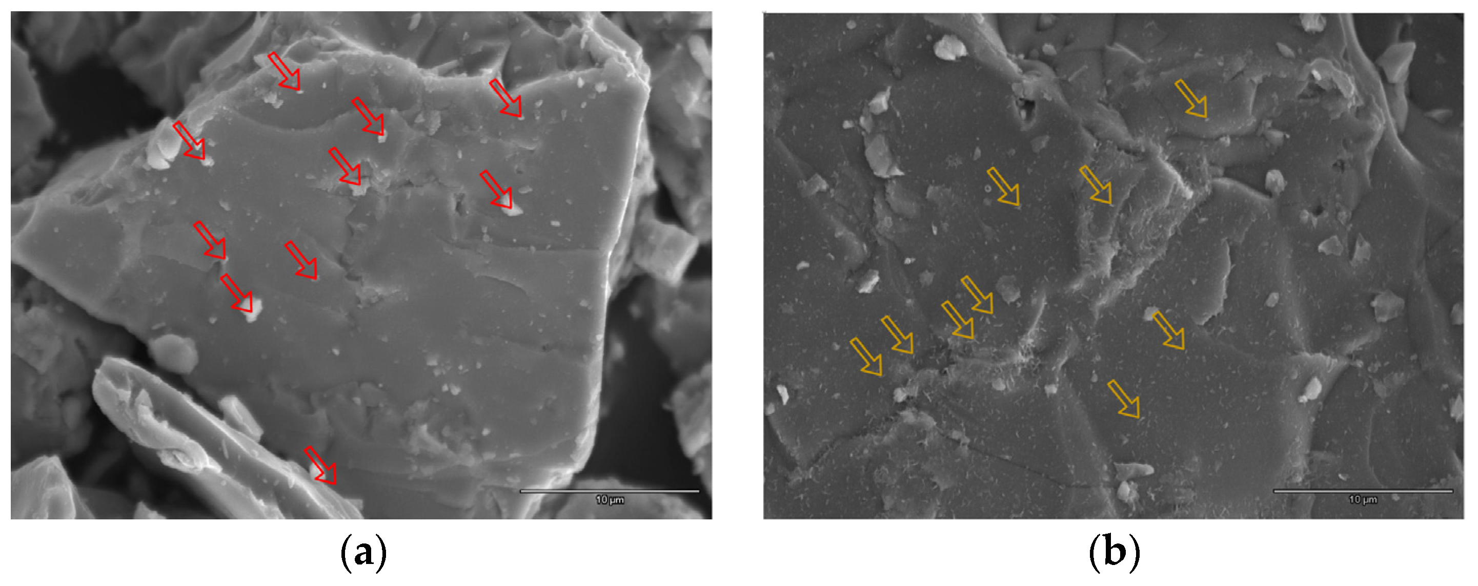
3.2. Scanning Electron Microscope and X-Ray Energy Dispersive Spectroscopy Analyses on the Activated Alloy Surface

Both the pristine and activated alloy powder surfaces were examined by SEM and the resulting secondary electron images are shown in Figure 1a,b, respectively. Some fine particles seen on the surface of the pristine alloy are believed to be dust from hydrogenation and grinding operations. Interestingly, additional fine needle structures are observed on the activated alloy surface (Figure 1b). TEM studies indicated that these needles are mainly Zr oxide/hydroxide. The composition of the activated alloy surface was measured by EDS, although only semi-quantitative, and is in agreement with that of design (Table 1). The similar EDS results between design and etched samples indicate that the alloy surface affected by the activation procedure is much shallower than the X-ray escape depth of the EDS technique (typically 1–2 μm).

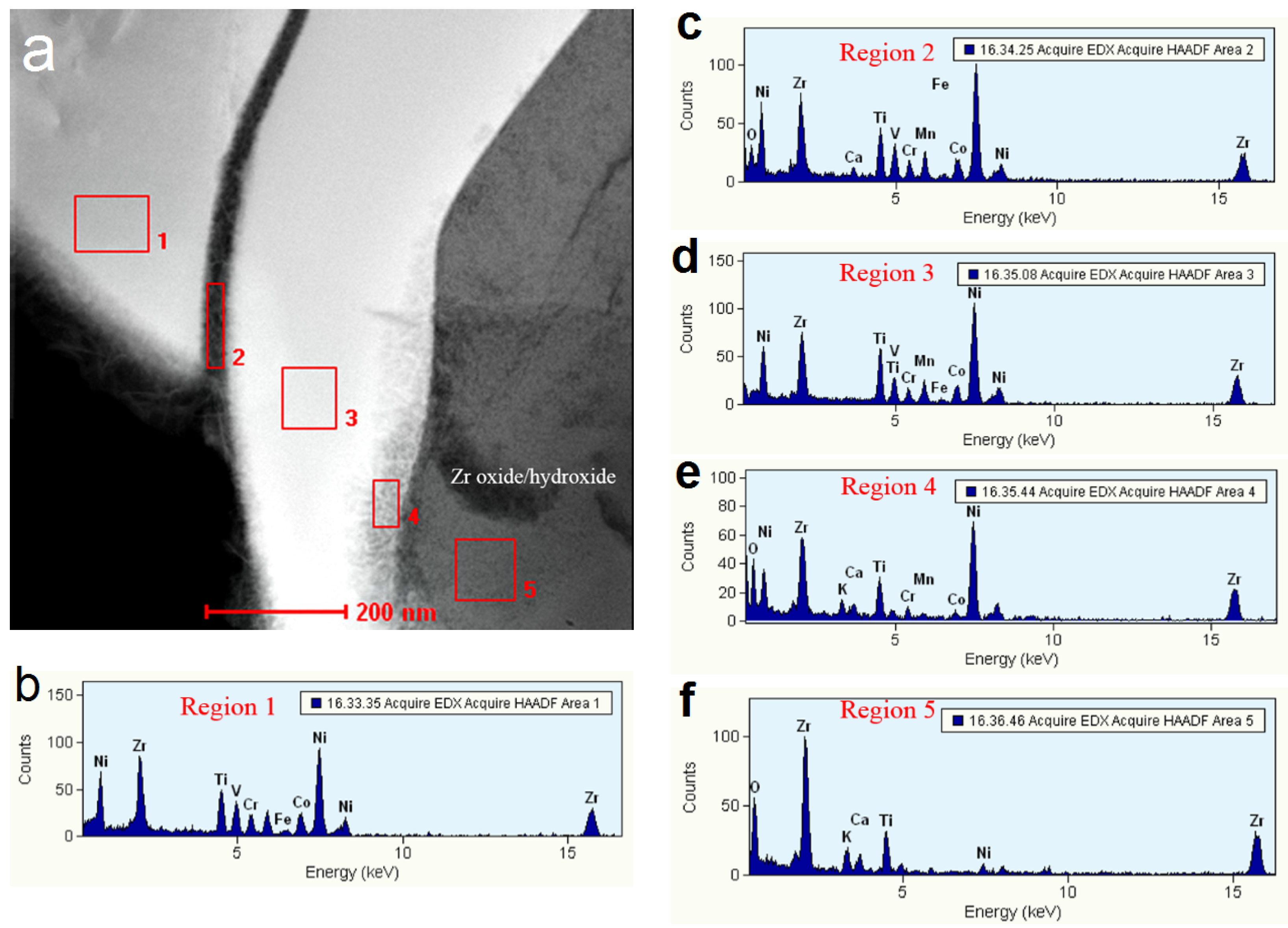
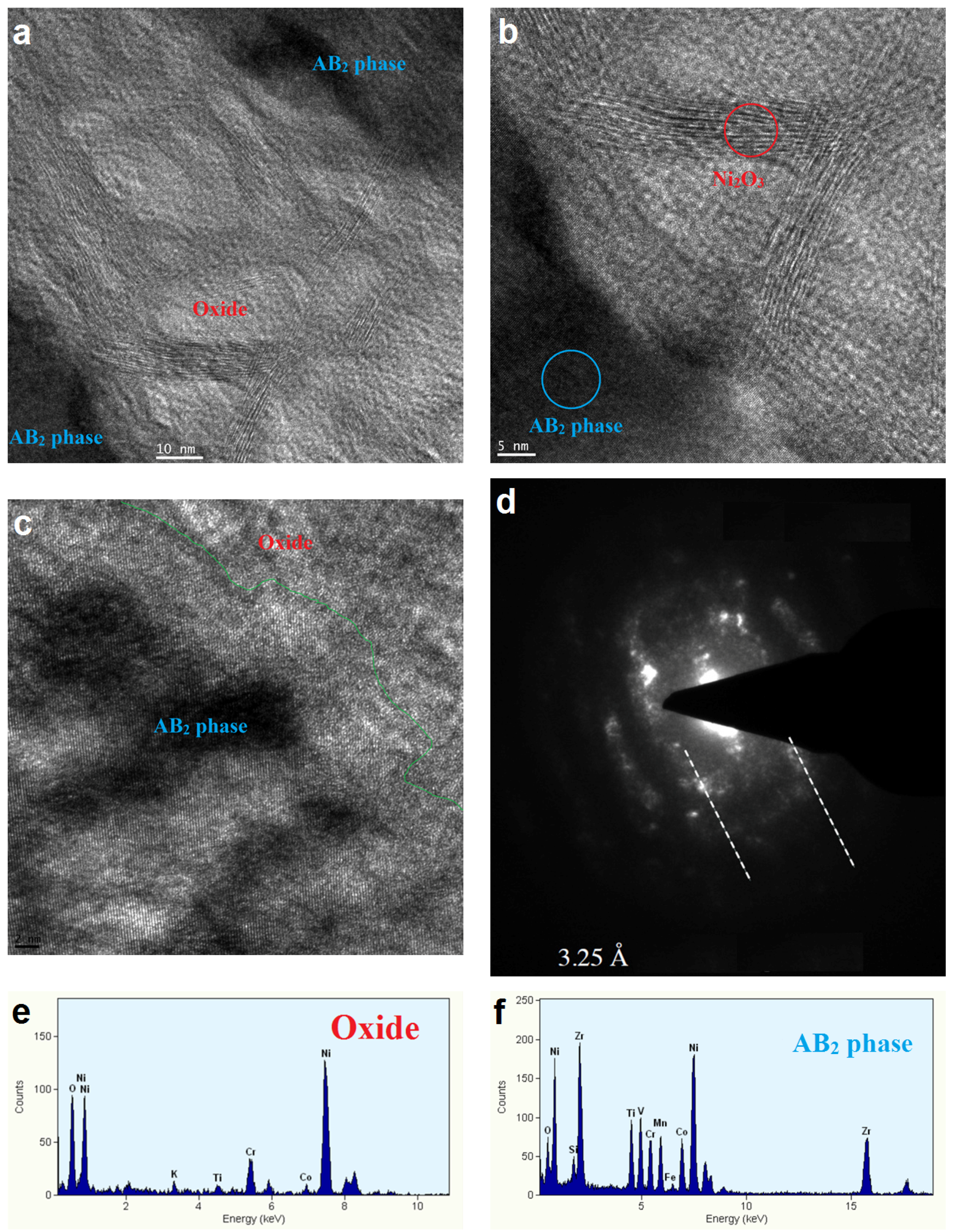
3.3. Regions under the Zr Oxide/Hydroxide Layer

Figure 2a is a TEM bright field (BF) micrograph from a region containing two typical AB2 crystals under the Zr oxide/hydroxide layer. Because of variations in sample thicknesses and weak EDS spectrum signal, resulting from a very small volume, composition calculations based on the TEM/EDS are much more challenging (if even possible) than those in SEM/EDS. Therefore, in this paper, semi-quantitative analyses were only carried out on several representative EDS spectra and most of the EDS spectra were qualitatively compared without delving into inaccessible quantitative details. EDS spectra recorded from the five numbered red box regions in Figure 2a are displayed in Figure 2b–f. The EDS spectra of Regions 1 (Figure 2b) and 3 (Figure 2d), which exhibit all expected elements of design with no detectable O signal, are assigned to the metallic AB2 bulk phase. The EDS spectrum of Region 2 showed a similar metal content to the AB2 bulk (Figure 2b,d) with an additional miniscule amount of oxygen signal. The observed Ca signal is due to artifacts from contamination during sample preparation. Figure 2e represents an EDS spectrum recorded from Region 4, the surface of the AB2 phase, specifically heavily oxidized Zr, Ti, and Ni, some K from the etching solution, and very small amounts of V, Cr, and Mn. The spectrum is qualitatively similar to the buffer oxide in the previously reported activated Si-free AB2 MH alloy surface [17]. Metallic Ni-inclusions were not visible in this region. The EDS spectrum (Figure 2f) of the top most surface represents mostly Zr and O, with smaller amounts of Ti, K, and Ni. The O/Zr atomic ratio in this region was estimated to be approximately 2.7, which is between the ratios of ZrO2 (2.0) and ZrO2·2H2O or Zr(OH)4 (4.0), and is closer to the former. This is the reason why this region was designated as a Zr oxide/hydroxide. With a surface oxide/hydroxide covering the entire surface and no metallic Ni embedded in the supporting oxide, the AB2 region directly beneath the surface oxide is considered electrochemically inactive and cannot be the source of the improved low-temperature performance.
A TEM BF micrograph taken from a different region shows three bright contrast areas in Figure 3a. Two are marked with A and one is marked with B. In addition to a dark contrast area on the left side of B, a crack clearly separates Areas A and B. Small cracks and fissures are normally generated during the hydrogenation and grinding processes. The EDS spectra from Areas A and B are shown in Figure 3b,c, respectively. Both spectra show no trace of O and a full compositional analysis (in at%) are presented in Table 2. According to the composition measurements, Areas A and B were identified as AB2 and B2 phases, respectively. In summary: the AB2 phase contains all the elements in the composition; the B2 phase consists mainly of Ti, Zr, Ni, and Co. Low solubilities of V, Cr, and Mn in the B2 phase are in agreement with a previous report [33] and almost all the Si resides in the AB2 phase.
Further EDS spectra from the B2 phase and the dark contrast area will be discussed below in Figure 4. Figure 4a is a high-magnification TEM BF micrograph focusing on the bottom left corner of the B2 crystal and its surrounding areas. EDS examination was carried out in the following six areas: Region 1 represents the surface oxide/hydroxide, Region 2 shows the B2 bulk crystal (the same B2 crystal shown in Figure 3a), and Regions 3–6 are in the regions between B2 and surface oxide/hydroxide and the boundary areas surrounding the B2 phase. The corresponding EDS spectra are shown in Figure 4b–g. The EDS spectrum of Region 1 (Figure 4b) is very similar to that shown in Figure 2f representing a typical Zr oxide/hydroxide feature. The O/Zr ratios in the Zr oxide/hydroxide surface for both the AB2 and B2 phases are very similar. Meanwhile, the EDS spectrum of Region 2—very similar to the one displayed in Figure 3c—is considered to represent the bulk of metallic B2 phase, and those from Regions 3–5 are hypothesized to be buffer oxide with high Ni-content. Region 6, a region next to an activated grain boundary, also shows a similar spectrum, but with an even higher Ni-content. No metallic Ni-inclusions were found in the region of the B2 phase under the surface oxide. This is similar to the AB2 phase under the Zr oxide/hydroxide. Judging from the high packing density of the surface Zr oxide/hydroxide, the region of the B2 phase under the same oxide is not electrochemically active.

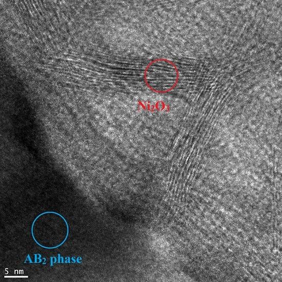
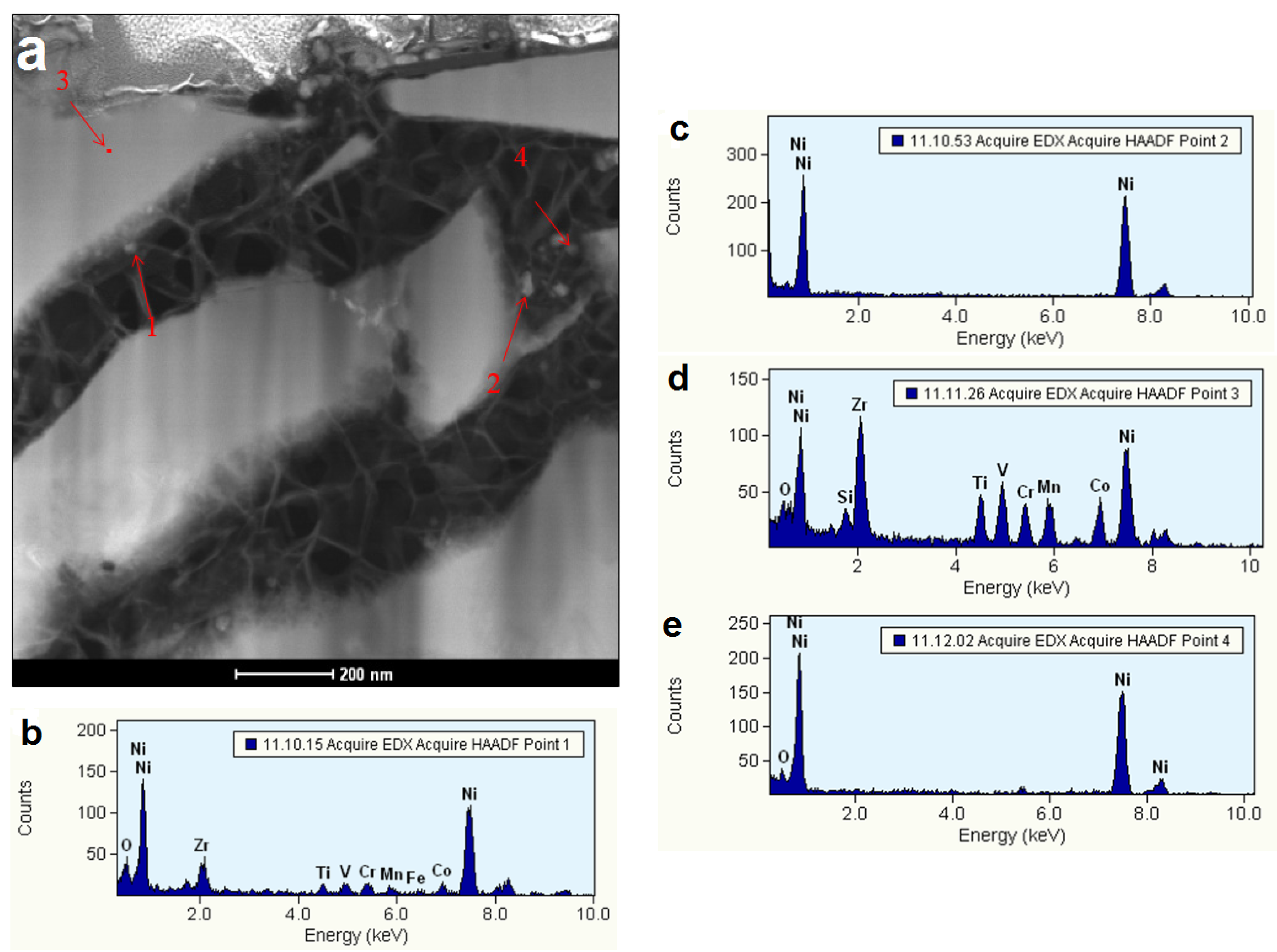
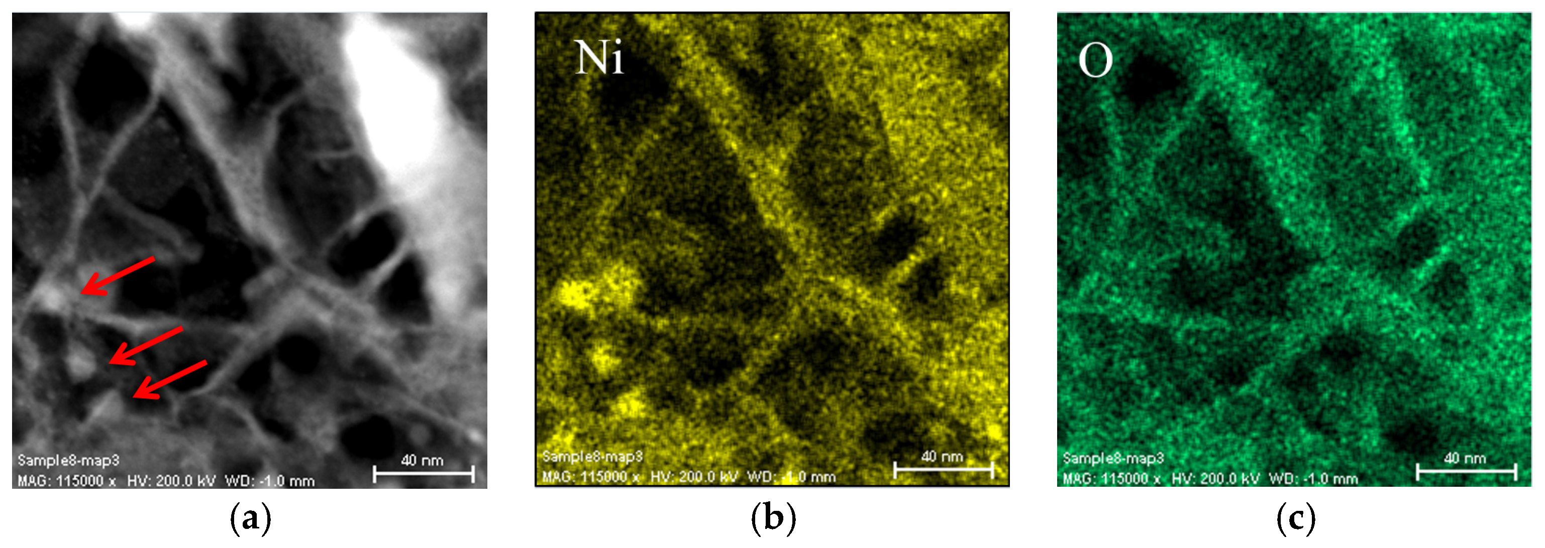
3.4. Electrochemically Active Surfaces on the AB2 Phase

Figure 5a is a TEM BF micrograph showing open space areas filled with fibrous-like microstructures near the middle portion of the view. A red rectangular region marked at the bottom edge of an open area (surface oxide) was closely examined by TEM BF micrography in higher magnification, shown in Figure 5b. The EDS spectra recorded from Areas 1–3 are present in Figure 5c–e, respectively. Area 1 contains mainly Ni oxide/hydroxide with small amounts of Cr, Zr, Ti, Mn, Si, and K (from the etching solution). Both Areas 2 and 3 are composed of partial oxides from all the metallic components and the oxygen signal intensity in Area 2 is higher than that in Area 3. In both areas, while the overall compositions are similar to that of the AB2 phase (Figure 2b), the Ni-contents are significantly higher. This area can be considered as the surface oxide region of AB2 phase, under the Ni oxide/hydroxide layer.
The fine microstructure of the Ni oxide/hydroxide-AB2 phase interface was further investigated with high resolution (HR) TEM. A representative HR-TEM micrograph in Figure 6a shows an oxide region sandwiched between two AB2 metal alloy grains. The central portion is filled with a high density of fibrous-like features, similar to the oxide formation found in La-addition AB2 metal alloys [26]. A higher magnification micrograph of the same region clearly shows layered structures associated with oxide formation (Figure 6b). Finally, the atomic fringes of the AB2 crystal are clearly visible in Figure 6c. These atomic fringes have an average inter-planar distance of 0.24 nm, which is close to the (200) plane of a C14 structure. The interface between the oxide and AB2 metal alloy bulk crystal (green line) is very clean and free of any amorphous phase, as is the buffer oxide layer reported earlier [17]. A selective area electron diffraction pattern (SAD) in the oxide region is shown in Figure 6f. The lattice spacing, calibrated with a Pd foil, is 0.325 nm, which is very close to the (101) inter-planar distance of 0.323 nm for a Ni2O3 crystal [41]. The compositions of the oxide and AB2 phases were studied by EDS and the resulting spectra are shown in Figure 6e,f. The oxide area has an O/Ni ratio slightly higher than the stoichiometric 1.5 in Ni2O3, contains some Cr, possibly traces of Co, Ti, and no detectable Si. Therefore, this region is mainly Ni oxide with a small amount of Ni(OH)2. The composition of the AB2 alloy crystal is very close to the one found in the bulk (Figure 3b) with a small amount of oxygen, which suggests that a small portion of the AB2 phase was oxidized. In summary, the region of AB2 directly underneath the Ni2O3 sheets, which contain voids, is slightly oxidized and has direct access to the electrolyte and, therefore, is considered electrochemically active.
The surface Ni oxide region examined more thoroughly by TEM is shown in a regular TEM BF micrograph (Figure 7a), where some bright particles, marked by red arrows 1, 2, and 4, are present in the surface Ni oxide/hydroxide region. The composition of the four red arrow points shown in Figure 7a were examined by EDS and the resulting spectra are displayed in Figure 7b–e. Point 1 indicates a mixture of Ni and AB2 phase with some degree of oxidation (Figure 7b). Points 2 and 4 are pure metallic Ni clusters. Point 3 exhibits a typical AB2 composition. The Ni metallic inclusions are known to facilitate electrochemical reactions when they are imbedded in the surface porous oxide [30]. We believe the metallic Ni-clusters (10–20 nm) found here may not play an important role in the electrochemical reaction because of their relatively low density, when compared to the typical Ni inclusion in the supportive oxide on the conventional MH alloys.
The Ni-inclusions were studied further using TEM micrography combined with EDS mappings. There are three clusters, each with a diameter of approximately 10 nm, denoted by red arrows in Figure 8a. The corresponding Ni- and O-mappings in the same area indicate that these three particles are made of Ni without any O and are therefore metallic Ni. Besides the Ni-inclusions in the region, the Ni-mapping coincides with O-mapping very well in the remaining areas, which signify that the surface of AB2 phase in this region is covered mostly by Ni oxide/hydroxide.
Magnetic susceptibility measurements were used to quantify the total amount of metallic Ni on the surface, using the saturated magnetic susceptibility (MS) and the average magnetic domain size, which is reversely proportional to the magnetic field strength at one-half of the MS value (H1/2). Details of the measurement protocol can be found in our earlier publications [30,33]. According to the results shown in Table 3, the Si-containing Si5 AB2 MH alloy has a slightly lower total amount of metallic Ni, with a similar average Ni cluster size to those in the Si-free Si0 alloy. Therefore, the enhancement in the low-temperature performance with the addition of Si in the formula cannot be linked to metallic Ni-clusters. When compared to other AB5 and A2B7 in Table 3, the AB2 alloys have an insufficient amount of surface metallic Ni-that too small in size, which, therefore, increases in the surface catalytic ability by other means is extremely critical for improving the electrochemical performance of AB2 MH alloys.

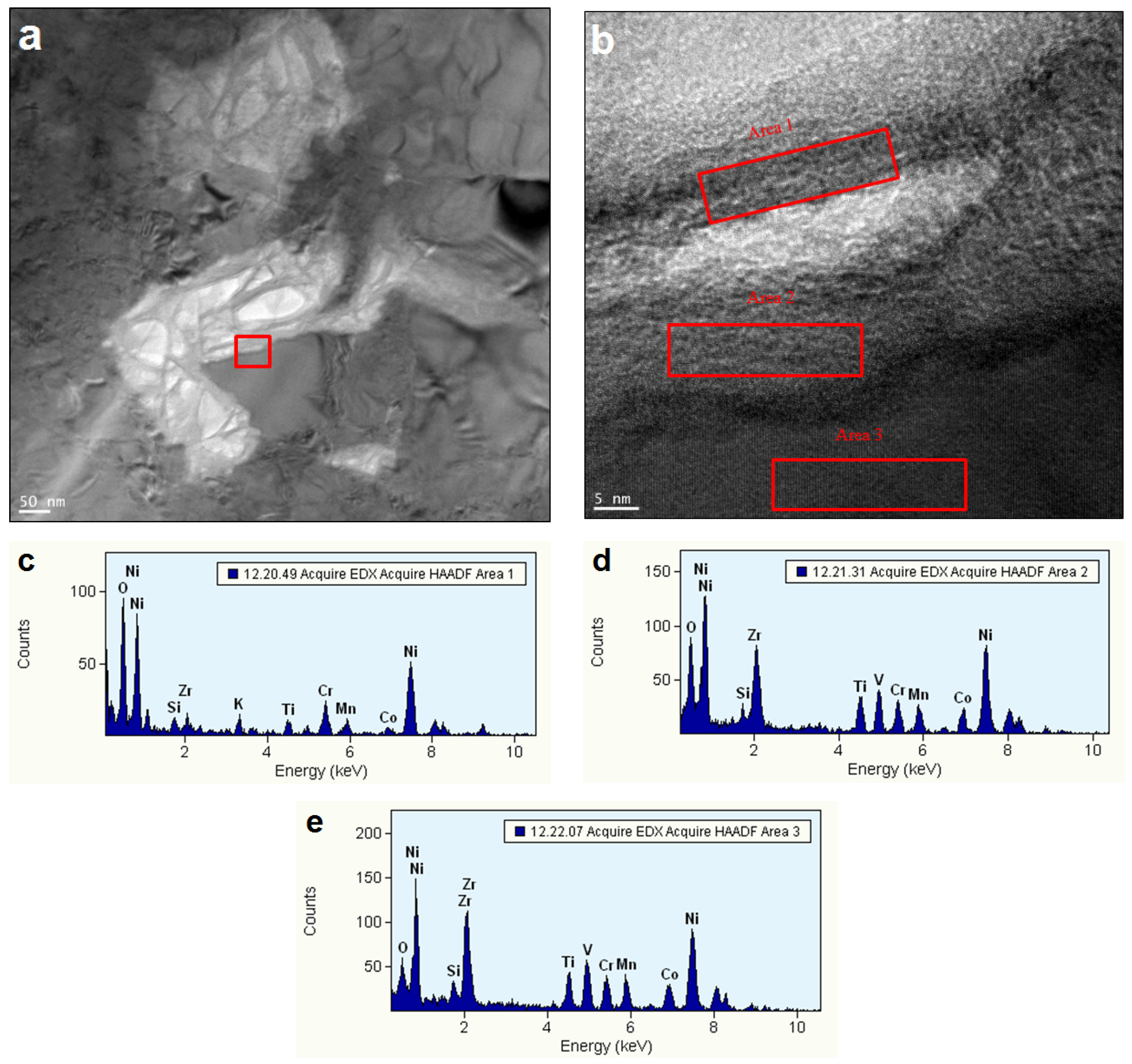
3.5. Electrochemically Active Surfaces on the B2 Phase

The B2 phase, only 3.0 wt% of Si4, can also be an electrochemical active component in the AB2 MH alloy [42,43]. A TEM BF micrograph in Figure 9a shows that the same surface of B2 phase was not entirely covered by the thick Zr oxide/hydroxide, as addressed in Section 3.3. The EDS spectra taken from the areas marked as 1, 2, 3, and 4 are shown in Figure 9b–e, respectively. The spectrum of Area 1 shows a typical element-distribution of a B2 phase (refer to Figure 3c). Area 2 contains mainly Ni and O with an O/Ni ratio of roughly 0.7, which suggest a mixture of metallic Ni and Ni oxide. The composition in Area 3 approaches a fully oxidized Ni oxide, while Area 4 may be a mix of metal (Zr, Ti, and Ni) oxides. From the structure, Region 2 is proposed to be the catalyst for the electrochemical reaction.
A catalytic mixture of Ni metal/oxide can also be found in the activated (etched) grain boundary between two B2 phase grains, as shown in the TEM BF micrograph in Figure 10a. In this case, the grain boundary region reacts rapidly with the KOH electrolyte, particularly with the connected voids, to remove the oxidation products and replace them with fresh electrolyte. The three square numbered areas were analyzed by EDS and the resulting spectra are shown in Figure 10b–d. Both grains (Areas 1 and 2) are assigned to the B2 phase, but with different compositions; while Square 1 shows a typical bulk B2 composition (Figure 3c), Square 2 has higher Zr and Sn content and a smaller Ti content. The dark spot in the grain boundary between two B2 crystals shows a high-Ni level and some degree of oxidation of Zr and Ti (Figure 10d). An HR-TEM BF image with an inserted SAD pattern is shown in Figure 10e. The micrograph is filled by the nano-scaled crystallites (~2 nm in diameter), attributing to the continuous halo-like rings in the SAD pattern. The ring patterns represent the face-centered cubic structure of the material. Among them, the most intense pattern corresponds to a lattice spacing of 0.21 nm, which results from the metallic Ni (111) plane. Figure 10f is a slightly lower magnification TEM dark field (DF) micrograph from the same area. The observed bright spots are the Ni nano-crystallites that are the dominating component in this area.
Another HR-TEM BF micrograph demonstrating the presence of oxide in the B2 phase grain boundary is shown in Figure 11a with the corresponding EDS mappings of Ni (Figure 11b) and O (Figure 11c). Different from what is shown in Figure 8, the Ni-mapping in Figure 11a–c complements the O-mapping, suggesting a high density of metallic-Ni on the B2 phase surface.

4. Conclusions

With a detailed TEM/EDS study, the surfaces of the main AB2 phases not covered by Zr oxide/hydroxide are identified as the main source of improvement in low-temperature electrochemical performance. The electrolyte interface is a porous open space filled with fibrous Ni oxide sheets. The metal/oxide interface is free from amorphous buffer oxide, which can substantially reduce charge-transfer resistance. The surface of the B2 phase not directly under the Zr oxide/hydroxide is also electrochemically active, but the significance to the improvement is considered of secondary order because of the small percentage (3.0 wt%) and lack of Si, which is very common in Si-free AB2 MH alloys. In contrast with the conventional MH alloys, the surface embedded metallic Ni nano-particles in the AB2 phase in the Si-containing alloys, with a relatively low density, do not contribute directly to the improvement in the low-temperature performance of the MH alloys.

Acknowledgments

The authors would like to thank the following individuals from BASF-Ovonic for their help: Benjamin Reichman, Benjamin Chao, Baoquan Huang, Diana F. Wong, Taihei Ouchi, David Pawlik, Allen Chan, Ryan J. Blankenship, and Su Cronogue.

Author Contributions

Kwo-hsiung Young designed and conduct the experiment. Benjamin Chao and Jean Nei helped in the data interpretation and manuscript preparation.

Conflicts of Interest

The authors declare no conflict of interest.

References

  1. Hybrid Electric Vehicle. Available online: https://en.wikipedia.org/wiki/Hybrid_electric_vehicle (accessed on 30 August 2015).
  2. Takasaki, T.; Nishimura, K.; Saito, M.; Fukunaga, H.; Iwaki, T.; Sakai, T. Cobalt-free nickel–metal hydride battery for industrial applications. J. Alloys Compd. 2013, 580, S378–S381. [Google Scholar] [CrossRef]
  3. Nishimura, K.; Takasaki, T.; Sakai, T. Introduction of large-sized nickel–metal hydride battery GIGACELL® for industrial applications. J. Alloys Compd. 2013, 580, S353–S358. [Google Scholar] [CrossRef]
  4. Kai, T.; Ishida, J.; Yasuoka, S.; Takeno, K. The effect of nickel-metal hydride battery’s characteristics with structure of the alloy. In Proceedings of the 54th Battery Symposium in Japan, Osaka, Japan, 6–9 October 2013; p. 210.
  5. Kang, J.; Yan, F.; Zhang, P.; Du, C. Comparison of comprehensive properties of Ni-MH (nickel-metal hydride) and Li-ion (lithium-ion) batteries in terms of energy efficiency. Energy 2014, 70, 618–625. [Google Scholar] [CrossRef]
  6. Ovshisnky, S.R.; Fetcenko, M.A.; Ross, J. A nickel metal hydride battery for electric vehicles. Science 1993, 260, 176–181. [Google Scholar]
  7. Dhar, S.K.; Ovshinsky, S.R.; Gifford, P.R.; Corrigan, D.A.; Fetcenko, M.A.; Venkatesan, S. Nickel/metal hydride technology for consumer and electric vehicle batteries—A review and up-date. J. Power Sources 1997, 65, 1–7. [Google Scholar] [CrossRef]
  8. Fierro, C.; Zallen, A.; Koch, K.; Fetcenko, M.A. The influence of nickel-hydroxide composition and microstructure on the high-temperature performance of nickel metal hydride batteries. J. Electrochem. Soc. 2006, 153, A492–A496. [Google Scholar] [CrossRef]
  9. Fetcenko, M.A.; Ovshinsky, S.R.; Reichman, B.; Young, K.; Fierro, C.; Koch, J.; Zallen, A.; Mays, W.; Ouchi, T. Recent advances in NiMH battery technology. J. Power Sources 2007, 165, 544–551. [Google Scholar] [CrossRef]
  10. Kong, F.; Kostecki, R.; Nadeau, G.; Song, X.; Zaghib, K.; Kinoshita, K.; McLarnon, F. In situ studies of SEI formation. J. Power Sources 2001, 97–98, 58–66. [Google Scholar] [CrossRef]
  11. Vetter, J.; Novák, P.; Wagner, M.R.; Veit, C.; Möller, K.-C.; Besenhard, J.O.; Winter, M.; Wohlfahrt-Mehrens, M.; Vogler, C.; Hammouche, A. Ageing mechanisms in lithium-ion batteries. J. Power Sources 2005, 147, 269–281. [Google Scholar] [CrossRef]
  12. Zhang, S.S. A review on electrolyte additives for lithium-ion batteries. J. Power Sources 2006, 162, 1379–1394. [Google Scholar] [CrossRef]
  13. Schranzhofer, H.; Bugajski, J.; Santner, H.J.; Korepp, C.; Möller, K.-C.; Besenhard, J.O.; Winter, M.; Sitte, W. Electrochemical impedance spectroscopy study of the SEI formation on graphite and metal electrodes. J. Power Sources 2006, 153, 391–395. [Google Scholar] [CrossRef]
  14. Bryngelsson, H.; Stjerndahl, M.; Gustafsson, T.; Edström, K. How dynamic is the SEI? J. Power Sources 2007, 174, 970–975. [Google Scholar] [CrossRef]
  15. Kim, S.; van Duin, A.C.T.; Shenoy, V.B. Effect of electrolytes on the structure and evolution of the solid electrolyte interphase (SEI) in Li-ion batteries: A molecular dynamics study. J. Power Sources 2011, 196, 8590–8597. [Google Scholar] [CrossRef]
  16. Colclasure, A.M.; Smith, K.A.; Kee, R.J. Modeling detailed chemistry and transport for solid-electrolyte-interface (SEI) films in Li–ion batteries. Electrochim. Acta 2011, 58, 33–43. [Google Scholar] [CrossRef]
  17. Young, K.; Chao, B.; Liu, Y.; Nei, J. Microstructures of the oxides on the activated AB2 and AB5 metal hydride alloys surface. J. Alloys Compd. 2014, 606, 97–104. [Google Scholar] [CrossRef]
  18. Schlapbach, L.; Stucki, F.; Seiler, A.; Siegmann, H.C. The formation of superparamagnetic metallic Ni and Fe particles at the surface of intermetallics by surface segregation. Surf. Sci. 1981, 106, 157–159. [Google Scholar] [CrossRef]
  19. Stucki, F.; Schlapbach, L. Magnetic properties of LaNi5, FeTi, Mg2Ni and their hydrides. J. Less Comm. Metal. 1980, 74, 143–151. [Google Scholar] [CrossRef]
  20. Stucki, F. Surface analysis by magnetization measurements on FeTi and Fe0.85Mn0.15Ti. J. Appl. Phys. 1982, 53, 2643–2644. [Google Scholar] [CrossRef]
  21. Kim, G.; Chun, C.; Lee, S.; Lee, J. A study on the microstructural change of surface of the intermetallic compound LaNi5 by hydrogen absorption. Scr. Metall. Mater. 1993, 29, 485–490. [Google Scholar] [CrossRef]
  22. Broom, D.P.; Kemali, M.; Ross, D.K. Magnetic properties of commercial metal hydride battery materials. J. Alloys Compd. 1999, 293–295, 255–259. [Google Scholar] [CrossRef]
  23. Tai, L.T.; Hang, B.T.; Thuy, N.P.; Hieh, T.D. Magnetic properties of LaNi5-based compounds. J. Magn. Magn. Mater. 2003, 262, 485–489. [Google Scholar] [CrossRef]
  24. Termsuksawad, P.; Niyomsoan, S.; Goldfarb, R.B.; Kaydanov, V.I.; Olson, D.L.; Mishra, B.; Gavra, Z. Measurement of hydrogen in alloys by magnetic and electronic techniques. J. Alloys Compd. 2004, 373, 86–95. [Google Scholar] [CrossRef]
  25. Li, W.K.; Ikeda, K.; Nakamori, Y.; Orimo, S.; Yakushiji, K.; Takanashi, K.; Ohyama, H.; Nakatsuji, K.; Dansui, Y. Size distribution of precipitated Ni clusters on the surface of an alkaline-treated LaNi5-based alloy. Acta Mater. 2007, 55, 481–485. [Google Scholar] [CrossRef]
  26. Young, K.; Chao, B.; Pawlik, D.; Shen, H. Transmission electron microscope studies in the surface oxide on the La-containing AB2 metal hydride alloy. J. Alloys Compd. 2016. [Google Scholar] [CrossRef]
  27. Fetcenko, M.A.; Ovshinsky, S.R.; Young, K.; Reichman, B.; Fierro, C.; Koch, J.; Mays, W.; Ouchi, T.; Sommers, B.; Zallen, A. High catalytic activity disordered VTiZrNiCrCoMnAlSn hydrogen storage alloys for nickel–metal hydride batteries. J. Alloys Compd. 2002, 330–332, 752–759. [Google Scholar] [CrossRef]
  28. Maurel, F.; Knosp, B.; Backhaus-Ricoult, M. Characterization of corrosion products of AB5-type hydrogen storage alloys for nickel-metal hydride batteries. J. Electrochem. Soc. 2000, 147, 78–86. [Google Scholar] [CrossRef]
  29. Song, D.; Gao, X.; Zhang, Y.; Lin, D.; Zhou, Z.; Wang, G.; Shen, P. Surface analysis of a TiNiB hydrogen storage electrode. J. Alloys Compd. 1993, 199, 161–163. [Google Scholar]
  30. Young, K.; Huang, B.; Regmi, R.K.; Lawes, G.; Liu, Y. Comparisons of metallic clusters imbedded in the surface oxide of AB2, AB5, and A2B7 alloys. J. Alloys Compd. 2010, 506, 831–840. [Google Scholar] [CrossRef]
  31. Young, K.; Nei, J. The Current Status of Hydrogen Storage Alloy Development for Electrochemical Applications. Materials 2013, 6, 4574–4608. [Google Scholar] [CrossRef]
  32. Young, K.; Nei, J.; Wong, D.F.; Wang, L. Structural, hydrogen storage, and electrochemical properties of Laves phase-related body-centered-cubic solid solution metal hydride alloys. Int. J. Hydrog. Energy 2014, 39, 21489–21499. [Google Scholar] [CrossRef]
  33. Wong, D.F.; Young, K.; Nei, J.; Wang, L.; Ng, K.Y.S. Effects of Nd-addition on the structural, hydrogen storage, and electrochemical properties of C14 metal hydride alloys. J. Alloys Compd. 2015, 647, 507–518. [Google Scholar] [CrossRef]
  34. Young, K.; Ouchi, T.; Huang, B.; Reichman, B.; Blankenship, R. Improvement in −40 °C electrochemical properties of AB2 metal hydride alloy by silicon incorporation. J. Alloys Compd. 2013, 575, 65–72. [Google Scholar] [CrossRef]
  35. Chen, J.; Dou, S.X.; Bradhurst, D.; Liu, H.K. Nickel Hydroxide as an Active Material for the Positive Electrode in Rechargeable Alkaline Batteries. In Proceedings of the Twelfth Annual Battery Conference on Applications and Advances, Long Beach, CA, USA, 14–17 January 1997; IEEE: Piscataway, NJ, USA, 1997; pp. 313–316. [Google Scholar]
  36. Song, X.; Zhang, Z.; Zhang, X.B.; Lei, Y.Q.; Wang, Q.D. Effect of Ti Substitution on the microstructure and properties of Zr–Mn–V–Ni AB2 type hydride electrode alloys. J. Mater. Res. 1999, 14, 1279–1285. [Google Scholar] [CrossRef]
  37. Shi, Z.; Chumbley, S.; Laabs, F.C. Electron diffraction analysis of an AB2-type Laves phase for hydrogen battery applications. J. Alloys Compd. 2000, 312, 41–52. [Google Scholar] [CrossRef]
  38. Song, X.; Chen, Y.; Sequeira, C.; Zhang, Z. Microstructural evolution of body-centered cubic structure related Ti–Zr–Ni phases in non-stoichiometric Zr-based Zr–Ti–Mn–V–Ni hydride electrode alloys. J. Mater. Res. 2003, 18, 37–44. [Google Scholar] [CrossRef]
  39. Boettinger, W.J.; Newbury, D.E.; Wang, K.; Bendersky, L.A.; Chiu, C.; Kattner, U.R.; Young, K.; Chao, B. Examination of Multiphase (Zr,Ti)(V,Cr,Mn,Ni)2 Ni-MH Electrode Alloys: Part I. Dendritic Solidification Structure. Metall. Mater. Trans. A 2010, 41, 2033–2047. [Google Scholar] [CrossRef]
  40. Bendersky, L.A.; Wang, K.; Boettinger, W.J.; Newbury, D.E.; Young, K.; Chao, B. Examination of Multiphase (Zr,Ti)(V,Cr,Mn,Ni)2 Ni-MH Electrode Alloys: Part II. Solid-State Transformation of the Interdendritic B2 Phase. Metall. Mater. Trans. A 2010, 41, 1891–1906. [Google Scholar] [CrossRef]
  41. Powder Diffraction File (PDF) Database; MSDS No. 00-014-0481; International Centre for Diffraction Data: Newtown Square, PA, USA, 2011.
  42. Young, K.; Reichman, B.; Fetcenko, M.A. Electrochemical performance of AB2 metal hydride alloys measured at −40 °C. J. Alloys Compd. 2013, 580, S349–S352. [Google Scholar] [CrossRef]
  43. Young, K.; Wong, D.F.; Nei, J.; Reichman, B. Electrochemical properties of hypo-stoichiometric Y-doped AB2 metal hydride alloys at ultra-low temperature. J. Alloys Compd. 2015, 643, 17–27. [Google Scholar] [CrossRef]
Figure 1. Scanning electron microscope (SEM) micrographs showing the surfaces of (a) pristine and (b) activated Si4 alloy. While dust particles on the pristine surface (a few examples indicated by red arrows) are from the pulverization/grinding operation, smaller sized precipitations of Zr oxide/hydroxide can be seen on the activated surface (representative examples indicated by yellow arrow).
Batteries 02 00004 g001
Figure 2. (a) A transmission electron microscopy (TEM) bright field (BF) micrograph showing the region representative of the AB2 phase underneath the surface Zr oxide/hydroxide and (b)–(f) the corresponding EDS spectra from Areas 1–5.
Batteries 02 00004 g002
Figure 3. (a) A TEM BF micrograph and the corresponding EDS spectra from (b) Area A (AB2 phase) and (c) Area B (B2 phase).
Batteries 02 00004 g003
Figure 4. (a) A higher magnification TEM BF micrograph of Figure 3a, showing the B2 phase underneath the surface Zr oxide/hydroxide and (b)–(g) the corresponding EDS spectra from Areas 1–6.
Batteries 02 00004 g004
Figure 5. (a) A TEM BF micrograph showing the interface between oxide/AB2 phases; (b) a higher magnification image from the red box region shown in (a); and (c)–(e) the associative EDS spectra from areas identified in (b).
Batteries 02 00004 g005
Figure 6. (a) A TEM BF micrograph showing the oxide between two AB2 crystals; (b) a higher magnification image of one interface; (c) a clean interface image showing lattice fringes of 0.24 nm inter-planar spacing for the AB2 crystal (200) plane and the oxide; (d) a SAD pattern from the oxide region showing an inter-planar distance of 0.325 nm and EDS spectra recorded from (e) the corresponding oxide and (f) AB2 phase areas.
Batteries 02 00004 g006
Figure 7. (a) A TEM BF micrograph showing surface oxide and imbedded Ni-clusters and (b)–(e) the corresponding EDS spectra from the areas identified in (a).
Batteries 02 00004 g007
Figure 8. (a) A TEM BF micrograph showing three metallic Ni-clusters, indicated by arrows, in the oxide on the AB2 phase surface, and EDS mappings of (b) Ni and (c) O.
Batteries 02 00004 g008
Figure 9. (a) A TEM BF micrograph showing the oxide on the B2 phase surface and (b)–(e) the corresponding EDS spectra from the areas identified in (a).
Batteries 02 00004 g009
Figure 10. (a) A TEM BF micrograph showing the oxide between two B2 phases; (b)–(d) the corresponding EDS spectra from the areas identified in (a); (e) a high magnification TEM BF image with a SAD in the insert (e); and (f) a TEM DF micrograph from the same region as (e) showing the dominant Ni nano-crystallites.
Batteries 02 00004 g010
Figure 11. (a) A TEM BF micrograph showing oxide on the B2 phase surface, and EDS mappings of (b) Ni and (c) O. Different from Figure 8, the Ni-mapping here is complementary to the O-mapping, suggesting a high density of metallic-Ni on the B2 phase surface.
Batteries 02 00004 g011
Table 1. Design and surface composition of activated alloy Si4 determined by SEM-X-ray energy dispersive spectroscopy (EDS). All numbers are in at%.
OriginAlSiTiVCrMnCoNiZrSn
Design0.44.012.010.07.58.18.028.221.50.3
Surface0.74.211.210.17.58.48.229.320.30.1
Table 2. EDS results from two phases identified by TEM BF micrography in Figure 3a. All numbers are in at%. ND denotes not detectable.
LocationAlSiTiVCrMnCoNiZr
Area A (AB2 phase)1.255.239.7713.0612.479.868.6023.5916.12
Area B (B2 phase)ND0.1924.081.08ND0.786.9347.4019.52
Table 3. Comparison of saturated magnetic susceptibility (MS) and applied magnetic field, corresponding to half of MS (H1/2), for Si-free Si0 and Si-containing Si5 AB2, AB5 and some A2B7 MH alloys. Mm stands for Ce-free misch metal.
PropertiesSi5-AB2Si0-AB2AB5La-A2B7Nd-A2B7Mm-A2B7
MS in emu·g−10.03240.03720.4340.3690.6790.314
H1/2 in kOe0.4510.4930.1730.1250.1020.128
ReferencesThis work[33][30][30]Nd-AB5[31]

