1. Introduction
The phenomenon of stress buildup during film deposition on substrates has been known for many years. In particular, the role of these residual stresses in applications using film/substrate systems such as microelectronic devices and manufacturing cutting tools may be dramatic, leading to device failure or protective properties’ modifications. Thin films are often under compressive stresses [
1], especially when sputtering deposition techniques are applied.
Increasing the thickness of the compressed thin film leads to an increase in the total elastic energy stored in the film, which is often locally relaxed through the appearance of damage, such as wrinkles or blisters, and subsequent fractures or spalling for brittle materials when stresses reach high values. Indeed, it is well known that buckling of thin film is linked to elastic instability that releases stresses in the film. Wrinkles generated in thin films have been studied by several authors [
2,
3,
4,
5,
6,
7]. Theoretical and numerical calculations based on Föpple–Von Karman equations have been performed for several typical modes (straight-sided wrinkle, telephone cord wrinkle, circular blister) [
6,
8,
9,
10]. However, these equations cannot be used in more complex topologies where several buckles exist in one macroscopic region of the thin film. Furthermore, correlative studies of the veracity and trend of the distribution of experimental stresses, with theoretical or numerical analysis of buckling patterns after the delamination of thin films, are less common. This means that numerical stress prediction or experimental stress measurements of complex buckling patterns at the micron scale are still open questions [
11,
12]. It is therefore important to determine the effective stress field associated with local damages. However, determination of residual stresses in thin films is often performed experimentally over the global film surface, mapping of the local stress distribution being rarely performed for metallic films [
13].
At the macroscopic scale, the residual stresses obtained by X-ray diffraction were compared to the simulation results from finite elements method (FEM) for the case of small deformations [
14]. However, the microscopic sizes of the buckles have so far prevented direct measurement of strain and stress distributions over the buckling region to support these theoretical and numerical results. Wafer curvature measurement techniques based on Stoney’s equation are used to measure the overall average stress in these films, but do not have the spatial resolution needed to map in-plane strain/stress of a single buckling [
15]. Thus, the film stresses are usually considered as uniform in the film plane.
Cross-sectional nanodiffraction has been developed at synchrotron facilities to characterize the nanoscale depth variation of residual stresses and microstructure in thin films and coatings [
16]. More recently, focused ion beam (FIB)-based techniques have been used to understand how residual stress is distributed across the scales analyzing relaxation phenomena [
17,
18]. Note that all these above-mentioned techniques are invasive. Some experimental tests have been recently performed using micro-scanning X-ray diffraction (μSXRD) and Raman spectroscopy to map in-plane stress in different types of thin films [
11,
13,
19]. The micro-Raman technique may be applied for stress mapping at a micron scale and recent works have illustrated its potential for thin film wrinkles [
11,
20]. However, this technique may only be considered for specific materials, such as ceramics, oxides and semiconductors with well-defined microstructure, and thus does not work for metals [
20]. X-ray microbeams available at third-generation synchrotron radiation sources are now widely used in material science and for biological applications. Recent studies in cell biology, environmental science and microbiology using hard X-ray microprobes have yielded promising results [
21]. In the case of single crystals or when the X-ray beam is smaller than the crystallite size, Laue X-ray diffraction using a polychromatic X-ray beam allows for microstructure and strain/stress mapping measurements with submicrometre spatial resolution in three dimensions [
22,
23]. In the cases of nanocrystalline thin films (i.e., with nanometric grain size), this technique cannot be applied because nanometric X-ray spot sizes are not yet available.
In this work, stress mapping of buckling patterns of thin film deposited on silicon substrates is investigated by micro-scanning monochromatic X-ray diffraction and finite element analysis. Use of μSXRD to measure the distribution of stresses is now classical and was performed for the first time in gold and tungsten films using the sin
2Ψ method [
13]. This characterization technique is very useful to study systems developing mechanical instability such as film/substrate systems [
4,
10], especially when buckling occurs. Consequently, investigations of individual buckling patterns have been performed. Firstly, we will present buckling effects due to residual stresses and associated topological aspects thanks to optical measurements. Then, we will discuss the X-ray diffraction technique for stress measurements over buckling patterns. As a consequence of residual stresses relaxation in the buckling region, buckling topologies and associated stress maps are calculated using FEM. Spontaneous buckling phenomenon occurs often after film deposition (i.e., when taking the sample out of the deposition chamber), and is known to release the residual stresses in the film [
6,
9,
21]. However, in the bonded region of the thin films, the residual stresses are considered as equi-biaxial. Modeling of stress distribution is possible but quite difficult and depends strongly on buckling geometry [
24]. Moreover, in order to investigate the mechanical stability of thin films and the service life of film/substrate systems, it is necessary to measure the stress in the debonded region. We have considered only the instability question of the buckling in the finite element modeling, the adhesion at the interface being ignored (buckling propagation is not our purpose). Finally, comparison between μSXRD and modeling results is discussed.
2. Sample Preparation
Polycrystalline thin films of 630-nm-thick gold (Au) and 300-nm-thick tungsten (W) were deposited at room temperature by ion beam sputtering on a 650-μm-thick (100) Si wafer covered with native oxide. The measurements of the global stress values of the adherent parts of Au and W films were performed by the substrate curvature method using Stoney’s equation and a 200-μm-thick (100) Si wafer and thinner deposited films to avoid buckling. The global stress values were about −400 ± 40 MPa for the gold films and between −4.0 ± 0.4 and −6.0 ± 0.6 GPa for the W films. The elastic moduli
E = 80/410 GPa and Poisson ratios
v = 0.42/0.28 were used for the Au and W films, respectively. Previous studies based on diffraction peak profile analysis and cross-section transmission electron microscopy have shown that typical grain size is smaller than 10 nm and 100 nm for W and Au films, respectively [
25,
26].
After the deposition of the thin films, biaxial compressive residual stresses in the thin film plane were observed in our samples. The residual stresses were far beyond the critical stresses, under which the films will be debonded and buckled away from the substrates. Thus, buckling patterns such as circular blisters in the Au film (see
Figure 1a), a series of telephone-cord wrinkles in a macroscopic region in the W film (see
Figure 1b) and a single (isolated) telephone-cord wrinkle in the W film (see
Figure 1c) have been considered in this study. Morphological information of the buckling regions was subsequently obtained by optical microscopy. The stress distribution of circular blister I (diameter = 54 μm) in
Figure 1a and the buckling region III in
Figure 1b were the first damages investigated using μSXRD in a preliminary work [
13]. In our current work, additional blisters and buckling have been investigated: blister II in
Figure 1a, and buckling region IV in
Figure 1c. All these X-ray stress maps on buckling regions I–IV in
Figure 1 are compared with a stress field given by FEM simulations.
3. Micro Scanning X-Ray Stress Measurements
Micro scanning X-ray diffraction experiments have been performed at the Advanced Light Source (ALS) [
27]. Monochromatic X-ray beam with a photon energy of 6 keV (λ = 0.2066 nm) and a typical beam size of 3 × 3 µm
2 has been chosen for investigating Au and W thin film samples while polychromatic X-ray beam has been used for experimental geometry calibration (sample to detector distance and charge coupled device - CCD detector tilt angles). Back reflection mode is considered for the diffraction measurements and fluorescence scans are used for localizing markers on the sample surface in order to calibrate the x-y sample stage. The sample-to-detector distance is generally rather small (about 35 mm) which allows a wide diffraction data integration range in the 45°/90° configuration for the incident X-ray beam angle and the angular detector position, respectively. The exposure time for each point of a scan was about 300 s which is time consuming for an entire mapping of 100 points (about 9 h) or 1000 points (about three-and-a-half days). The diffraction patterns are analyzed using an in-house continuously evolving dedicated XMAS (X-ray microdiffraction analysis software) mainly developed for Laue pattern (white beam) [
28].
A typical CCD diffraction pattern is displayed in
Figure 2a. Residual stresses within a sample can be determined by measuring the induced change in lattice constant with X-rays. The analysis of the diffraction patterns consists in applying the “
d vs. sin
2Ψ” technique [
29,
30] to the rings, where Ψ is the angle between the normal to the surface and the normal to the diffracting planes. Each point on a given ring corresponds to a different Ψ value. The CCD diffraction pattern is converted into a 2Θ-Ψ frame using the precisely determined calibration geometry. Note that XRD measurements are done in one direction (phi = 0°). A complete description of the in-plane stresses needs additional measurements for phi = 90° which have not been done here; only the σ
xx is measured.
Figure 2 describes the sin
2Ψ technique applied to the (311) ring of a diffraction pattern corresponding to Au film. The stress measurement is more sensitive at high diffracting angles. The presence of (111) fiber texture induces a non-homogenous distribution of diffracted intensities along the diffraction ring; a maximum is observed in the pole direction. The sin
2Ψ range is thus limited to [0.16; 0.32]. The CCD frame (
Figure 2a) is divided into
N (
N = 1, 2, 3, …,
I)
intervals over which the intensity is integrated over a fixed
range. For each of these [Ψ
i] intervals, the intensity profile in function of 2Θ is plotted (
Figure 2b) and fitted to a Lorentzian function allowing the determination of the central value
. Each interval is assigned an Ψ value
and the corresponding d-spacing is calculated as
. With the assumption that the average stress under the area illuminated by the X-ray beam is biaxial with no σ
xy shear component, we have the classical “
d vs. sin
2Ψ” relation:
where
Ef is the Young’s modulus,
vf the Poisson’s ratio of the film and σ = σ
xx.
Complementary stress measurements are always done using curvature measurements (Stoney formula) during the same deposition sequence but using thinner silicon wafer substrates for which buckling is not observed [
13]. The stresses obtained using μSXRD on adherent regions of W and Au films are comparable to those deduced from curvature measurements. Furthermore, similar results are obtained for any (hkl) diffracting planes considered for W and Au films and the linear behavior for the sin
2Ψ plot is almost observed for all measurements. Finally, the relative uncertainty on stress values is estimated to be about 10%.
4. Finite Element Modeling of Thin Film Buckling
The actual buckling area spans tens to hundreds of microns and has the thickness of 150–630 nm, so it would be considered as a thin shell in FEM, where transverse shear flexibility is not considered as an important part of the deformation. An initial domain of shell is modeled according to the buckling edges in the experimental image with the pixel calibration. This is the initiation zone where the wrinkles can be generated (
Figure 3). In this analysis, the plane geometries of the debonded films are given, which can be picked out from the optical image of the buckling patterns, supposed to be plane before the buckling of the wrinkle.
The FEM calculations are carried out using the software ABAQUS 6.12, ABAQUS Inc (Dassault Systèmes, France). An eight-node doubly curved thin shell with five degrees of freedom per node is used to model the films. Thin shell elements may provide enhanced performance by reducing the number of degrees of freedom to just five. The Kirchhoff hypothesis, which assumes that lines initially normal to the shell’s reference surface remain normal to that surface during the deformation, is imposed numerically in the element.
The surface of the shell is defined as the (
O,
x,
y) plane and the out-of-plane displacement is (
w(
x, y)), see
Figure 3. In order to take into account the presence of the substrate, the unilateral displacement condition,
w(
x,
y) ≥ 0, is introduced into the model.
4.1. Imperfections
Thin film buckling studies are generally started with eigenvalue buckling estimates. In our work, imperfections based on the random combination of buckling eigenmodes are introduced in the FEM analyses to take into account the film buckling [
31]. The next step of a typical buckling analysis is to perform a nonlinear calculation of large deformation analysis, and finally to investigate the patterns of buckled films which are caused by initial geometric imperfections. In this way, unstable post buckling response can be addressed.
For the buckling analysis of thin films, an imperfection related, for instance, to substrate roughness must be introduced at the flat film/substrate interface to cause it to undulate. Indeed, a flat film may never buckle numerically over critical load levels because the model has absolutely no pre- buckled displacement in the post-buckled mode and, thus, no ability to switch to the buckling patterns of thin film. Presumably, an imperfection even very small would be the most critical parameter to get buckling. In this work, the imperfections are always small enough to ensure that the solution is accurate. The imperfection magnitude is taken as 1% of the shell thickness. Once damage has formed, its shape is virtually independent of details of imperfection since the imperfection amplitude is so small.
4.2. Loads
For the wrinkles, the loading consists of an initial strain ε
0 < 0 applied uniformly to the shell (Σ
xx = Σ
yy = Σ
0, Σ
xy = 0), which is caused by the equi-biaxial residual stresses, σ
0, generated during thin film deposition [
5]. The strain loads will generate equi-biaxial residual stresses in the well bonded film part and released stresses in the buckled film parts in FEM simulations. The 630-μm-thick silicon substrate is assumed to be rigid and plane. As a result, the films in the vicinity of the wrinkles can be considered as clamped
on the substrate. In fact, the substrate controls the in-plane displacement of the adhesive film outside the debonded region, as depicted in
Figure 3. The residual negative strains (related to compressive stresses) in the adherent part are evaluated from the μSXRD stress measurements.
5. Results and Discussion
It is now well known that the stresses are strongly relaxed in the buckled part of the thin films mainly thanks to theoretical studies and numerical calculations. Of course, Raman spectroscopy as well as, more recently, μSXRD have also shown stress relaxation. The average membrane stresses of the film in the x-direction have been considered in both the adherent and buckled regions in the FEM approach. This stress component is chosen for comparison with the experimental stresses measured by μSXRD.
As expected, buckling structures appear in the numerical shell model. These are generated by the equi-biaxial compression due to residual stresses. The in- plane geometry of the wrinkles has been measured using an optical microscope. The numerical results for the buckling are shown in
Figure 4,
Figure 5,
Figure 6 and
Figure 7, where the displacement maps of the debonded film are compared to the optical microscope image of the delaminated regions. A fair agreement is found between the numerical film pattern and the delamination topology observed by optical microscopy.
In a previous work, Goudeau et al. (2003) [
13] performed measurements on buckling which appear in thin Au and W films deposited onto nominal flat silicon substrates and obtained the distribution of stresses associated with these buckling as shown in
Figure 4a,b and
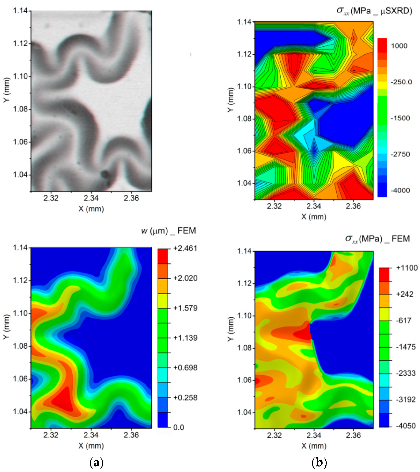
Figure 6. Buckles are scanned using a 10–15 μm step size. For the W film corresponding to region III in
Figure 1, the comparison of the in-plane geometries between the optical image and the FEM simulation is shown in
Figure 4a. The results show a good agreement between the numerical and experimental methods. In
Figure 4b, the X-ray measured stress map shows that the stress in the adherent film outside the delaminated region is about −4000 MPa and reaches about +1000 MPa at the top of the buckling. In the simulation, we observed the same trend when choosing the value of equi-biaxial residual stress in the adhesive region to be about −4000 MPa, which leads to a value of +1100 MPa at the top of the buckling. The existence of huge compressive stresses in W films is mainly due to the deposition process (ion beam sputtering). Indeed, the deposited atom energy is relatively high (between 100 and 1000 eV) which leads to the well-known “atomic peening” effect [
32]. A large number of defects are produced in the crystallographic lattice (self-interstitials, for instance) leading to strong distortions which can be revealed by an increase of the stress-free lattice parameter with respect to the reference value. In addition, the grain sizes are nanometric, considerably influencing the yield stress of W (value increase compared to coarse grain value), and thus could explain the presence of such large residual stresses in the film. Furthermore, the geometry of the system thin film/rigid substrate confers specific mechanical properties to the film.
Figure 5 shows the stress map obtained by FEM calculation compared to the output of a μSXRD scan performed over a circular blister with a diameter of 54 μm in a 630-nm-thick Au film on Si. The stress map obtained by μSXRD shows that the stress in the adherent film in the vicinity of the blister is about -400 MPa while it vanishes to around 0 MPa in the middle of it. The FEM stresses vary from −400 MPa to +21 MPa. For Au films, the stress amplitude in the adherent part is slightly less than the yield stress value (500 MPa) observed in the literature for such films, i.e., same order of grain sizes [
33]. Plasticity certainly occurs at the edge of the blister [
34].
Figure 6b shows the stress map over an isolated telephone-cord wrinkle in the W film. The biaxial stress in the adherent region is about −6000 MPa while it reaches a value of about +1000 MPa at the top of the wrinkles in μSXRD experiment; the FEM stresses vary from −6000 MPa to +949 MPa in
Figure 6b.
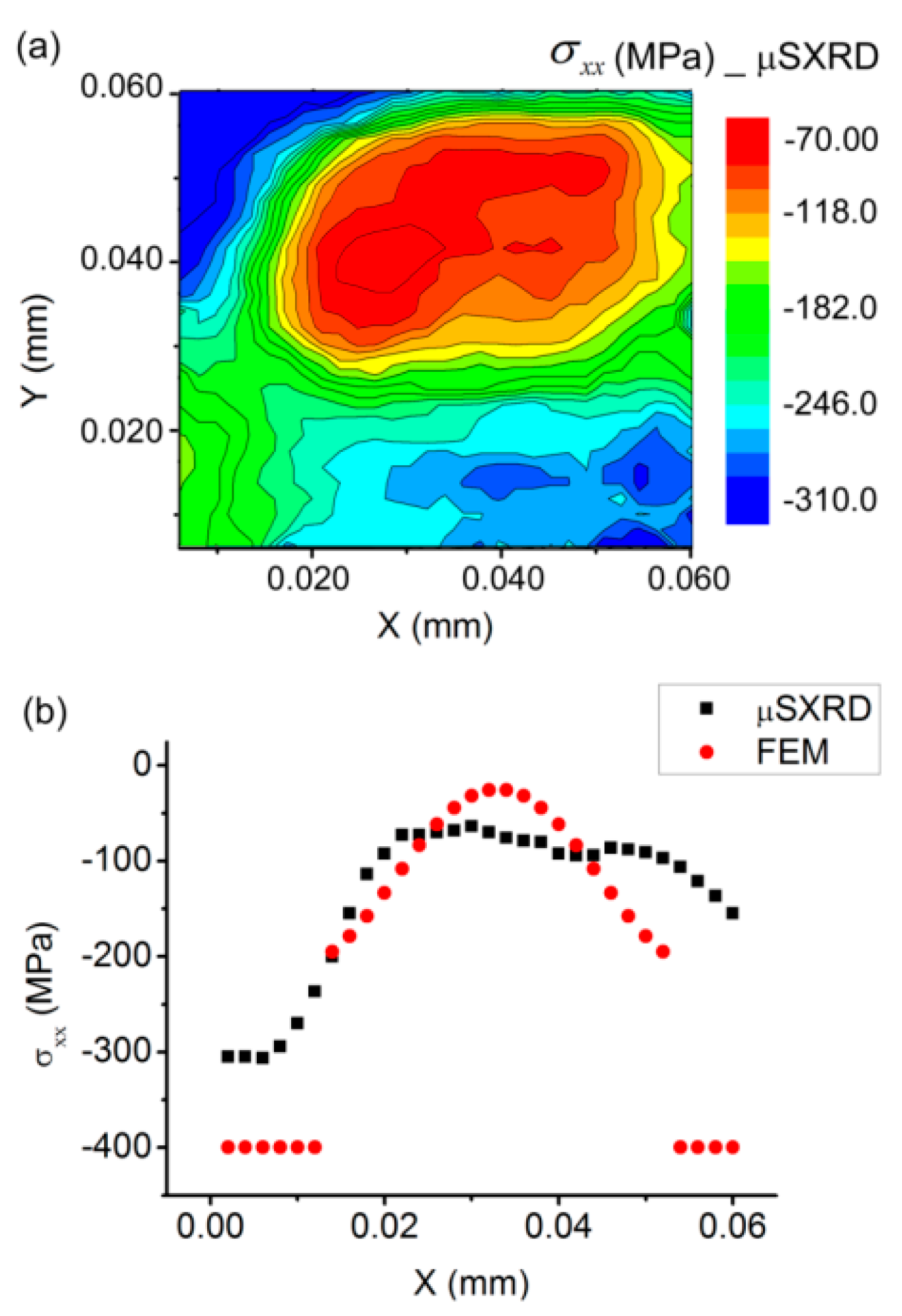
The output of a μSXRD scan performed over a circular blister (diameter = 40 μm) of a 630-nm-thick Au film on Si is shown in
Figure 7a. The scan was performed with a 2-μm step size using 300 s exposure time at each step for diffraction pattern recording. The stress map shows that the stress in the adherent film in the vicinity of the blister is about −400 MPa while it vanishes to around 0 MPa in the middle of it. The stress profiles across the blister in the experimental and FEM results are in overall good agreement (
Figure 7b). The transition is sharp for finite element modeling (see the explanation below) while it is smoothed for X-rays. The effect in this last case is explained by the beam size, which is almost twice the step size.
In these four buckling examples, a very good agreement is found between FEM and μSXRD stress maps since the minimum and maximum of stresses appear almost at the same locations with the same amplitude for both methods. The main difference between W and Au materials is that plastic damage occurs in the latter at the edges, i.e., the circumference of the buckle. Another difference is related to stress release since the stress is almost 0 at the top for Au blisters while it is in tension (positive stress) for W. Let us remember that there exists an in-depth stress gradient through the film thickness in the buckling region. This is not taken into account in our comparison since μSXRD only provides an average value through the film thickness.
In the FEM calculation, the bonded films outside the buckling regions are considered as constrained by the stiff substrates. As a result, the stresses are just released in the buckling region while the levels of the initial residual stresses remain constant in the bonded region. Therefore, a break of the stress distribution is presented at the buckling edges. This indicates that the stresses are released suddenly from the bonded film to the wrinkles and blisters in our FEM results. This may be improved by introducing the adhesion model at the interface between the film and the substrate [
5,
35].
The precision for μSXRD stress mapping could be improved by taking into account the variation of the normal to the sample surface adding a correction to the “
d vs. sin
2Ψ” plot during the buckling scan [
36]. For instance, a maximum deviation of 12° may be expected for an Au blister with a width of 40 μm, see
Figure 7. This effect could be corrected if the coordinates of the normal to the blister are known. This could be done by applying atomic force microscopy in tapping mode [
37]. Otherwise, the value of the angular position of the maximum intensity in the diffraction ring is well known and does not change during the buckling scan. An extension of the Ψ-angular domain of measurement would also greatly increase the precision of stress determination. On the other hand, the surface curvature does not affect the precision of stress measurement; for instance, the radius of surface curvature in Au film blisters (135 microns) is much larger than the X-ray spot size (µm
2) [
38]. Moreover, μSXRD is not suitable for the dynamic measurement of the delaminating process, such as the propagation of telephone-cord and straight-sided buckling [
5,
39].
6. Conclusions
Studies on thin film buckling on stiff substrates by micro-scanning X-ray diffraction (μSXRD) and finite element method have shown that the stresses are released when the film buckled away from the substrate. μSXRD experimental results on Au and W films after deposition have been presented. It is confirmed that μSXRD is able to investigate the stress distribution of film buckling at the micron scale. This leads directly to accurate stress maps of the investigated wrinkles and blisters.
Buckling geometry can be extracted from optical measurements and then introduced into the finite element model to simulate the buckling behavior. Very accurate values at the edges of the delamination geometry are directly measured from optical images and especially for complex wrinkles such as those obtained for W films. This information is of great interest since the nonlinear calculation of instability of the thin film model in FEM has been performed taking into account the measured residual stress and the geometric parameters extracted from optical measurements. With such an approach, we can easily model complex wrinkles since the propagation of the crack occurring at film/substrate interface is ignored. However, sharp variations of stresses at edges are not realistic. This problem could be improved by taking into account film adhesion to the substrate and interface sliding.
Microdiffraction measurements can be improved further for quantitative comparison with FEM stress maps. First, the spatial resolution used in this study is too large with respect to the buckling dimensions. X-ray beam size of less than one micron for such polycrystalline films with nanometric grain sizes would be adequate. Second, the total stress tensor is needed since FEM allows the calculation of all components.


