Article

Blue Diode Laser Welding of Commercially Pure Titanium Foils

1
Department of Mechanical and Manufacturing Engineering and Technology, Oregon Institute of Technology, Klamath Falls, OR 97601, USA
2
AIM-HI, National Chung Cheng University, No. 168, Section 1, Daxue Rd, Minxiong Township Chiayi County 62102, Taiwan
3
Loewy Institute, Department of Materials Science and Engineering, Lehigh University, Bethlehem, PA 18015, USA
4
Joining and Welding Research Institute (JWRI), Osaka University, Osaka 567-0047, Japan
5
Department of Mechanical Engineering, Auckland University of Technology, Auckland 1010, New Zealand
6
Department of Mechanical Engineering, Universitas Jember, Jember 68121, Jawa Timur, Indonesia
*
Author to whom correspondence should be addressed.
Quantum Beam Sci. 2022, 6(3), 24; https://doi.org/10.3390/qubs6030024
Submission received: 26 February 2022 / Revised: 1 July 2022 / Accepted: 12 July 2022 / Published: 18 July 2022
(This article belongs to the Special Issue Laser Assisted Manufacturing)

Abstract

:
The need for thin foil welding is increasing significantly, particularly in the electronic industries. The technologies that are currently available limit the joining processes in terms of materials and their geometries. In this paper, a series of trials of fusion welding (bead-on- plate) of commercially pure titanium (CPTi) foils were conducted using a blue diode laser (BDL) welding method. The power used was 50 W and 100 W for 0.1 mm and 0.2 mm thick foils, respectively. Following welding, various samples were prepared to examine the weld profiles, microstructures, hardness, tensile strength, and fracture surface characteristics. The results showed that the base metal (BM) had an annealed microstructure with equiaxed grains, while the weld zones contained martensite (α’) with large grains. The hardness increased in both regions, from around 123 HV to around 250 HV, in the heat-affected zone (HAZ) and fusion zone (FZ) areas. The tensile tests revealed that the strengths of the welded samples were slightly lower than the unwelded samples, i.e., UTS = 300–350 MPa compared with 325–390 MPa for the unwelded samples. Fracture took place within the BM area. All of the samples, welded and unwelded, showed identical fracture mechanisms, i.e., microvoid coalescence or ductile fracture. The weld zone experienced very small strains (elongation) at fracture, which indicates a good weld quality.

1. Introduction

The blue diode laser (BDL) is one of the laser technologies that is commonly used in applications such as lights for projectors and general lighting. However, many more potential applications are possible in the near future if the laser’s power and brightness can be increased [1,2]. A new generation of blue diode laser (BDL) has recently been developed at the Joining and Welding Research Institute (JWRI), Osaka University, in collaboration with Shimadzu Corporation, Japan. The welding machine has a power of up to 100 W and an energy density of 1.3 × 10⁶ W/cm2 at the end of the output fiber. This new device uses a GaN-based diode [1] and is expected to be used as a light source for various applications, including welding of the so-called difficult-to-weld metals such as gold, copper, and other reflective metals as well as in 3D printing of such metals because blue light can be efficiently absorbed by these metals [1,2]. Given its very small spot beam size, BDL technology can also be applied extensively to thin foil manufacturing, such as in cutting and/or welding processes. Joining (welding) of thin foils has always been required, for example, in battery cell applications [3]. In addition, with a very small spot size, the heat distortion is also minimized, which means post-weld heat treatment to remove residual stresses may not be required [1]. Furthermore, it is also expected to contribute to reducing the processing time and electrical power consumption in these applications, which is not possible with conventional modules. More details about the BDL machine developed at the JWRI can be found in the paper by Tojo et al. [1].
The need for thin foil welding is increasing significantly, particularly in electronic industries. The technologies that are currently available are limiting the joining processes in terms of materials and their geometries. Several welding experiments on thin foils have been reported where the infra-red or direct laser was utilized, but none have reported on titanium foils. Ventrella and co-authors [4] used infra-red laser technology to weld 0.1 mm thick stainless steel 316 L foils. Following the experimental work and analyses, they concluded that the quality of the thin foil weld was good in terms of the mechanical properties. Abe et al. [5] utilized a direct diode laser to weld 0.05 mm SS304 stainless steel without any spatter and reported a nearly equal strength as the un-welded samples. Kim [6] reported their findings following welding of a 0.05 mm thick AM350 stainless steel foil onto SS304 stainless steel with a thickness of 1 mm. They concluded that the beam diameter played a significant role in thin foil welding, and further recommended that a smaller beam diameter would be preferred. Pakmanesh et al. [7] performed a lap joint of a 316 L stainless steel foil using a pulsed Nd:YAG laser to optimize the process parameters. It was concluded that the underfill and undercut increased with the increased power. On the one hand, the underfill increased with a reduced frequency; however, on the other hand, the undercut increased with an increased high frequency. The authors managed to overcome the presence of these defects by superimposing different responses. The above-mentioned welding methods are, however, not suitable for bright and reflective metals such as copper, and gold; therefore, the development of new technology is still needed.
Limited articles have been published on blue laser or blue diode lasers related to welding, cladding, and materials processing, and they are summarized in the following. Das et al. [3] performed welding of multi-layered stainless steel (SS316L) by stacking 20 layers of micro-foils with a thickness of 0.025 mm onto a 0.2 mm thick SS316L foil sandwich and welded them together. They suggested that this welding technique is suitable for industrial needs, especially for electrical micro joining, as it results in free cracks, low porosity, and low spatter. Zediker et al., conducted welding on copper using a blue laser with a power of 500 W and a spot size of 215 µm. They were able to perform welding at an angle of 90°. The authors reported that neither porosity nor spatter was found [8]. In addition, Zediker et al., performed a full penetration bead-on-plate welding on copper with a power of 600 W and a spot size diameter of 200 µm. They concluded that the shorter wavelength, such as that of the blue laser, is well absorbed by copper [9]. Wang et al., used a blue diode laser of 250 W for material processing for successful laser irradiation on a steel sample [10]. Suwa et al., developed a blue laser for processing copper foils and melting copper powder, with a power of 100 W and a core diameter of 100 µm. The blue laser is called BLUE IMPACT, and they stated this new laser technology can improve the manufacturing quality of copper for electronic and automotive applications [11]. Another blue laser that was recently developed was reported by Konning et al., at Coherent DILAS. The authors reported two types of modules, both with a wavelength of 450 nm—one module with 500 W power and a 200 µm core diameter, and the second with 550 W power with a 400 µm core fiber. The intention of this newly developed laser technology was for material processing [12]. The BDL technology at JWRI has been successfully used for cladding pure copper on a stainless steel (SS304) substrate [13,14]. Hummel et al. [15] conducted a feasibility study by conducting micro-welding of copper using a diode laser with a wavelength of 450 nm (no other detail was provided, but presumably a BDL) and 150 W of power. The thickness of the copper samples ranged from 150 µm to 1 mm. It was concluded that the butt and lap joints could be satisfactorily achieved up to a thickness of 500 µm with a speed of up to 10 mm/s. Xu et al. [16] compared the cladding characteristics of copper on martensitic stainless steels using TIG and diode laser methods. They found out the laser cladding had fine microstructures, a narrow heat-affected zone, and excellent wear resistance compared with the TIG method. Separately, Boese et al. [17] reviewed blue laser technology with added power and brightness, and suggested that this technology allowed for welding copper samples and that it also improved the ability to weld dissimilar metals, for example, copper to stainless steels or copper to aluminum alloys.
In this paper, the results from the recent investigation on the welding of CP Ti foils using the BDL welding method are presented. The purpose of this work was to establish if BDL could be applied to the welding of thinner metallic foils and higher welding speeds. At this stage, the focus of the work was on relatively less-bright metals such as titanium to identify the possible parameters for the subsequent welding of the thin copper or gold foils. The microstructure and the strength of the welds were examined. In addition to the hardness and tensile testing results, a digital image correlation (DIC)—a post-processing feature following the tensile testing—was also conducted to gain a better understanding of the weld response to tensile stresses. The fracture surfaces from the tensile testing were also examined with the scanning electron microscope (SEM) and are reported in this paper.

2. Experimental Procedures

2.1. Materials

The material used in this investigation was commercially pure titanium (CP Ti) Grade 2 foil with a thickness of 100 µm and 200 µm. The nominal composition of the material is given in Table 1.

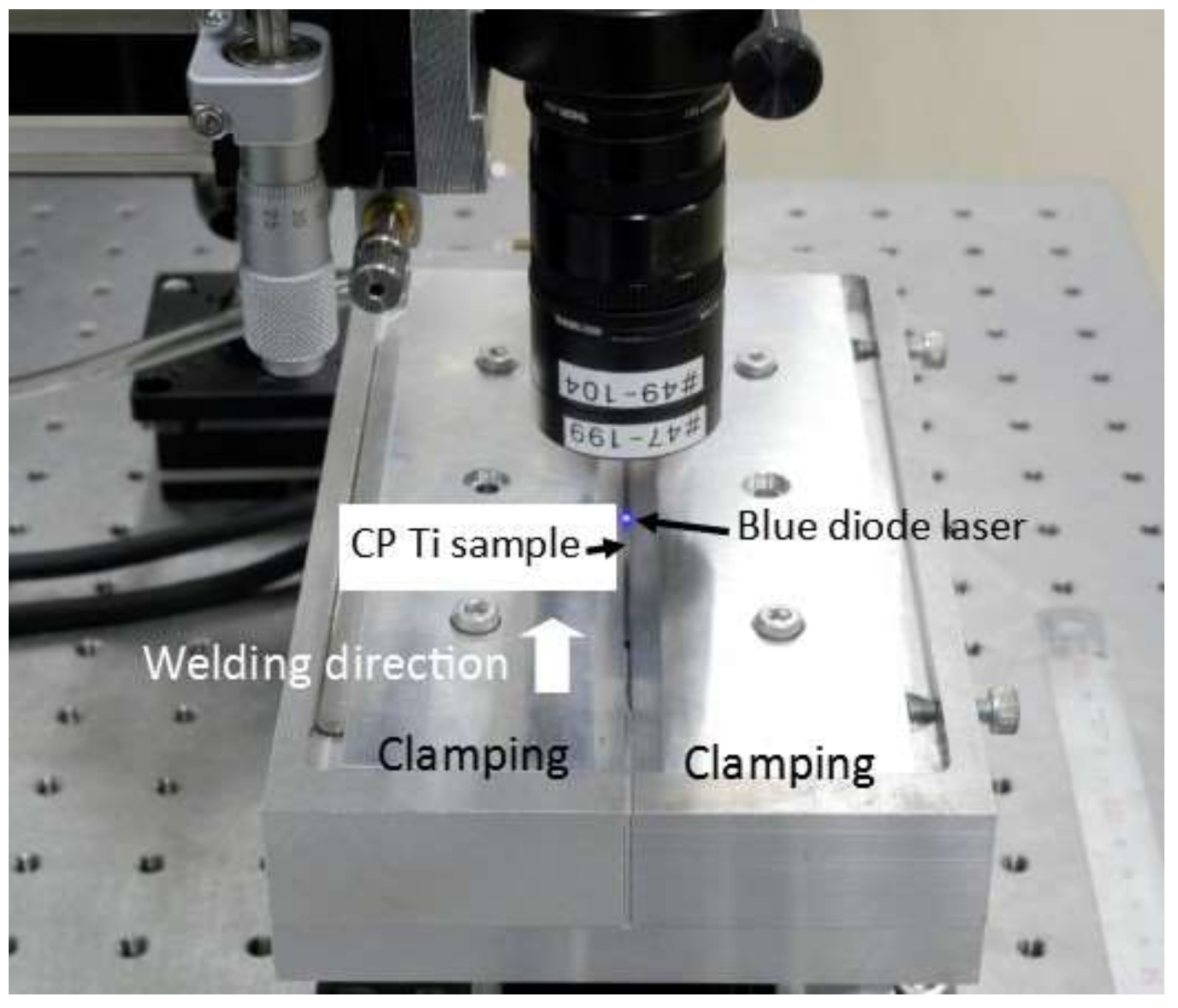
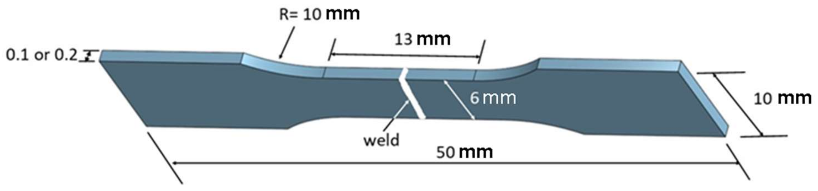
2.2. Welding Procedures

Bead-on-plate using a blue diode laser welding technique was performed at the Joining and Welding Research Institute (JWRI), Osaka University, Japan. Prior to welding, the foils were cleaned thoroughly with ethanol to ensure they were free from dirt, grease, and other surface contaminations. The system employed up to six diode laser modules with a single module power of around 20 W. The focal spot of the laser light had a top-hat profile of 100 µm diameter. The welding was performed without any filler metal (autogenous) with the following parameters: 50 and 100 W of power and a welding speed of 20 and 30 mm/s for the 100 µm and 200 µm thick foils, respectively, and a wavelength of 450 nm. Note that the speed used in this investigation was 2–3 times higher than what was reported previously [9]. Pure argon gas (purity of up to 99.9%) was used as shielding with a flow of 25 L/min. The welding heat input was estimated to be between 1 and 5 J/mm.
The schematic diagram of the BDL welding used in this investigation is given in Figure 1. More details about the BDL system at JWRI have been provided by Sato et al. [13] and Asano et al. [14].

2.3. Metallography

For the microstructural and microhardness examinations, metallographic samples were prepared from the welded specimens. The samples were cut in the normal to the welding direction. They were mounted in a conductive bakelite resin. The mounted samples were ground using SiC paper up to 2400 grit size and were polished down to 0.05 µm using colloidal silica on polishing cloths. The polished samples were etched with Kroll’s reagent (100 mL H2O + 2 mL HF + 5 mL HNO3) and were examined using an Olympus BX51M optical microscope to characterize the microstructures.

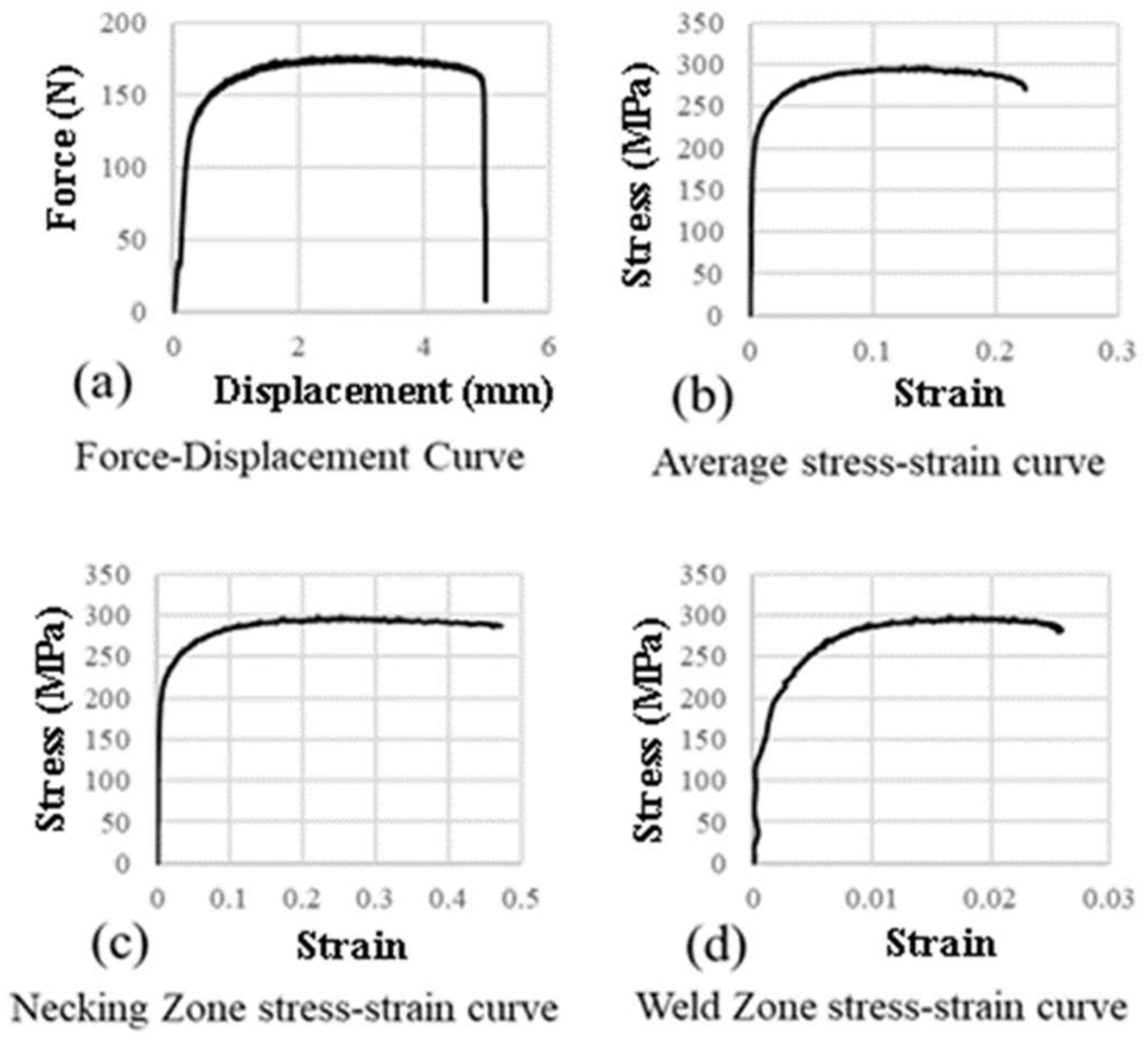
2.4. Mechanical Testing

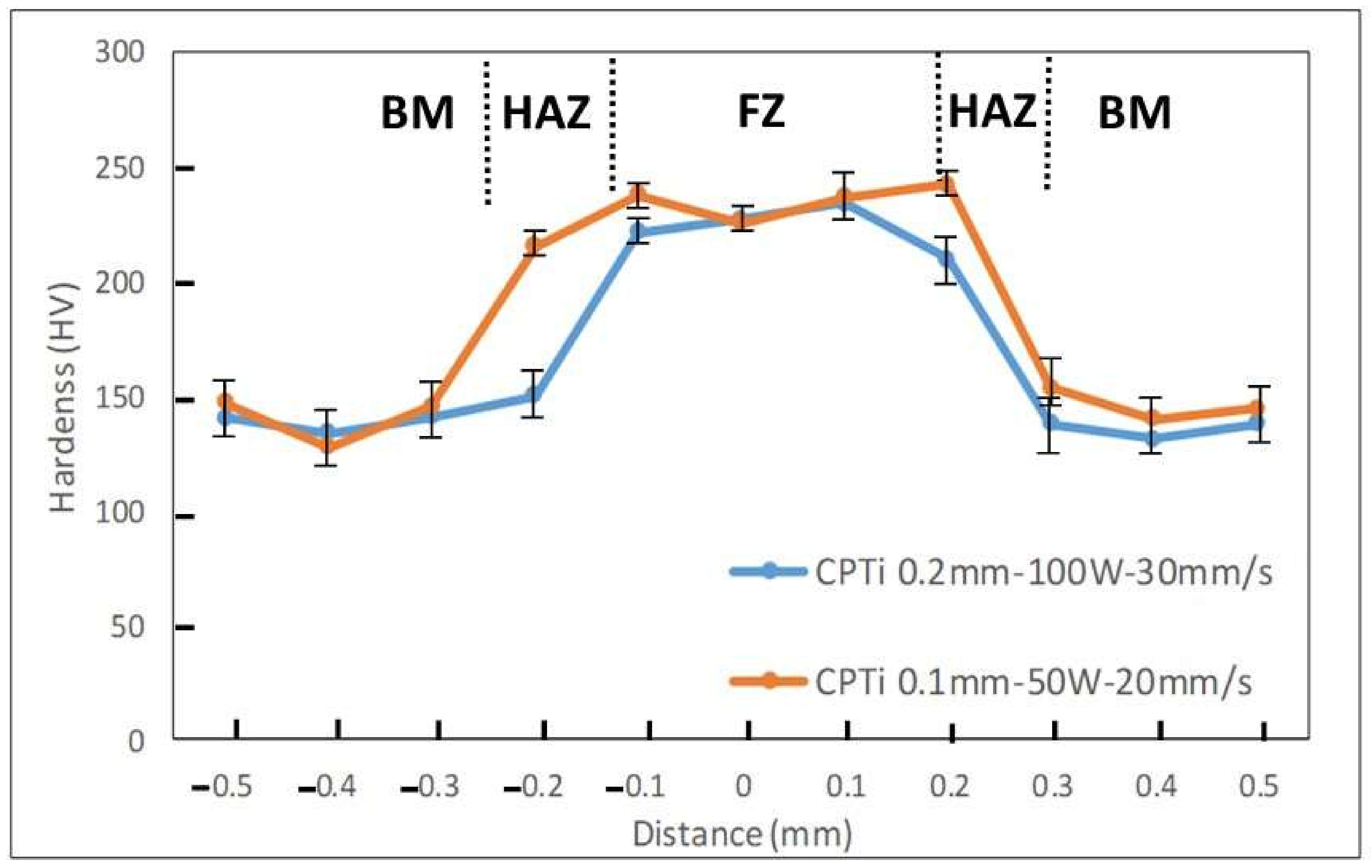
2.4.1. Microhardness

To produce the hardness profiles, micro-hardness tests were conducted on the polished and etched samples using a Vickers machine (Leco AMH 55, St. Joseph, MI, USA) with a load of 50 g and a dwell time of 10 s. Indentations were made on the base metal (BM), heat-affected zone (HAZ), and the fusion zone (FZ). The results were then plotted to determine the hardness profiles.

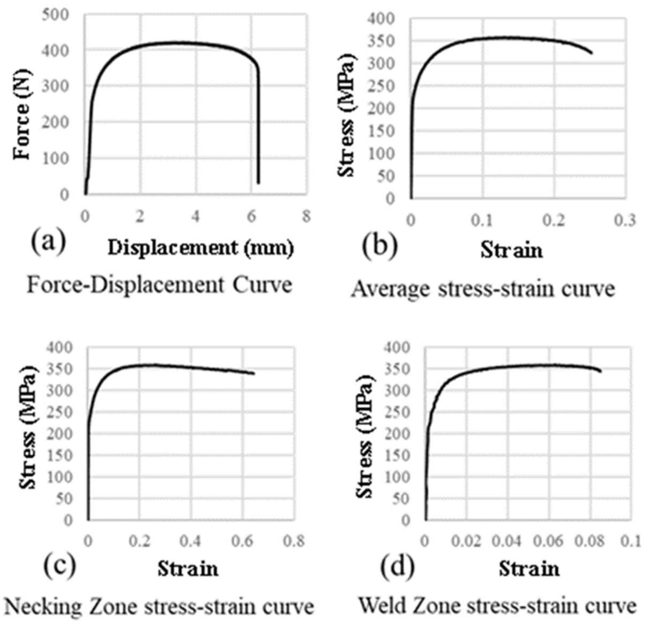
2.4.2. Tensile Testing

Tensile testing was conducted on dog bone-shaped samples using the Shimadzu Universal Testing Machine model AG-IS (Shimadzu, Kyoto, Japan) with a crosshead speed of 0.07 mm/s. Three samples were tested for each welding condition. The dimensions of the samples are shown in Figure 2. The tensile testing machine used was equipped with a digital image correlation (DIC) system with a couple of 5.0 Megapixel CCD cameras. This non-contact technique was employed to measure the overall strain, its distribution, and the local strain gradients at the fracture locations. The post-processing of the DIC was performed and analyzed using the VIC-3D system (Correlated Solutions, Irmo, SC 29063, USA).

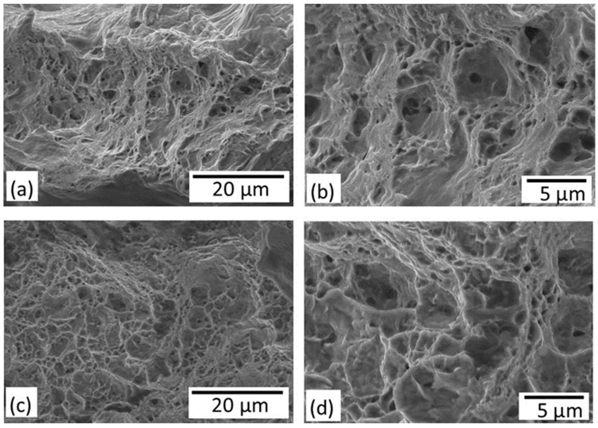
2.4.3. Fracture Surface Examination

A scanning electron microscope (SEM), Hitachi SU70 (Hitachi High-Technologies Corporation, Minato-ku, Tokyo, Japan), was employed to study the fracture surfaces following tensile testing. The samples were prepared using ultrasonic cleaning for 10 min using ethanol prior to the SEM examinations.

3. Results and Discussions

The general appearance of the CP Ti foils with weldments are shown in Figure 3.
A full penetration bead-on-plate was achieved for both foils (Figure 3 and Figure 4) with the parameters indicated in Section 2.2. The weldments showed a V-shaped configuration for the FZ and HAZ zones (Figure 4). The width of the weldments was up to 450 µm and 200 µm on the face and the root surfaces for the 100 µm thick foil, and up to 700 µm and 250 µm for the 200 µm thick foil for the face and root surfaces, respectively. It is also worth mentioning that there was very little distortion during metallography handling of the weldments. The slight bend of the 0.1 mm sample (Figure 4a) might be due to the handling of the sample after welding or during the metallography sample preparation.
The microstructure of the base metal showed an annealed structure with equiaxed grains (Figure 4). They were approximately between 5 and 10 µm in diameter. In the FZ area, the grains were fairly large, i.e., up to 20 µm in width and 100 µm in length. The grain size in the HAZ was smaller than for the grains in the FZ, but larger than in the BM area. A few cases of twin grains were also observed within the base metal and the weld zones. It was also noted that the weld zones, particularly in FZ (Figure 5), contained the α’ structure (martensite), which is the main strengthening element in titanium alloys, including the high-grade CP Ti used in this investigation [18,19,20,21,22,23,24,25]. In addition, lamellar α phases were also present in the weld zone, especially in the FZ area [18,23,24]. More detailed information regarding the microstructures of CP Ti welds can be found in Danielson et al. [18] and Lathabai et al. [22].
The results from the microhardness testing showed that HAZ and FZ had higher hardness compared with the base metal (Figure 6 and Figure 7). This probably is due to the presence of α’ (martensite) in WZ. The presence of α’ is associated with a fast cooling rate because both samples were fairly thin. Danielson et at. reported an increase in the weld zone area due to a high oxygen content [18]. In addition, the hardness of the 100 µm thick foil on the HAZ area increased earlier than that of the 200 µm thick foil due to its thinner size; hence, it had arguably faster cooling rates and more martensite (α’) compared with the later foil.
The tensile testing results are presented in Table 2. The results from the DIC analysis are presented in Figure 8, Figure 9, Figure 10 and Figure 11.
Figure 8 and Figure 9 show the strains within the samples at various location along the gauge length for the 100 µm and 200 µm thick foils, respectively. At an early stage, e.g., roughly less than 5% strain (Figure 8b and Figure 9b), it is obvious that localized strains (necking) started to take place on each side (outside) of the weld zone, as indicated by the red color. Necking continued within these areas until the strains reached around 15 to 17% before a localized necking at a “single” location prior to fracture (Figure 8d and Figure 9d). Figure 8d and Figure 9d present the strain experienced by the samples upon fracture, i.e., around 22% and 25% for the 100 µm and 200 µm thick samples, respectively. The reason for the slightly higher percentage of strain (i.e., higher elongation) on the 200 µm thick samples could be due to their thicker sizes, which may delay the localized strain taking place. All of the tested samples fractured outside the weldments, which indicated a good weld quality and strong joints (also shown and confirmed by the high hardness in the weld zones).
Following the tensile testing, the DIC results were post-processed, and various relationships were derived including force vs. displacement, stress vs. strain, stress vs. strain at the necking zone, and stress vs. strain at the weld zone (Figure 10 and Figure 11). These diagrams provide detailed information about the loads, displacements, stresses, and strains across the gauge lengths, weld zones, and fracture locations. The maximum forces recorded during the tensile testing were around 180 N for the 100 µm thick foil and around 420 N for the 200 µm thick foil. The displacements of the samples were found to be around 5 mm and 6.2 mm for the 100 µm and 200 µm thick foils, respectively. The unwelded foil samples had higher strengths (UTS) and elongations than the welded samples, which was, arguably, due to the uniform stress and strain distribution along the entire sample’s gauge length. Additionally, the unwelded foil samples presented uniform strength distribution within the entire gauge, resulting in one localized deformation site (necking). For the welded samples, the presence of weldment (shown by the fine weld line) in the middle of the gauge length limited the stress and strain distribution to a much more limited volume in the test sample. In other words, the much smaller actual gauge size is found on each side of the weldment. Hence, relatively the early fracture resulted in slightly lower strengths and elongations compared with the unwelded samples. More detailed information about the strengths (both the yield and ultimate tensile strengths) can be seen in Table 2.
The strains deduced from the DIC system are presented in Figure 10b–d and Figure 11b–d. The average strains (measured on the whole gauge length) showed 0.22 (22%) and 0.25 (25%) for the 100 µm and 200 µm thick samples, respectively. Within the necking zone, the 100 µm thick samples experienced a 0.46 (46%) strain compared with the 0.61 (61%) strain on the 200 µm thick samples. The DIC may also provide strains specifically in the weld zone area. The strain within the 100 µm thick samples was around 0.026 (2.6%), while the 200 µm thick sample had a strain of around 0.085 (8.5%). The weld zones area clearly did not experience significant strains compared with the other areas of the samples, which indicates a good weld quality (weld defects, if any, were not detected) and strong joints.
As indicated in Table 2, fractures for all of the welded samples occurred at the base metal (BM) locations. The examination of the fracture surfaces using scanning electron microscopy (SEM) showed a relatively highly ductile behavior with the presence of dimples throughout the surfaces (Figure 12). No indication of weld defects, such as porosity, gas bubbles, or lack of penetration, was observed. The presence of dimples on the fracture surface indicated a micro-void coalescence mechanism present for both specimen thicknesses.

4. Summary

Based on the performed investigation, the following can be concluded:
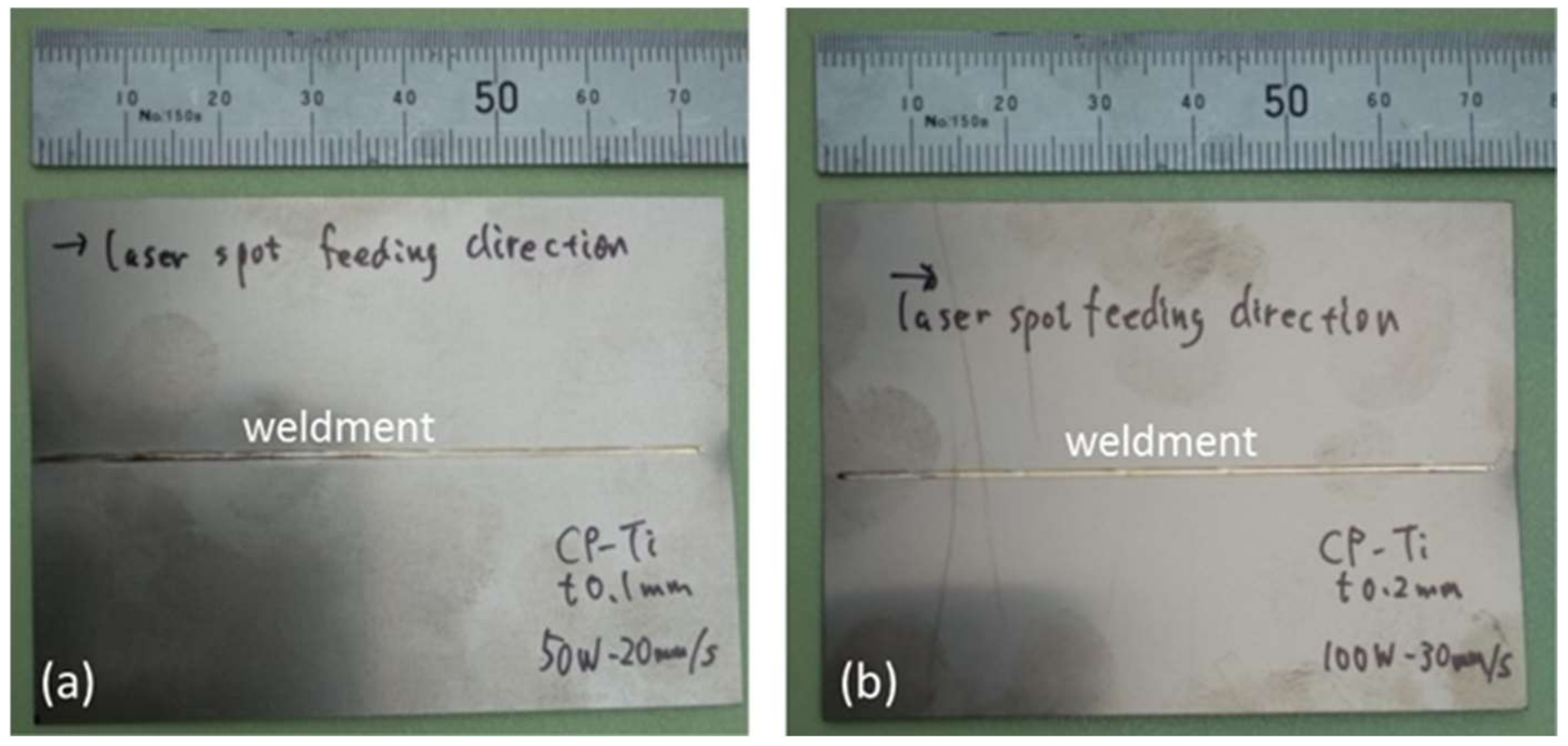
  • The blue diode laser (BDL) can be successfully used to perform welding on thin metallic foils such as CP Ti with thicknesses of 100 µm and 200 µm, and with a speed of up to 30 mm/s.
  • Although the samples were fairly thin, there was no distortion observed on the welded samples associated with the BDL process.
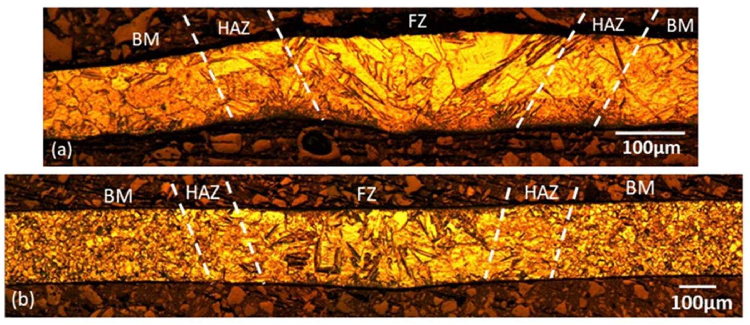
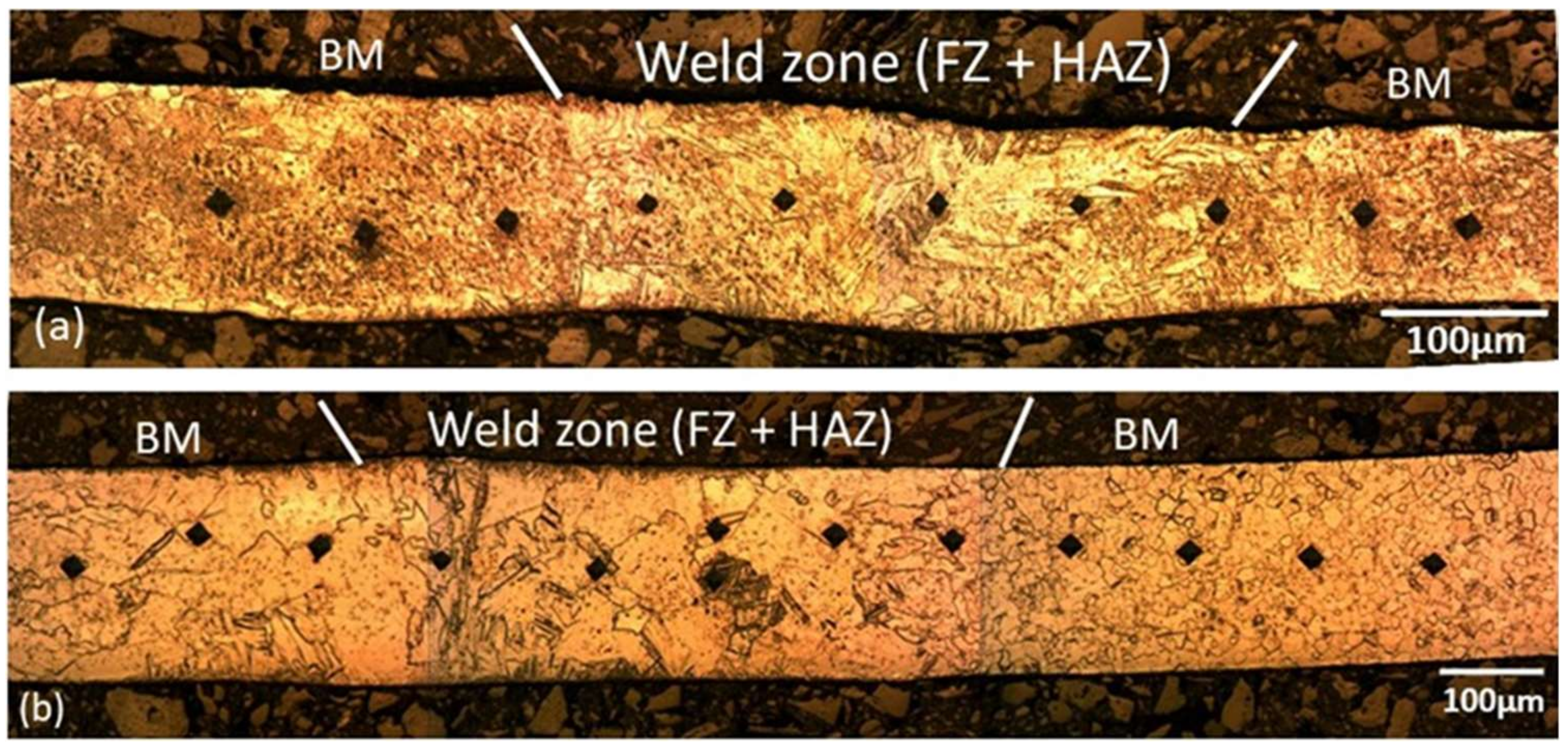
  • The weld zone (FZ and HAZ) displayed a high hardness (strengths) compared with the base metal (BM). This is due to the formation of α’ (martensite) within the HAZ and FZ.
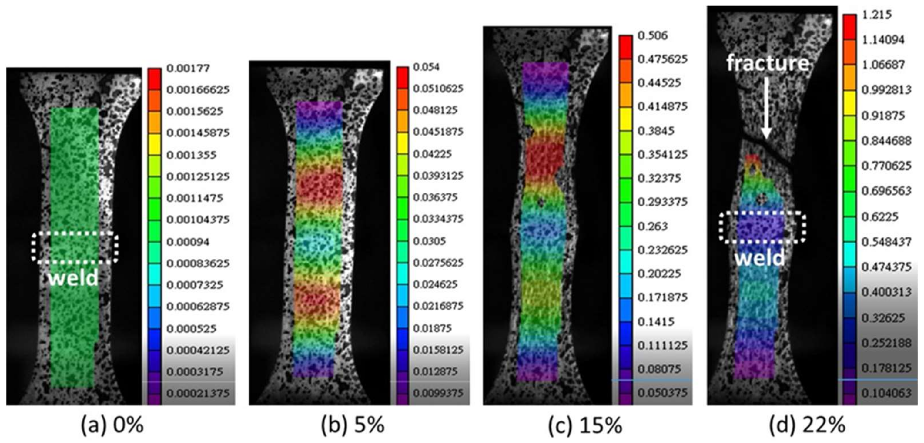
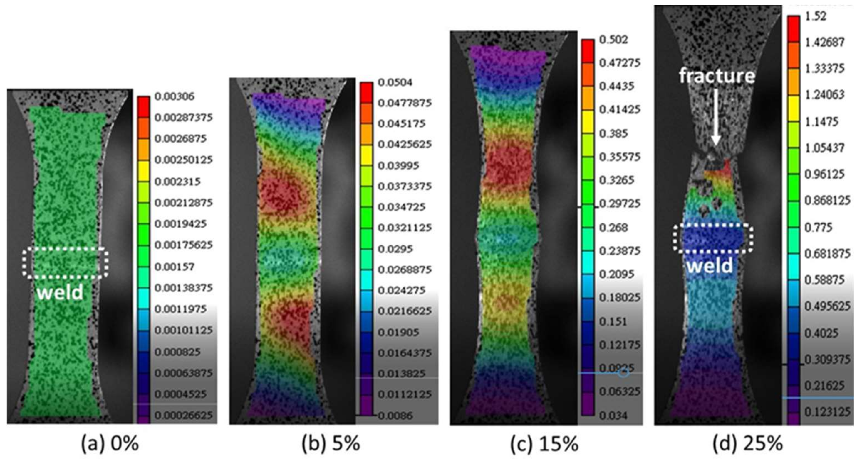
  • Based on the DIC results, the strains observed were concentrated within the BM where the fracture eventually took place. The samples fractured with a microvoid coalescence (ductile) mechanism where dimples can be observed throughout the fracture surfaces. This implies good weld quality and strong weld joints.

Author Contributions

Conceptualization, T.P.; methodology, experiments, writing—draft preparation, and editing, P.-C.L.; experiments and analysis, W.Z.M.; analysis and editing, J.-Y.W.; experiments and visualization, S.M.; experiments, M.T., supervision and funding acquisition, E.H.; experiments and investigation, Y.S.; investigation and supervision, Y.T.; experiments and analysis, D.Y., experiments and data curation, S.Y., experiments and data analysis. All authors have read and agreed to the published version of the manuscript.

Funding

This research was funded by JWRI, Osaka University, UNDER, JIJRec, 2019.

Acknowledgments

The work on the blue diode laser (BDL) has been promoted by the New Energy and Industrial Technology Development Organization (NEDO) project under “Development of advanced laser processing with intelligence based on high-brightness and high-efficiency laser technologies (2016–2020)” project. One of the authors (T.P.) would like to thank JWRI for its generous support under the JIJRec scheme in order to be able to carry out the experiments at JWRI, Osaka University. In addition, two co-authors (T.P. and W.Z.M.) would also like to thank the Lowey Institute at Lehigh for their continued support up until the completion of this manuscript.

Conflicts of Interest

The authors declare no conflict of interest.

References

  1. Tojo, K.; Masuno, S.; Higashino, R.; Tsukamoto, M. Project Works towards Goal of Next-Generation Laser Processing System with High-Power Blue Diode Lasers. Available online: https://www.industrial-lasers.com/cutting/article/16485172/japan-develops-blue-laser-for-advanced-materials-processing (accessed on 1 September 2018).
  2. Nakamura, S.; Pearton, S.; Fasol, G. The Blue Laser Diode: The Complete Story, 2nd ed.; Springer Science and Business Media: New York, NY, USA, 2000. [Google Scholar]
  3. Das, A.; Fritz, R.; Finuf, M.; Masters, I. Blue laser welding of multi-layered AISI 316L stainless steel micro-foils. Opt. Laser Technol. 2020, 132, 106498. [Google Scholar] [CrossRef]
  4. Ventrella, V.A.; Berretta, J.R.; de Rossi, W. Pulsed Nd: YAG laser seam welding of AISI 316L stainless steel thin foils. J. Mater. Process. Technol. 2010, 210, 1838–1843. [Google Scholar] [CrossRef]
  5. Abe, N.; Funada, Y.; Imanaka, T.; Tsukamoto, M. Micro welding of thin stainless steel foil with a direct diode laser. Trans. JWRI 2005, 34, 19–23. [Google Scholar]
  6. Kim, J.; Kim, S.; Kim, K.; Jung, W.; Youn, D.; Lee, J.; Ki, H. Effect of beam size in laser welding of ultra-thin stainless steel foils. J. Mater. Process. Technol. 2016, 233, 125–134. [Google Scholar] [CrossRef]
  7. Pakmanesh, M.R.; Shamanian, M. Optimization of pulsed laser welding process parameters in order to attain minimum underfill and undercut defects in thin 316L stainless steel foils. Opt. Laser Technol. 2018, 99, 30–38. [Google Scholar] [CrossRef]
  8. Zediker, M.; Fritz, R.; Finuf, M.; Pelaprat, J. Laser welding components for electric vehicles with a high-power blue laser system. J. Laser Appl. 2020, 32, 022038. [Google Scholar] [CrossRef]
  9. Zediker, M.S.; Fritz, R.D.; Finuf, M.J.; Pelaprat, J.M. Stable keyhole welding of 1 mm thick copper with a 600 W blue laser system. J. Laser Appl. 2019, 31, 022404. [Google Scholar] [CrossRef]
  10. Wang, H.; Kawahito, Y.; Yoshida, R.; Nakashima, Y.; Shiokawa, K. Development of a high-power blue laser (445  nm) for material processing. Opt. Lett. 2017, 42, 2251–2254. [Google Scholar] [CrossRef] [PubMed]
  11. Suwa, M.; Wakabayashi, N.; Hiroki, T.; Tojo, K.; Masuno, S.-I.; Higashino, R.; Tsukamoto, M. Development of BLUE IMPACT, a 450nm-wavelength light source for laser processing. In Proceedings of the High-Power Diode Laser Technology XVII, Proc. SPIE 10900, San Francisco, CA, USA, 3–5 February 2019. [Google Scholar] [CrossRef]
  12. Könning, T.; Drovs, S.; Stoiber, M.; König, P.; Kissel, H.; Harth, F.; Köhler, B.; Biesenbach, J.; König, H.; Lell, A.; et al. High brightness fiber coupled diode lasers at 450 nm. In Proceedings of the High-Power Diode Laser Technology XVII, Proc. SPIE 10900, San Francisco, CA, USA, 3–5 February 2019. [Google Scholar] [CrossRef]
  13. Sato, Y.; Tsukamoto, M.; Shobu, T.; Funada, Y.; Yamashita, Y.; Hara, T.; Sengoku, M.; Sakon, Y.; Ohkubo, T.; Yoshida, M.; et al. In situ X-ray observations of pure-copper layer formation with blue direct diode lasers. Appl. Surf. Sci. 2019, 480, 861–867. [Google Scholar] [CrossRef]
  14. Asano, K.; Tsukamoto, M.; Sechi, Y.; Sato, Y.; Masuno, S.-I.; Higashino, R.; Hara, T.; Sengoku, M.; Yoshida, M. Laser metal deposition of pure copper on stainless steel with blue and IR diode lasers. Opt. Laser Technol. 2018, 107, 291–296. [Google Scholar] [CrossRef]
  15. Hummel, M.; Schöler, C.; Häusler, A.; Gillner, A.; Poprawe, R. New approaches on laser micro welding of copper by using a laser beam source with a wavelength of 450 nm. J. Adv. Join. Process. 2020, 1, 100012. [Google Scholar] [CrossRef]
  16. Xu, G.; Kutsuna, M.; Liu, Z.; Yamada, K. Comparison between diode laser and TIG cladding of Co-based alloys on the SUS403 stainless steel. Surf. Coat. Technol. 2006, 201, 1138–1144. [Google Scholar] [CrossRef]
  17. Boese, E.; Finuf, M.; Zediker, M.; Pelaprat, J.M. Blue Lasers Add Power and Brightness. Available online: https://www.industrial-lasers.com/welding/article/14173138/blue-lasers-add-power-and-brightness (accessed on 20 May 2020).
  18. Danielson, P.; Wilson, R.; Alman, D. Microstructure of Titanium Welds. Adv. Mater. Process. 2003, 161, 39–42. [Google Scholar]
  19. Karpagaraj, A.; Shanmugam, N.S.; Sankaranarayanasamy, K. Some studies on mechanical properties and microstructural characterization of automated TIG welding of thin commercially pure titanium sheets. Mater. Sci. Eng. A 2015, 640, 180–189. [Google Scholar] [CrossRef]
  20. Choi, B.H.; Choi, B.K. The effect of welding conditions according to mechanical properties of pure titanium. J. Mater. Process. Technol. 2008, 201, 526–530. [Google Scholar] [CrossRef]
  21. Li, C.; Muneharua, K.; Takao, S.; Kouji, H. Fiber laser-GMA hybrid welding of commercially pure titanium. Mater. Des. 2009, 30, 109–114. [Google Scholar] [CrossRef]
  22. Lathabai, S.; Jarvis, B.L.; Barton, K.J. Comparison of keyhole and conventional gas tungsten arc welds in commercially pure titanium. Mater. Sci. Eng. A 2001, 299, 81–93. [Google Scholar] [CrossRef]
  23. Liu, H.; Nakata, K.; Zhang, J.X.; Yamamoto, N.; Liao, J. Microstructural evolution of fusion zone in laser beam welds of pure titanium. Mater. Charact. 2012, 65, 1–7. [Google Scholar] [CrossRef]
  24. Pasang, T.; Tao, Y.; Azizi, M.; Kamiya, O.; Mizutani, M.; Misiolek, W.Z. Welding of Titanium alloys. MATEC Web Conf. 2017, 123, 1–6. [Google Scholar] [CrossRef] [Green Version]
  25. Lütjering, G.; Williams, J.C. Titanium; Springer: Berlin, Germany, 2007. [Google Scholar]
Figure 1. Blue diode laser (BDL) welding set up.
Qubs 06 00024 g001
Figure 2. Schematic diagram of the dog-bone sample with dimensions (in mm).
Qubs 06 00024 g002
Figure 3. Welded CP Ti foils: (a) 100 µm thick and (b) 200 µm thick.
Qubs 06 00024 g003
Figure 4. Optical micrographs showing weld profiles: (a) 100 µm thick welded with 50 W of power and at a speed of 20 mm/s, and (b) 200 µm thick welded with 100 W of power and at a speed of 30 mm/s.
Qubs 06 00024 g004
Figure 5. High magnification optical micrographs showing the weld centerlines and martensite (α’) phase on the (a) 100 µm thick foil welded with 50 W of power and at a speed 20 mm/s, and the (b) 200 µm thick foil welded with 100 W of power and at a speed of 30 mm/s.
Qubs 06 00024 g005
Figure 6. Hardness indentations on metallographically prepared samples: (a) 100 µm and (b) 200 µm thick foil samples.
Qubs 06 00024 g006
Figure 7. Hardness profiles of the welded samples for two different foils.
Qubs 06 00024 g007
Figure 8. Pictures from digital image correlation (DIC) of CP Ti, 100 µm, 50 W, and 20 mm/s during tensile testing showing sample conditions at various percentages of strain (a) at 0%, (b) 5%, (c) 15%, and (d) 22%, which correspond to fracture. Note: the numbers associated with the images are local strains × 100%.
Qubs 06 00024 g008
Figure 9. Images from the digital image correlation (DIC) of CP Ti, 200 µm, 100 W, and 30 mm/s during tensile testing showing sample conditions at various percentages of strain (a) at 0%, (b) 5%, (c) 15%, and (d) 25%, which correspond to fracture. Note: the numbers associated with the images are local strains × 100%.
Qubs 06 00024 g009
Figure 10. Diagrams showing (a) force−displacement curves and (bd) stress−strain curves representing various stages/places during tensile testing on the 100 µm thick foil, with 50 W of power and at a speed of 20 mm/s.
Qubs 06 00024 g010
Figure 11. Diagrams showing (a) force−displacement curves and (bd) stress−strain curves representing various stages/places during tensile testing on the 200 µm thick foil, with 100 W of power and at a speed of 30 mm/s.
Qubs 06 00024 g011
Figure 12. SEM micrographs showing fracture surfaces of (a,b) 100 µm, 50 W, and 20 mm/s, and (c,d) 200 µm, 100 W, and 30 mm/s.
Qubs 06 00024 g012
Table 1. Chemical composition of commercially pure titanium (CP Ti) in wt.%.
MaterialTiFeHNOC
CP TiBalance<0.3<0.015<0.03<0.25<0.1
Table 2. Tensile data of both the welded (BOP) and unwelded samples.
MaterialThickness (µm)Power (Watt)Welding Speed (mm/s)Yield Strength (MPa)Tensile Strength (MPa)Elongation
(%)
Fracture
Location
CP Ti (BOP)100502014030020BM
14530620BM
14830522BM
CP Ti (BOP)2001003031035523BM
30035025BM
30135025BM
CP Ti unwelded100N/AN/A17032524N/A
200N/AN/A32039028N/A
Publisher’s Note: MDPI stays neutral with regard to jurisdictional claims in published maps and institutional affiliations.

