Time and Frequency Domains Analysis of Chipless RFID Back-Scattered Tag Reflection


Department of Electrical and Computer Engineering, Monash University, Clayton 3800, VIC, Australia
*
Author to whom correspondence should be addressed.
IoT 2020, 1(1), 109-127; https://doi.org/10.3390/iot1010007
Submission received: 23 June 2020
/
Revised: 20 August 2020
/
Accepted: 27 August 2020
/
Published: 8 September 2020
Abstract
:Chipless radio frequency identification (RFID) is a wireless technology that has the potential for many industrial applications, including the internet of things (IoT) applications, in which identification, sensing, and tracking are required. This technology has been improved during the last century. However, the processing of the backscattered signal in a chipless RFID system is still a challenge because the encoded data are embedded in the backscattered signal of a passive tag. The reader hardware, antennas, and the wireless channel have their own response in the received signal, which contains the tag ID information. The tag also produces a response, which is a combination of responses from different resonators, substrate, and copper reflection in a tag. In this paper, the reflection from a typical chipless RFID tag is analyzed, and all components of the backscattered signal are separated in both time and frequency domains. In addition, an equivalent circuit model for a backscattered chipless RFID tag is proposed, and the model is verified based on the actual performance of the resonator. This study has some important implications for future research.
1. Introduction
Nowadays, people’s lifestyles have been changed by the advanced technologies that need identification, tracking, and sensing to build the internet of things (IoT) systems. Radio frequency identification (RFID) is a wireless communication technology for tracking and identification [1], which has a high potential for IoT applications, as discussed in [2]. An RFID system consists of three main components; they are a reader, a tag, and at least one reader antenna. The reader generates a radio frequency signal, transmits it to the tag with the reader antenna, and then measures the reflected signal from the tag. The received signal is processed to extract the tag’s ID. A chipless RFID tag is a passive device devoid of an application-specific integrated circuit (ASIC) chip set. A chipless tag can be printed directly on packaging materials such as paper and plastics. The low-cost chipless RFID tag can make this technology compatible with optical barcodes [3]. However, chipless RFID operates in microwave, ultrawideband (UWB) frequency to extract multiple frequency signatures from the tag as the ID data. As a result, the reader hardware of a chipless RFID system is more complicated than a conventional chipped RFID reader system. This is due to the fact that UWB passive design with octave bandwidth is highly challenging. In addition, there is a significant challenge in encoding data into a passive microwave UWB circuit and extracting the tag’s ID from the backscattered signal. UWB signals have regulatory constraints, hence, they have low transmitted power and, as a result, a weak received signal. The signal processing of the weak backscattered signal is not an easy task.
There are different types of chipless RFID tags, which can be categorized based on their encoding techniques. They are time domain [4,5], frequency domain [6,7,8,9], image-based [10], and the hybrid [11,12] chipless RFID tags. The other type of chipless tags is based on dielectric resonators for encoding data as in [13,14]. Frequency-domain tags are the most prevalent in the open literature in which the data are encoded in the frequency-domain response of the tag. These tags are classified into two groups of co-polar and cross-polar, based on the polarization of the reflected wave from the tag. In a co-polar tag as in [6], the polarization of the transmitted and received wave is the same, while in a cross-polar tag, for example in [15], these waves are perpendicularly polarized.
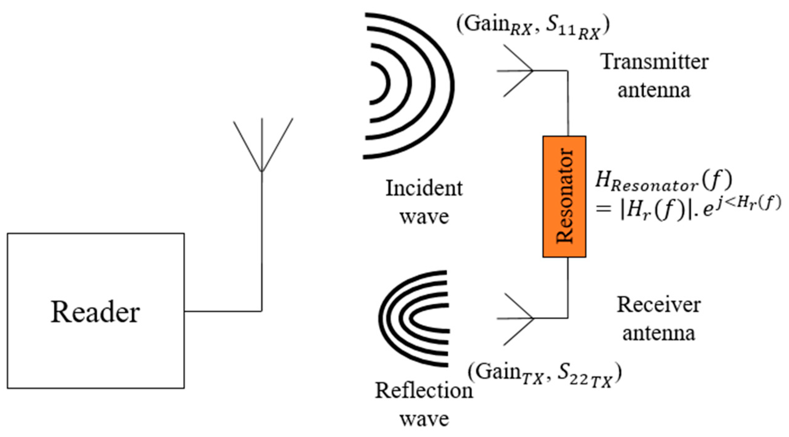
Frequency-domain tags can be a re-transmission type tag, as in [16,17], or a backscattered type tag, as in [11]. A re-transmission type tag consists of one or two tag antennas and a multi-resonator section. The receiver antenna of the tag intercepts the signal transmitted from the reader antenna and passes it to the multi-resonator section of the tag. The resonators generate distinct frequency signatures based on their resonant frequencies and then resubmit the signal through the transmission antenna of the tag. The re-transmitted signal from the tag, due to the multi-resonator circuit, possesses a unique frequency signature, which contains 1:1 correspondence of the tag’s binary ID data. Next, in a back-scattered chipless RFID tag, for example in [18], the antenna is eliminated. The tag consists of multiple resonators, which produce a backscattered signal with a unique frequency signature based on the tag ID. Each resonator receives the UWB incident wave from a reader, modulates the signal with its distinct resonant frequency signature, and backscatters towards the reader (as modeled in Figure 1). Thus, each resonator generates binary ID data with 1:1 correspondence. The frequency signature is with a function of the geometry and size of the resonator, as well as the dielectric constant and thickness of the substrate material of the tag. The resonance/dissonance of the resonator can be seen in the form of a peak, a null, or both peak and null in the UWB frequency response. The multiple resonators with adjacent frequency bands and physical positions have a mutual coupling effect [19]. This may cause frequency shifts of the resonances. In a typical backscattered chipless RFID tag, this coupling effect can also be realized whenever different tag IDs of the tag is generated by shortening or removing corresponding resonators [20,21].
In a chipless RFID system, a reader can process the backscattered signal in time and/or frequency domain [22]. In [23,24], the time and frequency domain response of the tag are investigated. The captured raw data are a combination of multiple components. These components might have an overlap in time and frequency domains and cannot be separated using simple algorithms [25]. Conventionally, in a single-antenna chipless RFID system [26], the return loss of the reader antenna is measured before and after the chipless RFID tag is placed for calibration, which is called background subtraction [27,28]. In this technique, the reflection from antenna and environment is eliminated, but both antenna-mode and structural-mode radar cross-section (RCS) components of the tag are still available with the result.
In [29], a time-gating algorithm to detect a tag ID from a co-polar patch-resonator with delay stubs was proposed to extract the antenna-mode RCS. This technique is limited to the tag detection at ranges longer than 15 cm. Similarly, a short-time Fourier transform (STFT) for depolarized chipless RFID tags detection was proposed in [30], which does not require background subtraction. A depolarized tag [15] has immunity to reflection from the environment; however, two perpendicular polarized antennas are required to detect the tag information. In contrast, a co-polar tag can be detected using only one or two antennas with the same polarizations.
Hence, the mentioned processing approaches are not applicable to a typical backscattered chipless RFID tag that does not produce enough time delays in the desired components, especially in short-range detection scenarios. Also, the estimation of the time arrival of the time window in an inverse problem is another challenge [25]. Although there are some studies on tag response in [22,23,24], there is still a need for further study on the response from a typical co-polar backscattered chipless RFID tag in the short-range detection in order to understand the nature of the generated signal from each resonator of the tag. This study is a preface to move forward to find a solution to extract the desired components of a reflection signal from a typical chipless RFID tag in an inverse scenario.
To mitigate the challenges, this paper analyzes the backscattered signal captured by a single antenna reader system using a typical frequency-domain backscattered tag with 6-bit data capacity. The input return loss (RL) vs. frequency of the reader antenna is modulated with the frequency domain tag signatures and is visible in the RL in dB vs. the frequency plot of the vector network analyzer. A simplified system containing the reader antenna and the tag is simulated in CST Microwave studio suite to collect the required simulated data. Using the generated data from the simulation, different components of the signal, in both time and frequency domains, are extracted and analyzed. The presence of any clutter is avoided in this study. An equivalent circuit model and transfer function for a typical backscattered chipless RFID tag are developed. This model can be customized for any multi-resonator chipless RFID tags. The model is verified by comparing the results with the actual tag performance. In addition, the measured data were also analyzed, and different components were separated. The effect of conventional time-windowing on the measured tag response in short-range detection is also investigated. The investigation states demand for a robust detection technique that mitigates the pertinent challenges, as stated above.
This paper is arranged as follows. Section 2 describes the theory of a chipless RFID system. Section 3 provides the results of different extracted components of the signal in both time and frequency domains, the constructed signal based on the proposed model of the tag, and the measurement results. All the results are also analyzed and discussed in this section. The final section is the conclusion, which provides a summary of the achievements, as well as future projects.
2. Theory
2.1. A Chipless RFID System
The received signal from the reader antenna in a frequency domain chipless RFID system consists of different components: (1) The reflection from the reader antenna, (2) the structural-mode RCS component, (3) the antenna-mode RCS component, (4) reflection from the environment, and (5) noise. All these components have overlapped in both time and frequency domains. The overlap is more significant when the distance between the tag and reader antenna is reduced. Since, in a single antenna reading system, the loading effect of the tag is measured in the form of antenna return loss, the impurity of the reflection coefficient of the antenna is a dominant component in the measured signal.
Secondly, the structural-mode RCS of the tag is generated by the tag physical geometry, including copper and dielectric surfaces of the tag. Ideally, it can be considered as a reflection of the incident signal from the tag with an attenuation and 180 degrees phase shift, in addition to the wireless channel effect. In this case, the component should have a linear behavior regarding frequency, based on the variation of the RCS of the surface. However, due to the shape of the tag and presence of sharp corners on the tag, unwanted scattering centers can be generated, showing up as variations in the frequency signature.
The third component, which is the desired one, is the antenna-mode RCS generated from the tag resonances. Each resonator in the tag produces a frequency signature with a peak and/or null, which can be interpreted as at least one bit of data. The frequency response of each resonator can be distinguished by a frequency shift in the frequency domain response, regardless of the coupling effect between them. On the other hand, the time-domain response of each resonator is different, depending on the characteristic of the resonances. The response of each resonator can have a significant overlap in the time domain, and also, in the received signal, which is a summation of all resonant responses that can be achieved.
Finally, the reflection from the environment and the noise are destructive components in the signal. Depending on the distance of each object in the environment from the reader antenna, the time interval of the reflection from that object varies. The strength of that component depends on the size, shape, and material of the object and its distance to the tag. High reflective objects and high absorptive objects have the most destructive effects. The presence of dielectric objects close to the tag changes the tag frequency signature behavior. This sensitivity to the reflection from the environment and the objects is higher in co-polar tags compared to the cross-polar one [31]. In addition to that, the noise from the reader’s equipment and a dynamic environment are other components of the measured signal, which can be eliminated by noise filtering [32].
Therefore, the total received signal from a tag can be represented by (1).
where is the total signal, and , , , and are the antenna reflection component, the tag structural-mode components, the tag antenna-mode components, and the reflection from the environment, respectively. In addition, when the signal is measured in the absence of the tag, , only the reflection from antenna and environment are present in addition to the noise.
In a conventional background subtraction, the summation of the tag antenna-mode and structural-mode RCS is achieved by a vector subtraction shown in Equation (3)
In theory, in an empty environment, the difference between in two measurements should be zero. This value would be better than −60 dB if the measurement is in an Anechoic chamber limited to the system noise. However, if there is a dynamic noise in the environment or in a non-stationary measurement, this assumption will not be valid.
2.2. Equivalent Circuit Model of a Multi-Resonator Chipless RFID Tag
In this section, the equivalent circuit model of a U-shaped slot tag [33] has been developed. The multi-bit tag consists of six U-slot resonators, which are arranged in a compact size.
2.2.1. Single Resonator Model
In order to study the antenna-mode RCS of the tag, an equivalent circuit model of each resonator is presented in this section. Each resonator can be modeled by an equivalent RLC circuit at the resonance frequency. The voltage source is from the received incident wave to the tag, and the output voltage is the generated voltage/current for producing the reflected wave from the tag. The configuration of the U-shaped slot and the RLC equivalent circuit model of a single resonator are shown in Figure 2a,b, respectively. The resonator has a total length of and a line width of w.
Each resonator can be modeled with a second-order RLC bandpass filter based on the center frequency and the quality factor. By assuming that a typical U-slot resonator (Figure 2a) produces resonance with a center frequency of and a quality factor of Q, its transfer function can be calculated from (4) [34].
where
This transfer function is equal to the transfer function of an RLC bandpass filter (Figure 3a), which can be calculated from (6) [34].
Therefore, by comparing these two equivalent transfer functions, the following can be achieved.
where and are the coefficients of the transfer functions. On the other hand, the inductance of a resonator with a total length of can be calculated by a modification of a cylinder-shaped rectangular loop self-inductance [35].
where can be calculated from (9)
An approximate calculation of the resonance frequency can be found from (10) [36].
As a result, using (6) and inserting the calculated inductance, the equivalent value of the capacitor and resistor can be calculated. Moreover, the time domain transfer function of this bandpass filter will have a formula in the form of multiplication of an exponential with a summation of and functions (11).
where A, B, C, and D are the coefficients that depend on the value of the quality factor and center frequency for each resonator. B has a reverse relation with the time constant of an LC circuit and a function of quality factor and center frequency [37]. is the time delay of each resonance. The exponential coefficient is corresponding to the group delay of each resonance. As a result, the response of each resonance has a rising and a falling envelope.
2.2.2. Multi-Resonator Transfer Function
A chipless RFID tag can be modeled with a two-port network, with a transfer function based on the assumed model depicted in Figure 2b. The transfer function proposed in (4) includes each resonator receiving and re-transmitting antenna return loss, gain, and tag resonance circuit. In a multi-resonator structure, the total transfer function is a summation of individual transfer functions achieved by ignoring the coupling effect between the resonators.
where N is the number of available resonators and is the transfer function of each resonator’s response and can be calculated from (4).
3. Results
3.1. Simulation Results
It is expected that the captured data in the simulation are very close to the real measurement in an Anechoic chamber environment, except the effect of noise in the measured data. So, for this study, most of the processing are based on the simulated system in a CST Microwave Studio suite. The main goal of this study is to understand the nature of different components of a signal in a short-range tag detection.
In order to study the effect of different components in a captured signal in a chipless RFID system, a simplified system was simulated in CST Microwave Studio 2017. The simulation setup of the chipless RFID system is shown in Figure 3 in which the antenna was loaded with a chipless RFID tag. The UWB antenna used in the data generation has an operating bandwidth of 4.4 to 7.8 GHz. The UWB antenna has 9 dBi gain. The 6-bit U-slot chipless RFID tag [26] is designed on Taconic TLX-8 substrate with a thickness of 0.5 mm. The length of each resonator and other parameters of this tag is produced in Table 1. Each slot in this tag generates a resonance in the frequency signature corresponding to one binary data bit of the tag ID. The resonator is defined with bit ‘1’. The short-circuited resonator (filled partially with copper) corresponds to bit ‘0’. Six tags with only one active resonator at different frequencies and one tag with all six active resonators were used for this study.
Firstly, the antenna response was simulated in the absence of any tag for time and frequency domains study. Next, for data generation in simulation, the tag was placed in front of a UWB aperture coupled microstrip patch antenna with a spacing of 5 cm between the tag and antenna. The of the antenna is recorded as the analog output of a chipless RFID system and was processed separately in MATLAB 2018. CST uses an UWB Gaussian pulse as the excitation signal in a time-domain simulator. However, the output of the simulation was the return loss in frequency-domain in two steps of the test, before and after placing the tag for the study. Hence, in order to convert the captured frequency domain S-parameters to a time-domain signal, the return loss of the antenna was multiplied to the UWB Gaussian pulse for further processing. Then, after applying a zero-padding to the frequency domain signal, it was converted to a time-domain signal using an inverse fast Fourier transform (IFFT). This procedure was common for converting each captured S-parameter to a time-domain signal.
The signal is processed by subtracting the time domain antenna effect, , from the capture input signal in the presence of the tag, . The input time-domain signal, , and the processed signal, , are depicted in Figure 4. As can be seen, the effect of the antenna in the input signal is significant with a high level of amplitude compared to the effect of the tag. In addition, it is observable that a section of the antenna response has the same time interval as the tag response occurring at 2 ns. These results show that, in this case, applying the time windowing approach to cannot separate the tag response successfully, because the tag components arrive with a short time delay due to the short distance between the tag and antenna.
In this study, in order to investigate the actual pattern of the structural-mode RCS component, all resonators of the tag were short-circuited (filling the slot with copper) to cancel the antenna-mode components; the reflection from the tag is measured through simulation. The resulting backscattered signal , is the structural-mode RCS and is used as a reference signal to extract the antenna-mode results in the rest of the analysis.
In order to compare different components of the signal, the reflection from the antenna, the structural-mode RCS and the extracted antenna-mode RCS are depicted in Figure 5, respectively. The sum of these three signals is equal to the total input signal received at the antenna. The significant point about these three signals is that the reflection from the antenna has the highest amplitude, followed by the structural-mode RCS as the second strongest. The antenna-mode RCS has the longest time duration with minimum amplitude. The reason for a longer time duration of the antenna-mode RCS is the presence of high Q resonances of the resonators in the frequency domain response. The sharp peaks of resonances in frequency domain responses cause the expansion in time domain components.
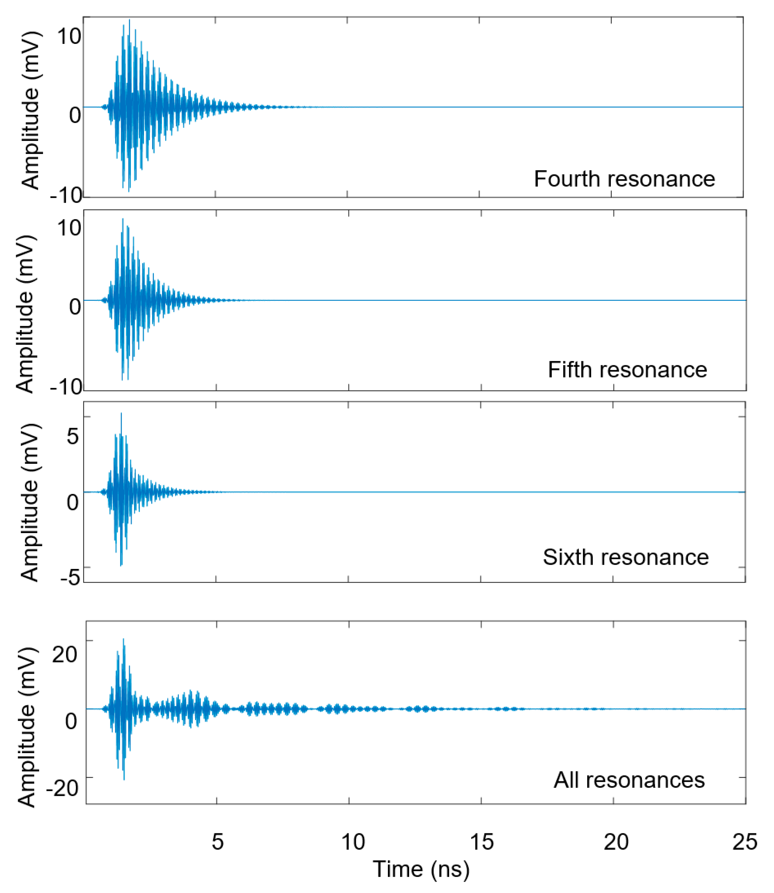
Through seven simulation steps for different conditions, including a no resonance scenario, the first to the sixth active resonances, the antenna-mode RCS responses are extracted and shown in Figure 6. For instance, to extract the antenna-mode response of the second resonance, a tag with only one active resonance (second resonator) was simulated, and the antenna-mode component was extracted by subtracting the antenna reflection and the reference structural-mode RCS component.
It can be noted that the lowest-frequency resonance (the first resonance) has the most protracted decay in the time domain, as shown in Figure 6, while the higher frequency responses such as the sixth resonance damp in a shorter time. In addition, the amplitude of the first and the last resonators are the lowest among all six resonances as they are the inner and outer resonators. The amplitude of the responses from the mid-band resonators is higher due to the presence of the coupling effect between adjacent resonators. The spread of the time domain resonances of the lower frequency resonators has also agreed with higher Q-factor transfer functions of those resonators in the frequency domain.
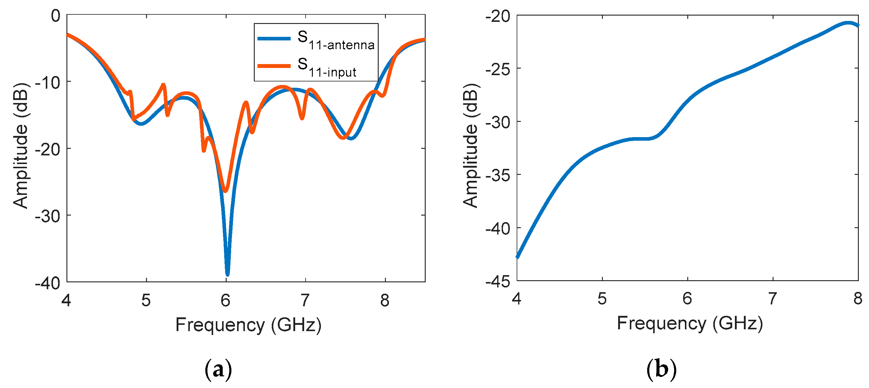
Besides the discussed time-domain response of the tag, the frequency response of the received signal is also demonstrated in Figure 7 and Figure 8. The captured input impedance RL vs. frequency plot of the antenna, without and with the tag in front of the antenna, (blue and red, respectively) are shown in Figure 7a. It can be seen that due to the loading effect of the tag, the RL is modulated with six resonances.
The structural-mode RCS was produced based on the simulation data in which the short-circuited tag was placed in the system. The captured data were calibrated with the RL to extract the structural-mode RCS. The frequency-domain extracted structural-mode RCS is shown in Figure 7b. As can be seen, there is an increment of the reflection from the copper and substrate of tag over the frequency band. This variation is basically related to the RCS level of the structure, which is frequency-dependent [38]. The minor fluctuation in the structural mode RCS is due to the shape of the resonators, which are partially filled by copper for resonance cancelation purposes.
The amplitude vs. frequency plot of the antenna-mode RCS of the individual resonator and their combined response as a 6-bit chipless RFID tag are depicted in Figure 8a,b, respectively. Noticeably, the individual resonators act as bandpass filters with a sharper transition in the lower frequency band as expected. Figure 8b depicts all the resonators’ frequency responses in the extracted antenna mode and background subtracted of the 6-bit tag. The response perfectly matches with the individual ones with a slight frequency shift and RCS level variations. The demonstrated antenna-mode, compared to the background subtraction, has only sharper peaks with more consistent RCS variations.
Table 1 compares the resonance frequency, 3-dB bandwidth, quality factor, differential amplitude between peak and null, and group delay (gradient dA/dω) for individual resonators and the 6-bit tag. The figures are provided when each resonator is present individually. The same information is provided for each resonator when combined in a 6-bit chipless RFID tag.
By comparing the information from these two scenarios, it is noticeable that after combining the resonators, a slight frequency shift to a lower frequency band has happened for all the resonances, while the quality factor of all resonances increased significantly. Moreover, the variation of RCS levels between the peak and the null of each resonance reduced slightly after the combination, whereas the group delay (slope) had an increment and decrement for different resonances. Overall, based on the geometry of the U-slot resonator tag, due to the coupling effect, the mentioned variation is as expected. The reason for this coupling effect is that, except for the first and last resonators, each slot is affected by the adjacent two resonators. Therefore, the activation/deactivation of resonators can affect the performance of its adjacent resonators slightly.
3.2. Equivalent Circuit Model
After the successful examination of the captured signal from a chipless RFID tag in CST simulation, the equivalent circuit model of the tag has been verified. Based on the characteristics of the actual individual resonators, the transfer functions of the resonators were estimated. The estimated coefficients and of the transfer function (7) of each individual resonator is demonstrated in Table 2. The selected tag consists of six U-slot resonators. The i-th resonator has a total length of , and a line width of W.
The performance parameters of the resonators are the resonance frequency, the quality factor, the spacing between the peak and null, and the depth of resonance in transition between peak and null. These characteristics also depend on the configuration of the resonator and the material of the substrate. Using the physical parameters of each resonator the equivalent inductor , resistance , and capacitor are calculated (Table 2). Furthermore, based on the actual resonance frequency and the quality factor, the coefficients of the transfer function are estimated. The frequency response of the individual reconstructed resonances, and their summation, are demonstrated in Figure 9. By comparing the actual individual response (Figure 8b) with the reconstructed one based on the model, it can be seen that with a good approximation, the resonators could be constructed from the suggested transfer function. The difference between their patterns is in the out of band rejection at a higher frequency of each resonance, which has a lower value in the actual resonances, and a higher value in the second-order assumed bandpass filter. However, in the combined resonances, this effect disappears, and the total antenna-mode RSC is estimated within an acceptable error margin.
In addition to that, the time-domain response of each resonator and the combined antenna-mode RCS component are calculated based on the proposed model. The constructed antenna-mode component based on the model is demonstrated in Figure 10. It can be seen that the pattern of individually constructed time-domain resonances is very similar to the simulated ones.
As expected, the time duration of the lower frequency resonances is much longer than the time duration of higher frequency resonances. Spreading the signal in the time domain can be interpreted based on the group delay. Table 2 shows that resonances with lower frequency have a higher group delay value. Moreover, the signal is spread in the time domain for a longer period of time.
The combined time-domain response of the six resonators is depicted in Figure 10. By comparing the result with the simulated response, it can be seen that there is a difference in amplitude and the pattern due to the minor errors of the individual resonator response, neglecting the coupling effect. However, the overall agreement between the two results is appropriate for justifying the validity of the model.
3.3. Time-Domain of the Equivalent Model
In addition to the evaluation of the time-domain model, the coefficients of the time-domain model envelope are extracted and compared to the simulation antenna-mode response for the third resonance, as shown in Figure 11. In this figure, the envelope of the modeled time-domain signal was compared to the simulated result for the third resonance. The modeled time-domain transfer function of this resonance is
where f is the center frequency of the third resonance with a value of 5.699 × 10⁹ Hz, is the time delay for arrival of the peak response with a value of 2.35 ns, and and are the rising and falling coefficients, and have values of 0.016 and 0.095, respectively, for this resonance response.
3.4. Measurement Results
A fabricated 6-bit U-slot tag was measured in Monash Microwave Antenna RFID and Sensor laboratory. This tag has the same characteristics as the 6-bit tag, which was studied in this paper. However, there is a difference between the resonance frequency positions of the fabricated tag, compared to the simulated one, due to fabrication error. Regardless of the slight frequency shifts of resonances, the simulation and measurement results can be compared. A photo of the tag and the measurement setup is demonstrated in Figure 12. The measurement setup consists of a commercialized vector network analyzer (VNA) operating as the reader, a UWB aperture coupled patch antenna, and the tag. Since the reflection from the environment was not included in the model, a few pieces of absorber foams were utilized in the measurement to reduce the reflection from the environment. In this case, the result of simulation and measurement can be compared with each other.
The measurement was conducted in two stages. Firstly, the return loss of the antenna was measured in the absence of the tag. Then, the tag was placed 5 cm apart from the antenna, and the return loss of the antenna was measured (called the input signal). For the first part of the study, based on the conventional background subtraction technique, the difference between these two measured vectors was calculated to achieve the reflection from the tag. Both vectors were also stored for generating time-domain signals and investigating the time gating performance.
The measured data from the VNA were in the form of S-parameters. At two stages of the measurement in this single antenna setup, the vectors were measured. The measured return loss of the antenna vs. frequency, in the absence of the tag, and in the presence of the tag, , are demonstrated in Figure 13a. It can be seen that the two plots have a similar pattern, with only a slight difference due to the loading effect of the tag. The reflection from the tag was achieved after reducing the effect of antenna reflection from the input signal, as shown in Figure 13b. Six resonances occurred with a sharp transition between peaks and nulls. The effect of noise in the system is shown as a noisy signal modulated to the original frequency signature.
Although a few pieces of absorber foam were placed around the tag, a negligible amount of reflection could still be added to the results caused by the plastic pole for supporting the tag. In addition to that, the reflection from the table, walls, ceil, and other items were included in the antenna return loss in the calibration measurement. The loading effect of the environment can be found by comparing the measured with the simulation antenna return loss in Figure 7a. Evidently, there is a significant frequency increase of the main resonance of the antenna from 6 GHz to 6.3 GHz, due to the loading effect of the environment.
Based on the frequency domain measured data, the time-domain signals were generated. The time-domain input signal, reflection from the antenna, and the processed signal after background subtraction are depicted in Figure 14, respectively. By comparing the input signal and the reflection from the antenna in the time domain, it can be noted that the time duration of the antenna reflection, with a dominant level, was up to 3.5 ns. However, the reflection from the antenna with components expanded to 8 ns. The amplitude of the antenna reflection is significantly higher compared to the tag reflection.
Figure 14 demonstrates that the reflection from the tag, including the antenna-mode and structural-mode components starts from 2 ns, which has the same time interval as a part of the antenna reflection component.
It can be seen that the tag RCS arrived with a longer delay, compared to the simulation one. This happened due to the created delay caused by the cable connecting the antenna with the reader in the measurement setup. In the simulation, the reflected signal was measured precisely at the port of the antenna, and any external response due to the reader hardware was excluded. As it is shown, there is an overlap on signals in the time domain for measurement in a short-range. Consequently, it can be concluded that time gating techniques applied to the input signal cannot be applicable for extracting the antenna-mode RCS in a short-range tag detection.
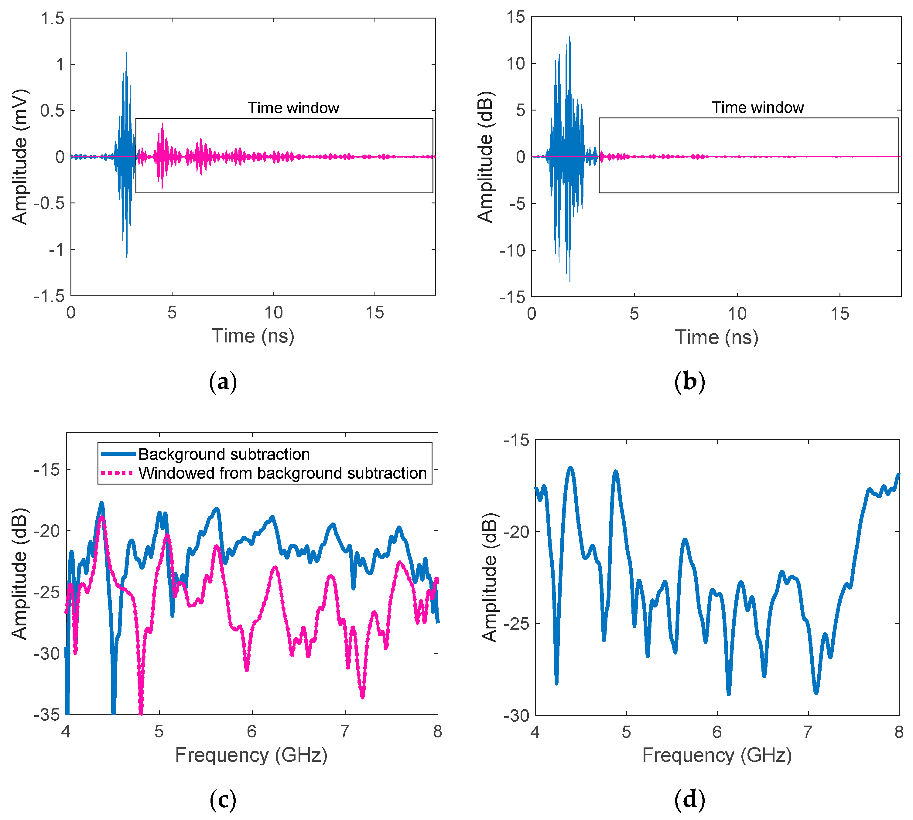
In order to investigate further, the antenna-mode structure of a measured signal from a tag placed at 7 cm was tested with two time-gating tests. The first attempt was applying an ideal rectangular time window to time-domain processed signal after background subtraction (Figure 15a) and secondly, applying the same window to the time-domain signal before background subtraction, as shown in Figure 15b. The frequency-domain responses for these two tests are shown in Figure 15c,d compared to the original background subtraction result. It should be noted that in the frequency domain response, the effect of the Gaussian pulse had been removed from the signals. As it can be seen, the time gating on the processed signal (background subtracted) gave a rough estimation of the resonance frequencies. Also, it could reduce the noise effect as well as improve the resonance quality factors for an easier tag ID detection in post-processing. On the other hand, in the frequency domain response of the time-gated input signal (Figure 15b) shows that there are some additional resonances in the signal due to the effect of the presence of some components of the reflection from the reader antenna. The unwanted resonances caused ambiguity in tag ID detection. In addition to that, the last resonance is missing in the results. This result demonstrates the weak point of time gating in short-range tag detection. Therefore, there is a need to have another technique signal processing for this problem.
A suggested signal processing algorithm to extract the antenna mode RCS from the signal is explained in [25] in which the unwanted signal components such as the structural mode RCS and the reflection from the reader antenna are estimated using a mathematical formula and are deducted from the signal. Then, the binary tag ID is extracted by analyzing the derivation of antenna mode RCS after compensation of the free space loss due to different reading ranges and the variation of the quality factor of different resonators. In this approach, the tag ID can be extracted regardless of the reading range.
4. Conclusions
This paper has analyzed the captured signal from a chipless RFID tag with a UWB antenna. The time and frequency domains signals from the reader antenna, the tag structure, and resonators were separated, and their different characteristics parameters such as resonant frequency, normalized RCS amplitude, differential peak/null amplitude, and group delays at resonances were calculated and examined. It was noticed that the reflection from the reader antenna created the strongest backscatter because it was received before being released from the antenna. The next strong component was the structural-mode RCS component of the tag. The last signal was the antenna-mode RCS, corresponding to the tag ID. Each resonator in the tag had a unique time and frequency domain signal. The starting points of the structural-mode RCS, amplitude, and time duration of the component were dependent on the physical parameters of the resonator, e.g., the resonant structure, reflection coefficient, group delay, and return loss of the resonator. It was seen that in a short-range tag measurement, all components in the captured signal overlapped in time domain as well as frequency domain. So, a time-frequency domain detection algorithm is required to extract the desired component.
The time gating technique was tested on the input signal and after background subtraction when the data were captured from a measured tag at a short distance (5 to 7 cm). It was concluded that applying time gating on the measured input signal from a tag in a very short-range tag detection is not an ideal approach due to the overlap of the antenna reflection with the desired components. On the other hand, time windowing after background subtraction helps to remove the effect of noise in the results as well as removing the structural-mode RCS response.
In addition, the equivalent circuit model of a multi-band resonator tag was proposed in this paper, and the model was verified with its simulation results in both time and frequency domains. The tag model can be used for a chipless RFID system model as well as in tag synthesis from the desired transfer function. For instance, the center frequency and the quality factor of a resonance can be found from the desired transfer function, then based on the suggested analysis, an estimation of the physical length of the resonator can be achieved.
Overall, the study has shown some light on understanding the backscattered signal from a frequency domain multi-bit chipless RFID tag, and demonstrates a research gap for future studies on tag detection for short-range applications.
Author Contributions
Conceptualization, F.B. and N.C.K.; data curation, F.B.; formal analysis, F.B.; investigation, F.B.; methodology, F.B.; resources, N.C.K.; supervision, N.C.K.; validation, F.B.; writing—original draft, F.B.; writing—review and editing, F.B. and N.C.K. All authors have read and agreed to the published version of the manuscript.
Funding
This work was supported in part by the Australian Research Council’s Linkage Grant (Discreet Reading of Printable Multi-Bit Chipless RFID Tags on Polymer Banknotes) under Grant LP130101044.
Acknowledgments
The authors would like to thank Lilian Khaw for her educational support in proofreading of this manuscript.
Conflicts of Interest
The authors declare no conflict of interest. The funders had no role in the design of the study; in the collection, analyses, or interpretation of data; in the writing of the manuscript, or in the decision to publish the results.
References
- Preradovic, S.; Karmakar, N.C. Chipless RFID: Bar Code of the Future. IEEE Microw. Mag. 2010, 11, 87–97. [Google Scholar] [CrossRef]
- Mulloni, V.; Donelli, M. Chipless RFID Sensors for the Internet of Things: Challenges and Opportunities. Sensors 2020, 20, 2135. [Google Scholar] [CrossRef] [PubMed] [Green Version]
- Martinez, M.; van der Weide, D. Compact single-layer depolarizing chipless RFID tag. Microw. Opt. Technol. Lett. 2016, 58, 1897–1900. [Google Scholar] [CrossRef]
- Pöpperl, M.; Parr, A.; Mandel, C.; Jakoby, R.; Vossiek, M. Potential and Practical Limits of Time-Domain Reflectometry Chipless RFID. IEEE Trans. Microw. Theory Tech. 2016, 64, 2968–2976. [Google Scholar] [CrossRef]
- Paredes, F.; Herrojo, C.; Mata-Contreras, J.; Moras, M.; Núñez, A.; Ramon, E.; Martín, F. Near-field chipless radio-frequency identification (RFID) sensing and identification system with switching reading. Sensors 2018, 18, 1148. [Google Scholar] [CrossRef] [Green Version]
- Babaeian, F.; Feng, J.; Karmakar, N. Realisation of a High Spectral Efficient Chipless RFID Tag using Hairpin Resonators. In Proceedings of the 2019 IEEE Asia-Pacific Microwave Conference (APMC), Singapore, 10–13 December 2019; pp. 114–116. [Google Scholar]
- Abdulkawi, W.M.; Sheta, A.-F.A.; Issa, K.; Alshebeili, S.A. Compact printable inverted-M shaped chipless RFID tag using dual-polarized excitation. Electronics 2019, 8, 580. [Google Scholar] [CrossRef] [Green Version]
- Ma, Z.; Jiang, Y. High-density 3D printable chipless RFID tag with structure of passive slot rings. Sensors 2019, 19, 2535. [Google Scholar] [CrossRef] [PubMed] [Green Version]
- Alam, J.; Khaliel, M.; Fawky, A.; El-Awamry, A.; Kaiser, T. Frequency-Coded Chipless RFID Tags: Notch Model, Detection, Angular Orientation, and Coverage Measurements. Sensors 2020, 20, 1843. [Google Scholar] [CrossRef] [Green Version]
- Nguyen, D.H.; Zomorrodi, M.; Karmakar, N.C. Spatial-Based Chipless RFID System. IEEE J. Radio Freq. Identif. 2019, 3, 46–55. [Google Scholar] [CrossRef]
- Vena, A.; Perret, E.; Tedjini, S. Chipless RFID Tag Using Hybrid Coding Technique. IEEE Trans. Microw. Theory Tech. 2011, 59, 3356–3364. [Google Scholar] [CrossRef]
- Babaeian, F.; Karmakar, N.C. Hybrid Chipless RFID Tags—A Pathway to EPC Global Standard. IEEE Access 2018, 6, 67415–67426. [Google Scholar] [CrossRef]
- Jiménez-Sáez, A.; Alhaj-Abbas, A.; Schüßler, M.; Abuelhaija, A.; El-Absi, M.; Sakaki, M.; Samfaß, L.; Benson, N.; Hoffmann, M.; Jakoby, R.; et al. Frequency-Coded mm-Wave Tags for Self-Localization System Using Dielectric Resonators. J. Infrared Millim. Terahertz Waves 2020, 41, 908–925. [Google Scholar] [CrossRef]
- Abbas, A.A.-H.; Abuelhaija, A.; Solbach, K. Investigation of the transient EM scattering of a dielectric resonator. In Proceedings of the 2018 11th German Microwave Conference, Freiburg, Germany, 12–14 March 2018; Volume 2018, pp. 271–274. [Google Scholar]
- Babaeian, F.; Karmakar, N. Development of Cross-Polar Orientation-Insensitive Chipless RFID Tags. IEEE Trans. Antennas Propag. 2020, 68, 5159–5170. [Google Scholar] [CrossRef]
- Abdulkawi, W.M.; Sheta, A.-F.A. K-State Resonators for High-Coding-Capacity Chipless RFID Applications. IEEE Access 2019, 7, 185868–185878. [Google Scholar] [CrossRef]
- Manekiya, M.; Donelli, M.; Kumar, A.; Menon, S.K. A novel detection technique for a chipless RFID system using quantile regression. Electronics 2018, 7, 409. [Google Scholar] [CrossRef] [Green Version]
- Babaeian, F.; Karmakar, N. A Cross-Polar Orientation Insensitive Chipless RFID Tag. In Proceedings of the 2019 IEEE International Conference on RFID Technology and Applications (RFID-TA), Pisa, Italy, 25–27 September 2019; pp. 116–119. [Google Scholar]
- Machac, J.; Polivka, M.; Svanda, M.; Havlicek, J. Reducing mutual coupling in chipless rfid tags composed of U-folded dipole scatterers. Microw. Opt. Technol. Lett. 2016, 58, 2723–2725. [Google Scholar] [CrossRef]
- Polivka, M.; Havlicek, J.; Svanda, M.; Machac, J. Improvement in Robustness and Recognizability of RCS Response of U-Shaped Strip-Based Chipless RFID Tags. IEEE Antennas Wirel. Propag. Lett. 2016, 15, 2000–2003. [Google Scholar] [CrossRef]
- Machac, J.; Boussada, A.; Svanda, M.; Havlicek, J.; Polivka, M. Influence of Mutual Coupling on Stability of RCS Response in Chipless RFID. Technologies 2018, 6, 67. [Google Scholar] [CrossRef] [Green Version]
- Kalansuriya, P.; Karmakar, N. Time domain analysis of a backscattering frequency signature based chipless RFID tag. In Proceedings of the Asia-Pacific Microwave Conference 2011, Melbourne, VIC, Australia, 5–8 December 2011; pp. 183–186. [Google Scholar]
- Rance, O.; Perret, E.; Siragusa, R.; Lemaitre-Auger, P. RCS Synthesis for Chipless RFID: Theory and Design; Elsevier: Amsterdam, The Netherlands, 2017. [Google Scholar]
- Aliasgari, J.; Karmakar, N.C. Mathematical Model of Chipless RFID Tags for Detection Improvement. IEEE Trans. Microw. Theory Tech. 2020. [Google Scholar] [CrossRef]
- Babaeian, F.; Forouzandeh, M.M.; Karmakar, N. Solving a Chipless RFID Inverse Problem Based on Tag Range Estimation. IET Microw. Antennas Propag. 2020. [Google Scholar] [CrossRef]
- Babaeian, F.; Karmakar, N.C. A High Gain Dual Polarized Ultra-Wideband Array of Antenna for Chipless RFID Applications. IEEE Access 2018, 6, 73702–73712. [Google Scholar] [CrossRef]
- Vena, A.; Perret, E.; Tedjini, S. Chipless RFID Based on RF Encoding Particle: Realization, Coding and Reading System; ISTE Press-Elsevier: London, UK; Oxford, UK, 2016. [Google Scholar]
- El-Hadidy, M.; El-Awamry, A.; Fawky, A.; Khaliel, M.; Kaiser, T. Real-world testbed for multi-tag UWB chipless RFID system based on a novel collision avoidance MAC protocol. Trans. Emerg. Telecommun. Technol. 2016, 27, 1707–1714. [Google Scholar] [CrossRef]
- Kalansuriya, P.; Karmakar, N.C.; Viterbo, E. On the Detection of Frequency-Spectra-Based Chipless RFID Using UWB Impulsed Interrogation. IEEE Trans. Microw. Theory Tech. 2012, 60, 4187–4197. [Google Scholar] [CrossRef] [Green Version]
- Ramos, A.; Perret, E.; Rance, O.; Tedjini, S.; Lazaro, A.; Girbau, D. Temporal Separation Detection for Chipless Depolarizing Frequency-Coded RFID. IEEE Trans. Microw. Theory Tech. 2016, 64, 2326–2337. [Google Scholar] [CrossRef]
- Vena, A.; Perret, E.; Tedjni, S. A Depolarizing Chipless RFID Tag for Robust Detection and Its FCC Compliant UWB Reading System. IEEE Trans. Microw. Theory Tech. 2013, 61, 2982–2994. [Google Scholar] [CrossRef]
- Hassanpour, H.; Zehtabian, A.; Sadati, S. Time domain signal enhancement based on an optimized singular vector denoising algorithm. Digit. Signal Process. 2012, 22, 786–794. [Google Scholar] [CrossRef]
- Islam, M.A.; Karmakar, N.C. A Novel Compact Printable Dual-Polarized Chipless RFID System. IEEE Trans. Microw. Theory Tech. 2012, 60, 2142–2151. [Google Scholar] [CrossRef]
- Santiago, J.M. Circuit Analysis for Dummies, 1st ed.; John Wiley & Sons: Hoboken, NJ, USA, 2013. [Google Scholar]
- Terman, F.E. Radio Engineers’ Handbook; McGraw-Hill: New York, NY, USA, 1943. [Google Scholar]
- Cohn, S.B. Slot line on a dielectric substrate. IEEE Trans. Microw. Theory Tech. 1969, 17, 768–778. [Google Scholar] [CrossRef]
- Salehi, M.; Manteghi, M. Transient Characteristics of Small Antennas. IEEE Trans. Antennas Propag. 2014, 62, 2418–2429. [Google Scholar]
- Ross, R. Radar cross section of rectangular flat plates as a function of aspect angle. IEEE Trans. Antennas Propag. 1966, 14, 329–335. [Google Scholar] [CrossRef]
Figure 1.
A back-scattered chipless radio frequency identification (RFID) resonator model.

Figure 2.
(a) A single U-shaped slot resonator; and (b) equivalent circuit.
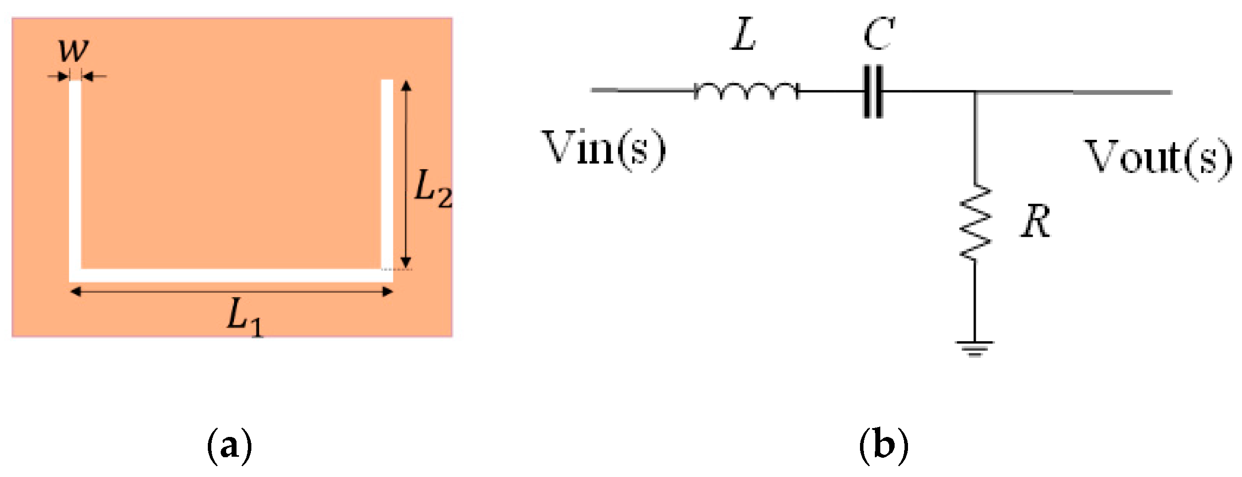
Figure 3.
(a) Simulation setup for a chipless RFID system when the tag was placed above the antenna with a spacing of 5 cm; (b) chipless RFID tag with U-shaped slots.
Figure 3.
(a) Simulation setup for a chipless RFID system when the tag was placed above the antenna with a spacing of 5 cm; (b) chipless RFID tag with U-shaped slots.
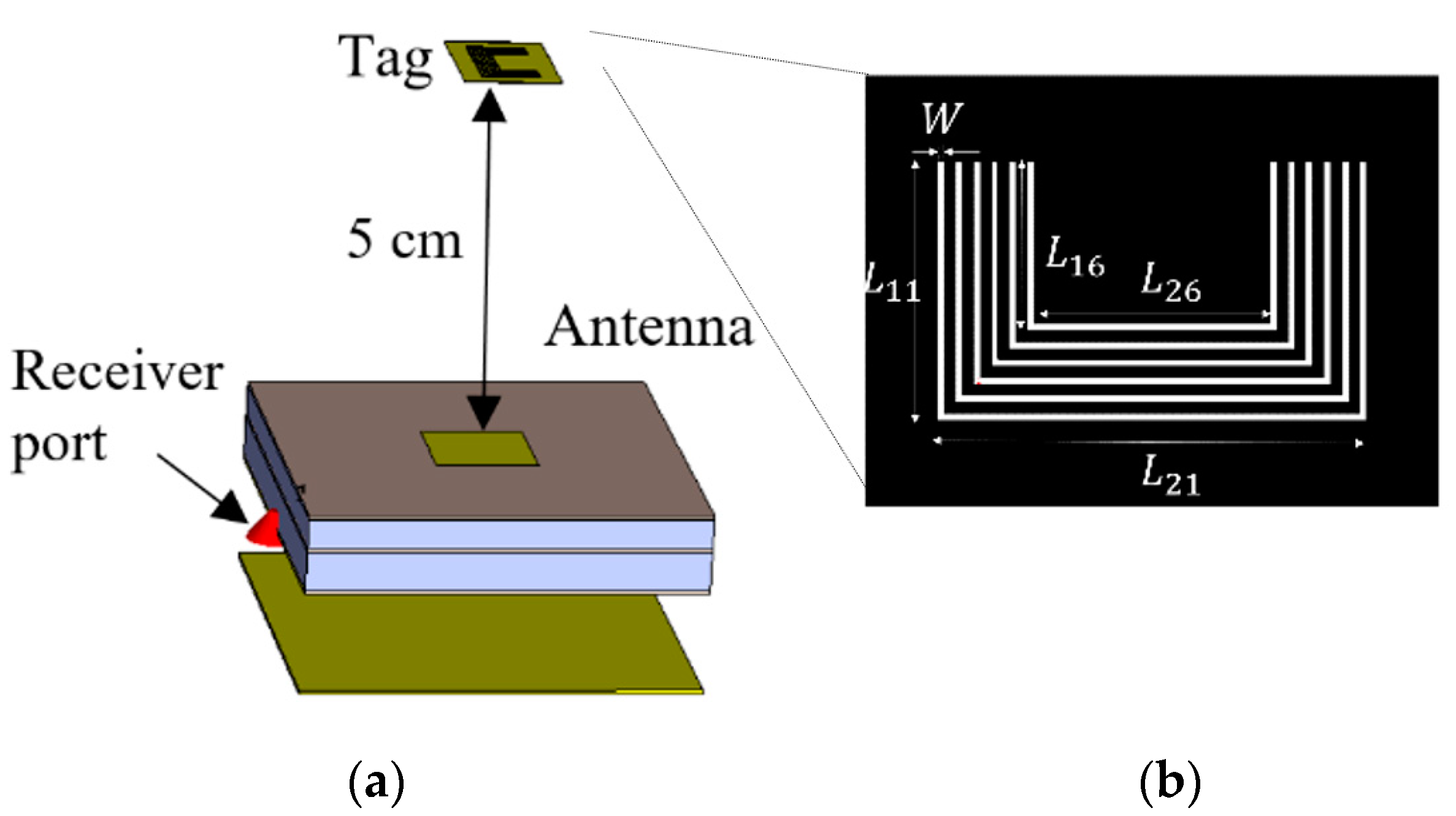
Figure 4.
Time-domain input signal and the processed signal after removing the reflection from the reader antenna.
Figure 4.
Time-domain input signal and the processed signal after removing the reflection from the reader antenna.
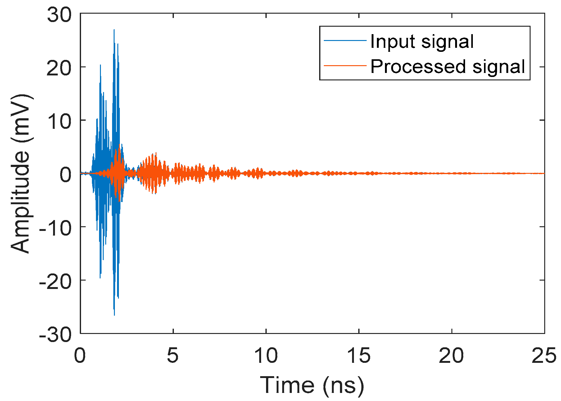
Figure 5.
Time-domain response of reader antenna reflection, tag structural-mode radar cross-section (RCS) component, and tag antenna-mode RCS component.
Figure 5.
Time-domain response of reader antenna reflection, tag structural-mode radar cross-section (RCS) component, and tag antenna-mode RCS component.

Figure 6.
Antenna-mode RCS of different resonances of the first, second, third, fourth, fifth, and sixth resonances.
Figure 6.
Antenna-mode RCS of different resonances of the first, second, third, fourth, fifth, and sixth resonances.
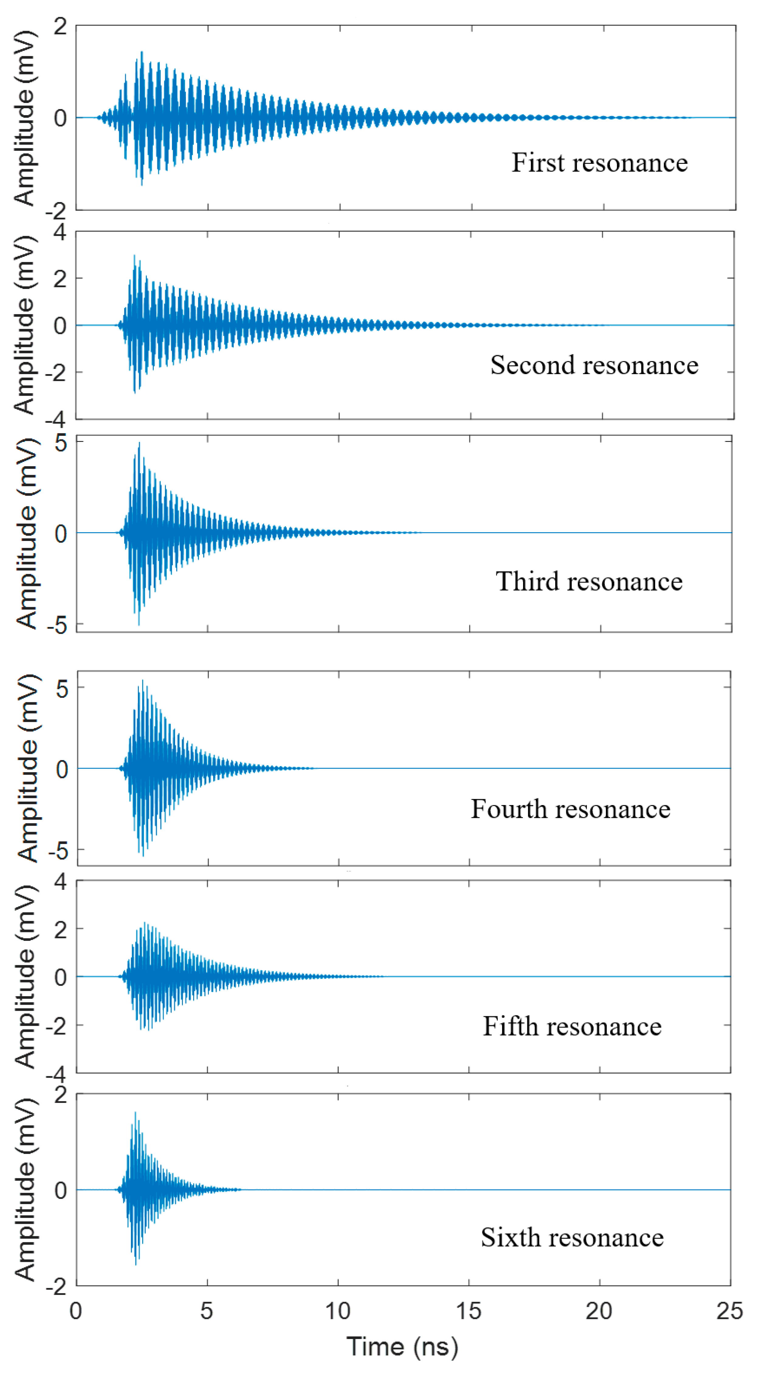
Figure 7.
Frequency domain. (a) Input signal when the tag is placed at 5 cm away from the antenna, and the return loss of the antenna; (b) structural-mode RCS of the tag.
Figure 7.
Frequency domain. (a) Input signal when the tag is placed at 5 cm away from the antenna, and the return loss of the antenna; (b) structural-mode RCS of the tag.

Figure 8.
(a) Antenna-mode frequency signature of individual resonators; (b) antenna-mode component of the 6-bit chipless RFID tag compared to the background subtraction.
Figure 8.
(a) Antenna-mode frequency signature of individual resonators; (b) antenna-mode component of the 6-bit chipless RFID tag compared to the background subtraction.

Figure 9.
Reconstructed (a) individual resonators; (b) combination of six resonators in a chipless RFID tag.
Figure 9.
Reconstructed (a) individual resonators; (b) combination of six resonators in a chipless RFID tag.
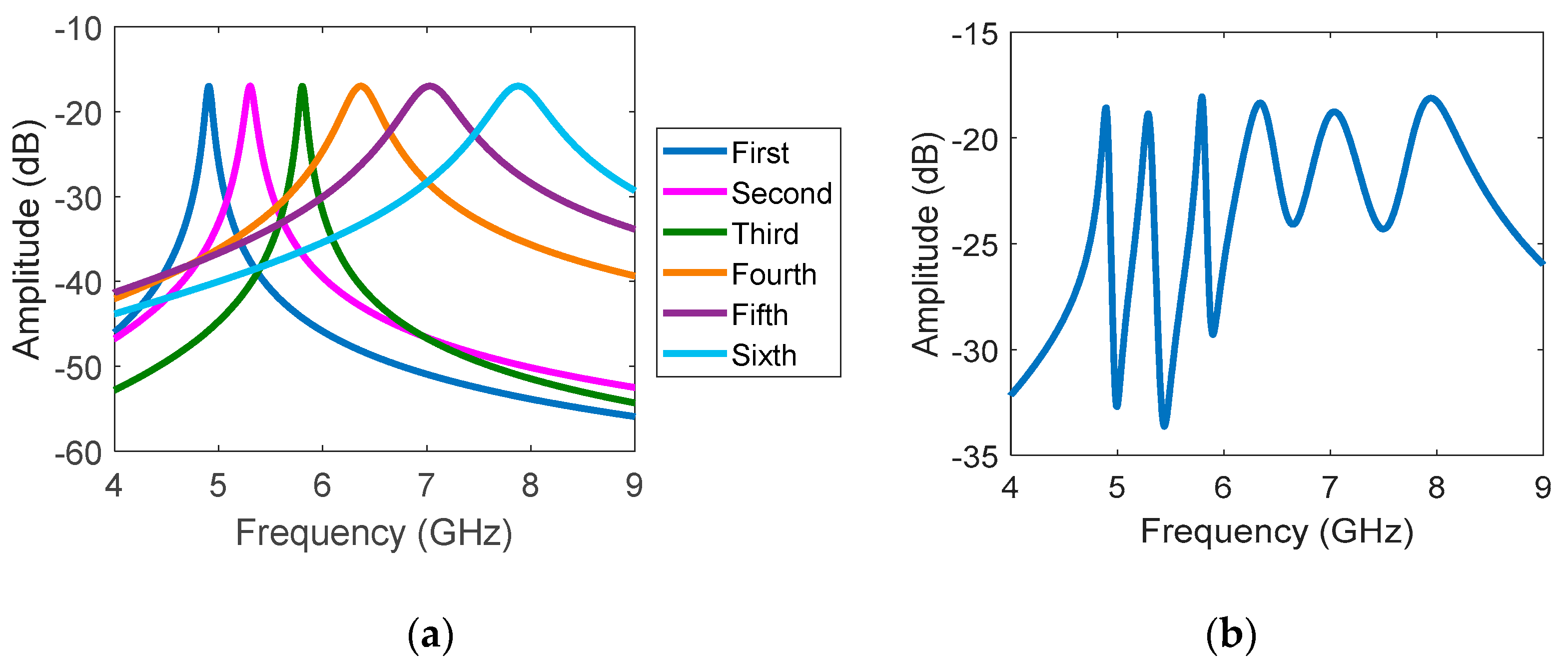
Figure 10.
Reconstructed time-domain response of the individual resonators based on the proposed model of the first, second, third, fourth, fifth, sixth resonators, and total tag.
Figure 10.
Reconstructed time-domain response of the individual resonators based on the proposed model of the first, second, third, fourth, fifth, sixth resonators, and total tag.
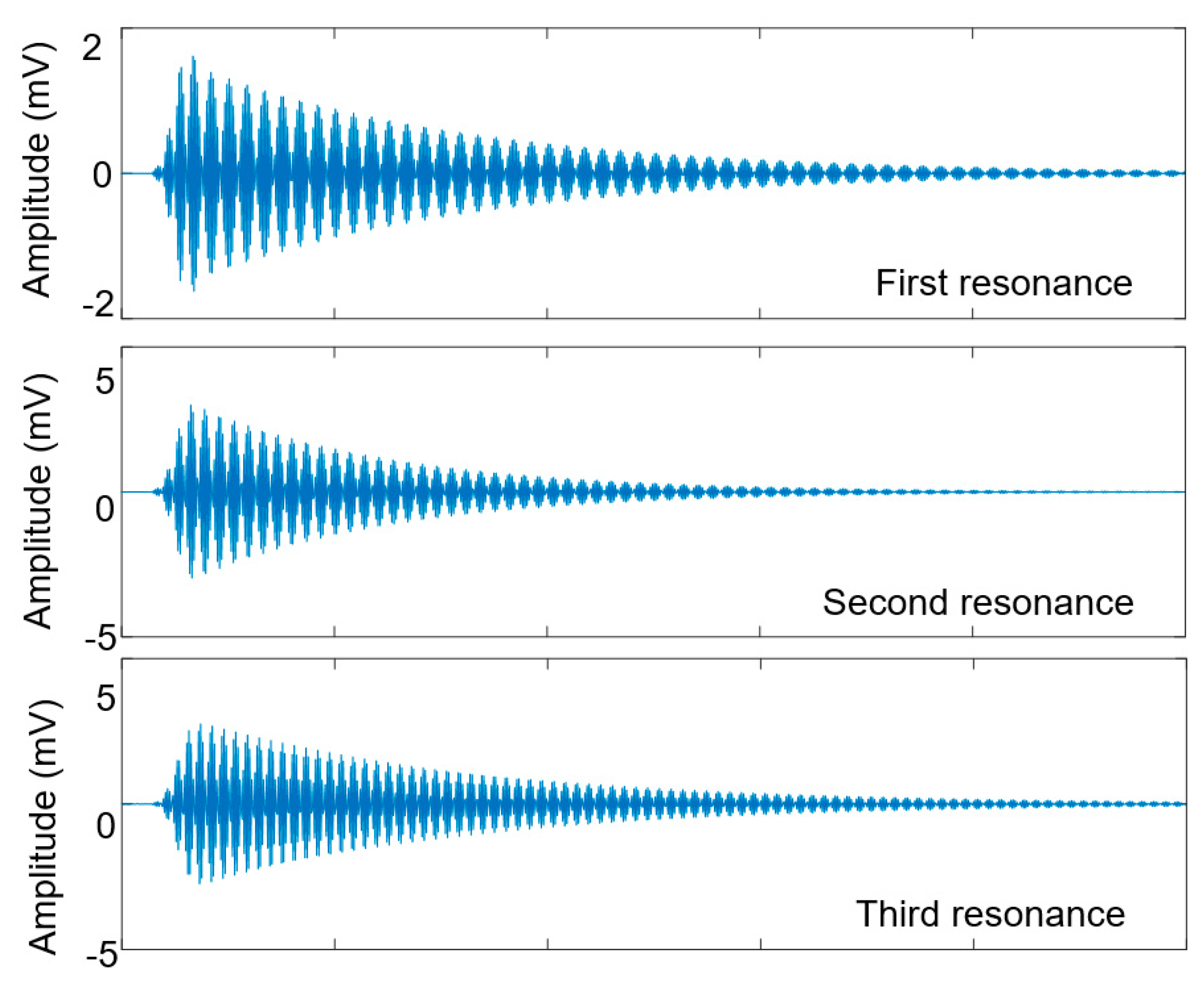

Figure 11.
Envelope of the time-domain model (y(t)) of the third resonance compared to the simulated result.
Figure 11.
Envelope of the time-domain model (y(t)) of the third resonance compared to the simulated result.

Figure 12.
Measurement setup and fabricated tag.
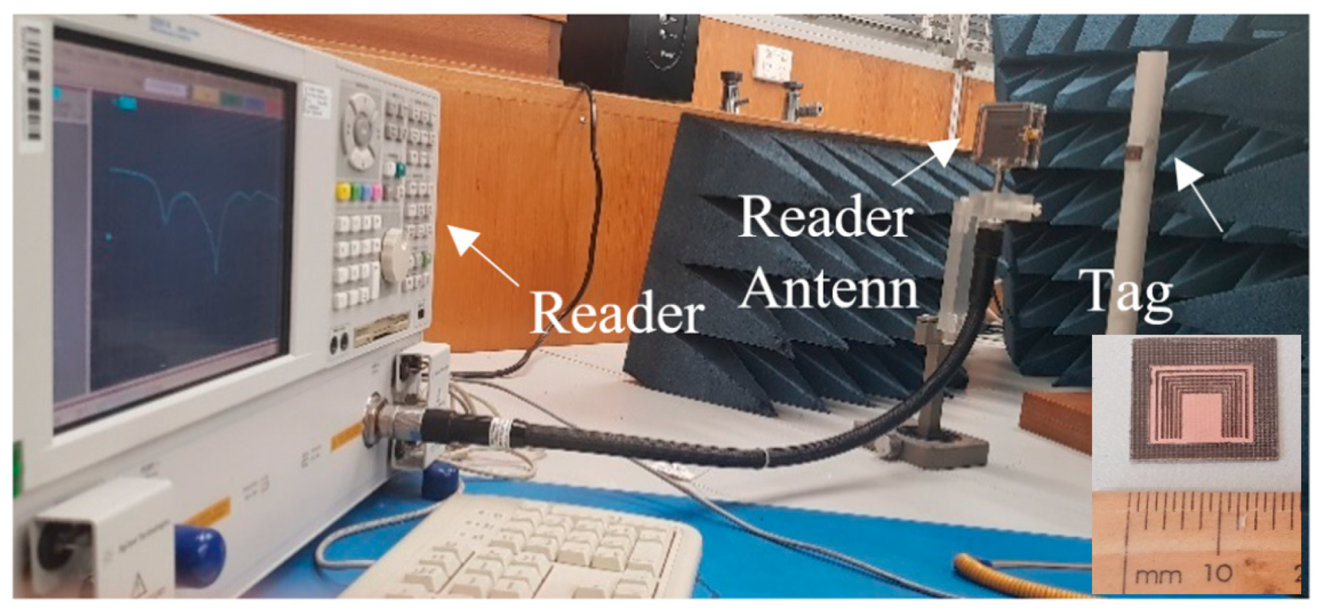
Figure 13.
(a) Return loss of the antenna in the absence and the presence of the tag; (b) Tag reflection based on background subtraction with smoothing.
Figure 13.
(a) Return loss of the antenna in the absence and the presence of the tag; (b) Tag reflection based on background subtraction with smoothing.

Figure 14.
Time-domain input signal, reflection from antenna, and processed signal.
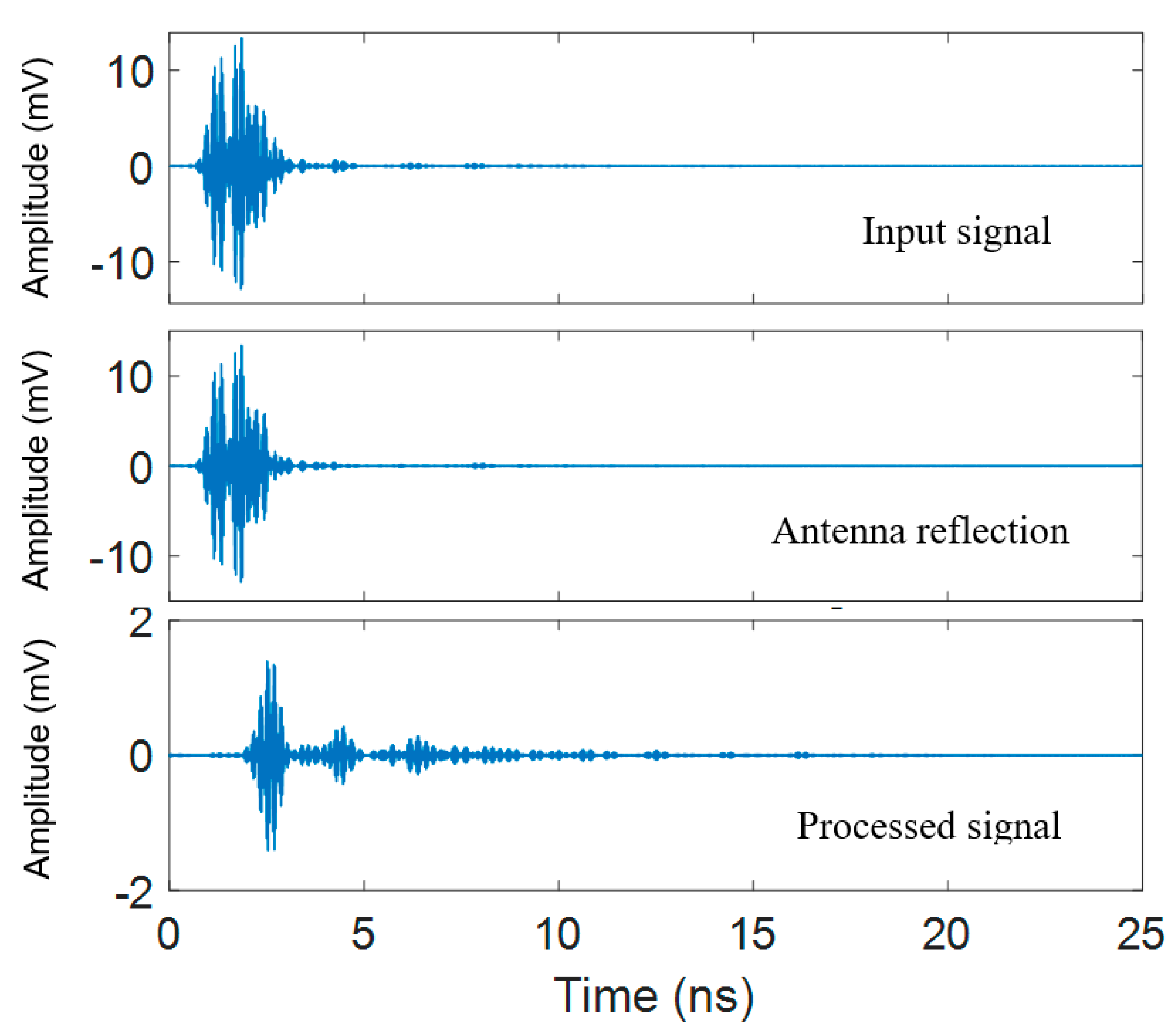
Figure 15.
(a) Time windowed from the input time-domain measured signal; (b) time windowed from the time-domain background subtraction signal; (c) comparison of the background subtraction, and time-gated from the background subtraction in frequency-domain; (d) frequency domain of directly time-gated signal from input signal.

Table 1.
Specification of individual and combined resonances.
| Individual Resonators | Combined Resonators | ||||||||||
|---|---|---|---|---|---|---|---|---|---|---|---|
| Order | Frequency (GHz) | 3-dB Bandwidth (MHz) | Q-Factor | Peak-Null Variation (dB) | Group Delay (ns) | Physical Length (mm) | Frequency (GHz) | 3-dB Bandwidth (MHz) | Q-Factor | Peak-Null Variation (dB) | Group Delay (ns) |
| 1st | 4.926 | 75 | 65.6 | 30.35 | 31.52 | 25.6 | 4.8 | 48 | 100 | 20.24 | 40.8 |
| 2nd | 5.34 | 98 | 54.4 | 21.18 | 25.87 | 23.6 | 5.22 | 64 | 81.5 | 19.76 | 36.57 |
| 3rd | 5.796 | 161 | 36 | 20.96 | 190 | 21.6 | 5.7 | 115 | 48.5 | 21.99 | 34.86 |
| 4th | 6.342 | 332 | 19.1 | 42.12 | 17.36 | 16.6 | 6.258 | 121 | 51.7 | 21.98 | 42.93 |
| 5th | 7.014 | 474 | 14.7 | 24.3 | 18.12 | 17.6 | 6.69 | 136 | 49.19 | 19.78 | 26.76 |
| 6th | 7.866 | 522 | 15 | 23.54 | 18.93 | 15.6 | 7.974 | 253 | 34.66 | 24.81 | 16.4 |
Table 2.
Equivalent circuit model parameters.
| Order | |||||
|---|---|---|---|---|---|
| 1st | 0.1098 | 0.0494 | 0.958 | 4.5 | 0.95 |
| 2nd | 0.0988 | 0.0613 | 0.912 | 6.2 | 1.11 |
| 3rd | 0.0880 | 0.0396 | 0.854 | 4.5 | 1.33 |
| 4th | 0.0622 | 0.1343 | 1.006 | 21.6 | 1.6 |
| 5th | 0.0672 | 0.215 | 0.763 | 32 | 1.95 |
| 6th | 0.0572 | 0.1887 | 0.714 | 33 | 2.45 |
© 2020 by the authors. Licensee MDPI, Basel, Switzerland. This article is an open access article distributed under the terms and conditions of the Creative Commons Attribution (CC BY) license (http://creativecommons.org/licenses/by/4.0/).
Share and Cite
MDPI and ACS Style
Babaeian, F.; Karmakar, N.C. Time and Frequency Domains Analysis of Chipless RFID Back-Scattered Tag Reflection. IoT 2020, 1, 109-127. https://doi.org/10.3390/iot1010007
AMA Style
Babaeian F, Karmakar NC. Time and Frequency Domains Analysis of Chipless RFID Back-Scattered Tag Reflection. IoT. 2020; 1(1):109-127. https://doi.org/10.3390/iot1010007
Chicago/Turabian StyleBabaeian, Fatemeh, and Nemai Chandra Karmakar. 2020. "Time and Frequency Domains Analysis of Chipless RFID Back-Scattered Tag Reflection" IoT 1, no. 1: 109-127. https://doi.org/10.3390/iot1010007