Supported and Suspended 2D Material-Based FET Biosensors


1
Department of Mechanical Engineering, Wayne State University, Detroit, MI 48202, USA
2
Department of Electrical and Computer Engineering, Wayne State University, Detroit, MI 48202, USA
*
Author to whom correspondence should be addressed.
Electrochem 2020, 1(3), 260-277; https://doi.org/10.3390/electrochem1030017
Submission received: 17 June 2020
/
Revised: 16 July 2020
/
Accepted: 20 July 2020
/
Published: 23 July 2020
Abstract
:Field Effect Transistor (FET)-based electrochemical biosensor is gaining a lot of interest due to its malleability with modern fabrication technology and the ease at which it can be integrated with modern digital electronics. To increase the sensitivity and response time of the FET-based biosensor, many semiconducting materials have been categorized, including 2 dimensional (2D) nanomaterials. These 2D materials are easy to fabricate, increase sensitivity due to the atomic layer, and are flexible for a range of biomolecule detection. Due to the atomic layer of 2D materials each device requires a supporting substrate to fabricate a biosensor. However, uneven morphology of supporting substrate leads to unreliable output from every device due to scattering effect. This review summarizes advances in 2D material-based electrochemical biosensors both in supporting and suspended configurations by using different atomic monolayer, and presents the challenges involved in supporting substrate-based 2D biosensors. In addition, we also point out the advantages of nanomaterials over bulk materials in the biosensor domain.
1. Introduction
The first biosensor was presented in 1962 by Clark and Lyons based on the enzyme electrode biochemical to detect chemical components present in blood [1]. Since then, a steep progression in bio-sensing technology has evolved, creating a significant impact on global human healthcare, environmental monitoring, drug delivery, and food safety [1]. The biosensor consists of a transducer that produces a measurable signal by varying physical or chemical properties of the active material. To date, there are various types of transducing mechanism investigated and commercialized amongst which optical, piezoelectric, and electrochemical are well known. In optical sensing, change in light absorption, reflection, and emission occur due to the variation in biomolecules [2]. Piezoelectric transducer works on the change in mass induced by the change in the concentration of bio-recognition event [3]. Lastly, electrochemical transducers comprise a change in the electrical impedance, potential, current, and modulation of the conductance by means of the sensing materials [4]. From these three types, electrochemical transducers are most popular due to the ease of fabrication, fast response time, portability, and low power consumption [5]. Electrochemical transducers can be further distinguished according to their electrical interface with the samples and electronics system, as shown in Figure 1. From these electrical interfaces, Field Effect Transistor (FET)-based devices are well known due to their excellent sensitivity and selectivity, and cost-effective wafer-scale fabrication.
1.1. General Operation of Field Effect Transistor (FET) Biosensor
Electrochemical field-effect transistor (FET)-based biosensors are attracting much attention due to their compatibility with electronic chips to achieve real-time data, low power consumption, label-free detection of specific biomolecules, and low-cost mass production. Traditional FETs consist of a semiconducting channel connected with two electrodes (source and drain) where gate electrodes manipulate channel conductance by using an electrostatic field called the gating effect. Generally, the gating effect is produced by applying a voltage through a metal gate electrode, which is capacitively attached with the semiconductor via a thin dielectric layer. However, in the case of a FET-based biosensor, a physical metal electrode is replaced by a specific receptor for selective target biomolecules. The trapped charged biomolecules generate a gating effect and change the conductivity of the channel, which is easily measured by transistor characteristics such as the source to drain current [3,4]. Silicon dioxide (SiO2) is usually used as a dielectric layer in transistors, but in biosensors, it is replaced by polymers and lipids, i.e., a bioreceptor, which can be easily functionalized on the semiconducting channel by using selective linkers as shown in schematic Figure 2. In addition, a reference electrode (such as Ag/AgCl, gold, silver or platinum) is used to apply the electrolyte gate voltage in electrochemical-based FET biosensor [6,7]. Generally, the reference gate electrode provides stable change in conductance as well as precise signal output, therefore, the reference electrode is one of the important elements in biosensor regime for steady and control operation [7,8,9].
For a semiconducting channel in FET-based biosensors, many materials have been categorized for better performance. These materials can be distinguished according to their structures, such as bulk, i.e., 3 dimension (3D), and nanomaterials, 0 dimension (0D), 1 dimension (1D), and 2 dimensions (2D). Among the two types of semiconducting materials, nanomaterials are attracting much attention because of their high surface to volume ratio that provides higher sensitivity. From all morphology of nanomaterials, 2D materials which have pristine structure can provide an excellent electrostatic effect due to the thin atomic layer [10]. In addition, 2D materials are easy to pattern due to planar structure, and dangling bond free surface, which is well suited as a semiconducting channel in FET than 1D and 0D materials. In the 2D domain, graphene has shown great potential since last decade because of its excellent electrical, optical, mechanical, and chemical properties [11]. After the great achievement of graphene, recently, interest in some new materials has emerged in 2D transition metal dichalcogenides (TMDs) such as MoS2, MoSe2, WS2, and WSe2 [12,13]. The properties of ultrathin 2D TMDs are intriguing fundamentally as well as technologically, in contrast to graphene, which is semi-metallic in nature, TMDs have a direct bandgap in monolayer and indirect in bulk [14]. Monolayer TMDs bandgap and carriers (n-type or p-type) can be tailored between compounds depending on their chemical composition [11,15]. Variation in the chemistry of different compounds and the crystal structure leads towards dramatic changes in their electronics properties.
Despite these merits, the performance and consistency of such atomic layer crystals are easily affected by supporting substrate interaction. This interaction of supporting substrate and atomic layer TMDs implies that the control of interface is vital for the performance and reliability of biosensor devices. Specifically, SiO2 substrate have highly disordered morphology and are chemically active due to the trapped atmospheric gases, chemical species, unidentified functional group, and electrostatic charges [16]. Therefore, transferring another layer of 2D TMDs on the top of SiO2 cannot contribute to charge transport clearly, which leads to the unreliable function of every single device. In recent years, many efforts have been made to enhance the quality of the substrate active layer interface such as using Poly(methyl methacrylate) (PMMA) and polymer electrolytes [10] which elude chemical bonding or surface roughness and improve mobility. However, PMMA and polymer electrolytes cannot be useful in specific applications such as 2D-based biosensor due to pristine coating of PMMA has the mean square roughness of 3.715 nm, which might introduce inconsistency on each fabricated device due to scattering phenomenon [17], whereas the polymer electrolyte vary the 2D semiconductor transport phenomenon and change its intrinsic properties [18,19]. Therefore, researchers have diverted towards the suspended 2D layer devices to take advantage of the intrinsic properties of 2D materials [20], which can be fabricated by wet etching of silicon dioxide (SiO2) underneath the monolayer [21]. Freestanding 2D TMDs have shown better performance than the supporting, on the SiO2 substrate in terms of back gating electronic conduction [22]. Therefore, this review illustrates the supported 2D material FET-based biosensor, challenges involved in supporting devices, and suspended-based biosensor and their fabrication method.
1.2. Interaction Mechanism between Semiconductor Material and Biomolecules
Many of the biochemical such as antibody-antigen [23,24], complementary single-stranded DNA [25], and enzyme interaction with substrate [26] are frequently used for harnessing signal from FET-based biosensors. The concentration of sensing biomolecule is directly proportion to the change in magnitude of the electrical signals from the FET [27]. When electrolyte solution interacts with device surface charge redistribution occurs and leads to change in surface potential. Figure 3 illustrates the potential-change phenomenon, which is influenced by the ionic strength and pH of the analyte solution. Solid–liquid interface can be best described by electrical double layer as shown in Figure 3a by Von Helmholtz [27,28]. This model was modified by Gouy equations:
where C0 and z are, respectively, the concentration of ions in the bulk solution and the valence of ions, is the permittivity of free space, is the dielectric constant of the solution, T is the temperature, k Boltzmann constant, and Ψ and Ψ0 are, respectively, the potential in each point in the solution and the potential at the interface solid/electrolyte [29]. Electrostatic double layer is a combination of Helmholtz model and the Gouy–Chapman model to describe the ion distribution in the Stern layer and the diffuse layer. Stern layer consists of two regions of inner and outer Helmholtz planes referred to respectively as inner Helmholtz plane (IHP) and outer Helmholtz plane (OHP) as shown in Figure 3b,c. The Debye length gives the thickness of the diffusion layer, the distance from the OHP into the solution up to the point where the electrostatic effect of the surface is felt by the ions [29]. The detection limit of biosensors is highly dependent with Debye screening length between the sensitive material surface and the electrolyte solution [30].
2. Nanomaterials in FET-Based Biosensor
As the material’s dimension reduces in the nanometer regime (1–100 nm), the surface to volume ratio, i.e., the ratio of surface atoms to the interior atoms is high. This type of structure is beneficial in the semiconducting channel of biological field effect transistor (Bio-FET) because of the external influence (electrostatic effect from the gate) that penetrates interior as well as surface atoms, as shown in Figure 4a,b. Therefore, a small change in the charged particles or biomolecules on the gate electrode brings a significant variation in conduction of nanomaterials, which can increase the sensitivity and reduce the detection limit. The atomic arrangement in the nanometer domain is confined, which reduces the internal scattering phenomenon of electrons and decreases the mean free path [31,32]. This advantageous atomic arrangement helps to enhance mobility as well as reduce the response time of detection. In addition, some nanomaterials are easily functionalized with the bioreceptor without any modification for specific detection of the biomolecule due to the tailoring of the wettability [10,33] Therefore, nanomaterials-based FET provides the best sensing platform by offering an excellent interface with bioreceptor, facilitates the binding of biomolecules, and reduces overall system power due to nano-level of operation.
The performance of nanomaterials in semiconducting channel depends upon the structure and the morphology, which are distinguished in 0D, 1D, and 2D. Each dimension exhibits unique properties that contribute tremendous potential in biosensing and bioelectronics applications. 0D and 1D are known as the first generation of the nanomaterials such as fullerene (C60), Carbon nanotubes (CNT), Silicon nanowires, gold nanoparticles, etc. These materials have shown better performance in FET-based biosensor by driving high current with small gate potential from charged particles and biomolecules [34]. Detection of the single-molecule and improvement of the sensitivity with these structures have been reported [35,36]. Despite the various merits of 0D and 1D, this technology is not successful in flourishing at biosensor domain due to low electronic mobility, difficulties in bandgap tuning, and this technology is also impossible to fabricate on large scale [37,38]. These flaws of the 1D and 0D nanomaterials are eliminated in 2D structure due to the pristine nature, compatible with recent nano/microfabrication, and easy to tune the bandgap [39,40,41].
2.1. 2 Dimensions (2D) Materials
In 2004, a single layer of graphite had been isolated by Andre Geim’s group at the University of Manchester, known as graphene [42]. Prompted by these, an ample number of reviews and articles have been published on 2D materials and its applications. The emergence of 2D materials has significantly changed the path of FET-based sensors. These materials are biocompatible, extremely sensitive, and feasible for batch mode fabrication. Patterning of 2D materials has further broadened the biosensor and bioelectronics applications. Numerous techniques for patterning of 2D materials have been recognized in the past decades [14,15,16,22,43]. It has just begun to apply a photolithography technique, electron beam lithography, and scanning probe technique for patterning 2D films [44,45,46,47]. Shortly the market for 2D materials is expected to compete with the reliability of silicon-based electronic sensor because of possibility of designing in micro and nanoscale. Furthermore, patterning these nanomaterials on various substrates holds promising development in healthcare wearable, and portable, flexible sensors [48,49]. In this section, properties of the various 2D materials are discussed along with the feasibility of the patterning as well as their potential application in the biosensor domain.
Various methods have been explored to achieve one atomic layer sheets. Micromechanical cleavage, also known as micromechanical exfoliation, is one of the techniques to get yielding films containing single and multiple layers of 2D materials [50]. Laser ablation and photo exfoliation are a controlled technique to achieve a 2D layer by removing material from the solid surface using laser beam [51]. Liquid-phase-exfoliation is a method to extract individual layers from solid materials in the liquid environment that involves three steps dispersion in a solvent, exfoliation, and purification [52,53]. Chemical vapor deposition (CVD) is a widely used method to achieve 2D monolayers and fabricate large area films of single to few layers [54,55]. This method is inexpensive and scalable to fabricate 2D material devices because of being easy to transfer on a non-specific substrate like SiO2/Si [56].
2.1.1. Graphene
Graphene is the first example of one atom thick layer of tightly bond sp2 carbon, which provides a whole new range of unusual properties for investigating, as shown in Figure 5a. Many of the extraordinary properties of graphene stem from its peculiar electronic bandgap and dimensionality in which the electrons mimic relativistic particle [57]. Therefore electrons in graphene are usually known as massless Dirac Fermions, which is ideally suitable to study the relativistic effect of condensed matter physics [58]. As shown in Figure 5b at a single point, the valence and the conduction band in graphene touch each other which compromise few electronics states near the Fermi level [59]. That is why graphene is usually called semi-metal or a zero bandgap semiconductor [60,61,62]. Single point contact makes graphene bandgap highly vulnerable to any change of electric field, doping, mechanical deformation, and adsorbates. This fragility of graphene bandgap opens the door to a new area in the sensing field [5,63,64].
2.1.2. Transition Metal Dichalcogenides (TMDs)
TMDs monolayer is one atom thick semiconductor, where atomic composition contains MX2 structure (M is a transition metal element from group IV, group V or group VI, whereas X is a chalcogen). As shown in Figure 6, TMDs form the layered structure of the arrangement X-M-X with two chalcogen atoms separated by transition metal atom in the hexagonal plane [65]. In semiconducting 2D TMDs, bulk layer possesses an indirect bandgap, whereas single layer contains direct gap. In case of Molybdenum disulfide (MoS2), the bulk indirect bandgap is 1.3 eV while single layer direct band gap is 1.8 eV [66,67]. This direct bandgap makes the MX2 semiconducting material suitable for many electronics and optoelectronic applications [68,69]. The most studied 2D TMDs is MoS2, which is similar to graphene and has a thickness equivalent to the unit cell, which is held by weak van der Waals forces. MoS2 planes contain molybdenum atoms sandwiched between two Sulphur atoms which demonstrate high electronic, mechanical, optical, and chemical properties [70,71]. Therefore, 2D TMDs such as MoS2 shows remarkable properties in the field of sensing applications [72,73]. 2D TMDs are mostly stable in a liquid as well as oxygen comprising environmental medium because its basal plane does not contain any dangling bonds, which facilitate their capable incorporation into sensing application [74]. Graphene and its oxides are semi-metallic, contain either no or negligible band gap which limits this material to make more sensitive sensors (mostly FET-based sensors). However, the overall sensitivity of device-based 2D TMDs, i.e., MoS2 is much more significant because of the existence band gap (1.8 eV) [75]. The band structure in 2D MoS2 contains d-orbital of Molybdenum in which 4 electrons from Mo fill the bonding state and the surface layers completed via lone pair of electrons [76,77]. The d-orbital hybridization of MoS2 leads towards the indirect to direct bandgap when it is exfoliated into a single layer [67,78]. It has demonstrated that a single layer MoS2 Field-effect transistor (FET) has turn ON/OFF ratio more than 108, which is specifically advantageous for highly sensitive FET-based sensors. The maximum free career mobility was estimated 400 cm2/Vs at room temperature whereas such high mobility of free carriers is impossible without high permittivity layers. The carrier lifetime of MoS2 is ~100 ps, and the diffusion coefficient is ~20 cm2/s [79]. This diffusion coefficient and carrier lifetime are apposite for making electrochemical and electric field-based sensors.
3. Supported 2D-Based FET Biosensor
Graphene and MoS2-based FETs are widely used in the biosensor domain; therefore, this section encompasses recent studies of these 2D materials supported on silicon di oxide (SiO2) substrate. A graphene-based selective FET biosensor was demonstrated by Yinxi et al., via detecting the E-coli bacteria [80]. Chemical Vapour deposition (CVD) grown graphene was functionalized by linkers and anti-E-coli to achieve specificity, as shown in schematic Figure 7a. It is interesting to notice that E-coli induce the hole on the graphene sheet and increase the conductivity on the left side of the Dirac point, as shown in Figure 7b. Drain current-gate voltage (ID-VLG) transfer curve of bare graphene, and functionalize steps of linkers, anti-E-coli, ethanolamine, and tween 20 is demonstrated in Figure 7c. Drain current-Drain voltage (ID-VD) performed at different concentration of E-coli bacteria was used to detect the limit of the sensor as illustrated in Figure 7d. The detection limit of graphene biosensor was found to be 10 CFU/mL, which varies from the conductivity of the graphene by 3.24%. This graphene sensor demonstrates high sensitivity, ease in fabrication, high response time, and label-free detection, which demonstrates that 2D materials have potential in the next generation of biosensing [7,81,82]. However, the absence of a bandgap in graphene makes this material unsuitable in the semiconductor field. In case of the small bandgap/semi-metallic semiconductors, electrons can tunnel through barrier very easily and increase the leakage current and reduce the performance of the sensor by increasing the subthreshold swing [83]. Thus, researchers are diverted their interest to other 2D single layer semiconducting materials with appropriate bandgap to turn ON/OFF devices and have negligible leakage current [84]. Specifically, considerable attention has been centering on the single-layer semiconducting materials, such as TMDs monolayer. 2D TMDs demonstrates very unique properties in the physical, optical, and electrical domains [85,86].
Figure 8a shows the schematic of the MoS2-based FET biosensor, where the first-time dielectric layer has functionalized with bio-receptors rather than the active material (2D materials) [38]. The direct functionalization of biomolecules (linkers and antibodies) on dielectric materials eliminates defects and considerable variation in semiconductor channel [82,87,88]. In other words, when linkers/antibodies are directly attached to the bare channel, the transduction mechanism is the combination of the electrostatic gating, direct charge transfer, and mobility modulation. The combination of the gating effect can provide false results and does not measure the real concentration of the target molecules. Therefore, it is desirable to eliminate the density of defects by covering bare channel material with insulating material and then functionalize linkers and antibodies on the top of the insulator [5]. In such type of the architecture of FET biosensor, Sarkar et al. has demonstrated highly sensitive and selective 2D FET-based sensor. In this paper, mechanically exfoliated MoS2 was transferred on the top of Silicon/Silicon di oxide substrate and then gold contacts were engraved to achieve source and drain. For gating purposes, Hafnium Oxide (HfO2) was used as a dielectric layer, where gate voltage was provided by ionic liquid. Sarkar et al. has depicted the pH sensing with 723 µA/pH sensitivity and for selective sensing, HfO2 was functionalized with 3-aminopropyl(triethoxy)silane (APTES) molecules and detection of the streptavidin has performed. The sensitivity through the MoS2-based FET biosensor was demonstrated 196 µA for 100 fM of the streptavidin at the subthreshold region (SS) as illustrated in Figure 8b,c [38].
4. Scattering Phenomenon in 2D Materials FET Devices
The 2D material has the potential to create a significant impact on a large number of applications ranging from electronics to the energy system, catalysis, new generation sensors, etc. A large number of patents and articles are coming from the field of the 2D materials regarding synthesis, physical properties, and their applications. When graphene was added in the 2D material family, it shows incredible achievement in the area of material science [63]. Then, other 2D materials have been investigated such as MoS2, tungsten disulphide (WS2), phosphorene, and boron nitride (BN), that have a unique bandgap structure, chiral fermions, biocompatibility, and rendering the quasiparticle in it formally identical to massless [58]. These properties of the 2D materials can be useful in real applications such as FET-based biosensors by enhancing the sensitivity and reliability of detection at low power [89]. However, the plane of the 2D layer has confined the transport and scattering of the carriers [90]. The following primary scattering mechanism affected the mobility of the carriers: (a) acoustic and optical phonon scattering; (b) surface interface phonon scattering; (c) Coulomb scattering at charge impurities; (d) roughness scattering. The amount of scattering phenomena affect the carrier transport governs the thickness of the layer, temperature, carrier density, effective mass, phonon, and electronic band structures [91].
4.1. Challenges
Coulomb scattering is also one of the critical causes to reduce the mobility of electrons in 2D materials. This phenomenon happens because of random charge impurities located in the 2D material or on its supporting surface [92]. The dielectric environment can improve mobility, as demonstrated for graphene [93] as well as for MoS2 [94]. The bandgap and carrier concentration in the 2D material can be tailored by using ionic impurities, but the mobility reduces because of scattering, the choice of doping depends upon the specific device performance. However, in extremely thin 2D materials (single atomic layer), the effect of roughness scattering and surface phonon is significant [95,96]. Despite the different scattering phenomenon in 2D materials, the presence of substrate scattering confines the electron mean free path to less than a micron which considers the significant barrier to developing devices from these low dimensional materials [97,98]. Interface between low dimension material and supporting substrate plays a critical role in the performance of the sensing field or any other devices [99]. For instance, SiO2 is the standard substrate for 2D material device fabrication which seems highly disordered topographically and chemically as well as it may harbor atmospheric gases, unknown functional group, chemical adsorbates and charges along with corrugation. This type of interface distortion affects the repeatability of the sensor data and decrement of mobility disturbs the response time and sensitivity of detection.
4.2. Solutions for Scattering
The 2D material have always required the supporting substrate to fabricate a device due to atomic layer structure [100]. The surface of the supporting substrate is highly disordered topographically as well as chemically for such thin nanomaterials, which creates a scattering phenomenon and reduce the overall mobility and the consistency of the device [11]. Several attempts have been taken to increase the mobility of 2D nanomaterials by upgrading the substrate. The high dielectric medium can be useful to reduce coulombic scattering and increase the mobility of the film. Lin et al. have demonstrated by coating a thin layer of electrolyte PEO and LiClO4 on the supporting substrate underneath of 2D material, which increases the mobility and reduces the contact resistance in between supporting substrate and atomic layer [101]. Similarly, Bao et al. demonstrated that Poly(methyl methacrylate) (PMMA) could provide high dielectric support and enhance the mobility and transport of electron in the MoS2 monolayer by eliminating the chemical bonding and surface roughness at the supporting substrate interface [102]. On the other hand, the freestanding 2D materials in between electrodes can eradicate the interface issues such as trapping of charges and upgrade transport properties of carrier charges, which seems a promising strategy towards highly sensitive sensors and digital electronic devices [103].
5. Suspended 2D-Based FET
5.1. Fabrication Technique
It has been demonstrated that single and few layers of MoS2 encapsulated with the high dielectric layer on a supporting substrate is very useful for FET’s application [94,104]. However, substrate disorder topography, unknown functional group, chemical adsorbates reduce the conductivity of the 2D material. To abbreviate these consequences and achieve high conductivity in 2D MoS2, Jin et al. demonstrated suspended MoS2 FET on SiO2 substrate by means of e-beam lithography and etching of insulator layer i.e., SiO2 [105]. As shown in Figure 9 (Ia) Mechanical exfoliated MoS2 transferred on an n-doped SiO2/Si substrate (300 nm SiO2 thickness) followed by e-beam lithography to create metal electrode for electrical characterization. Then, to achieve suspended MoS2, oxide layer etched in BOE (Buffer Oxide Etch) solution has been carried out to etch away half of the oxide thickness as shown in Figure 9 (Ib). Afterward, suspended MoS2 device was carefully transferred in ethanol solution and then dried out in critical point dryer (CPD) as illustrated in Figure 9 (Ic). Figure 9 (II,Id) represents the schematic, SEM, and optical image of the final suspended device inbetween the gold electrode with AFM mapping. In this experiment, Jin et al. verified that the mobility of suspended MoS2 is 0.9 cm2/Vs and supported one is 0.1 cm2/Vs. The on/off ratio is improved an order of magnitude in the suspended one, i.e., 105 [105]. This process of wet etching of SiO2 underneath of 2D materials process has been employed in different ISFET sensor, where electrode spacing varies from the 1 µm to 2 µm.
5.2. Suspended Based FET Biosensor
Cheng et al. reported the enhanced performance of the suspended graphene FET in the aqueous solutions by increasing the transconductance and decreasing the noise level [106]. This suspended graphene device demonstrated as a real time and sensitive pH sensor and can detect holes or electrons in same device, which is very useful to fabricate sensitive flexible bioelectronics device by using 2D materials. As shown in Figure 10a, this device is fabricated by using mechanically exfoliated graphene single layer on the top of the SiO2/Si wafer (300 nm SiO2 thickness). For electrical contacts, source and drain electrodes were defined by means of e-beam photolithography on the top graphene monolayer, subsequently metallization with 5/70 nm of Cr/Au. For confining the electrolyte 100 mM potassium chloride and 10 mM phosphate (pH7), a PDMS (polydimethylsiloxane) chamber was placed on the top of the device. Ag/AgCl, reference electrode was incorporated for gating purpose. To characterize the effect of oxide substrate, in-situ etching technique has been developed for tracking the conductance, while etching as shown in Figure 10b,c shows the change in conductance before and after the etching. The trans-conductance of holes in this device reaches until 1 mS/V in linear operating mode due to electrolyte gating. It is found that the conductance of device is larger at negative gate voltage due to the depletion of hole carrier. When gate voltage starts increasing in positive side the conductance of device decreases until its Dirac point and then it starts to increase with accumulation of electron carrier showing n-type of graphene behavior. It explains that the conductance in the suspended graphene is more as compared to the supported one.
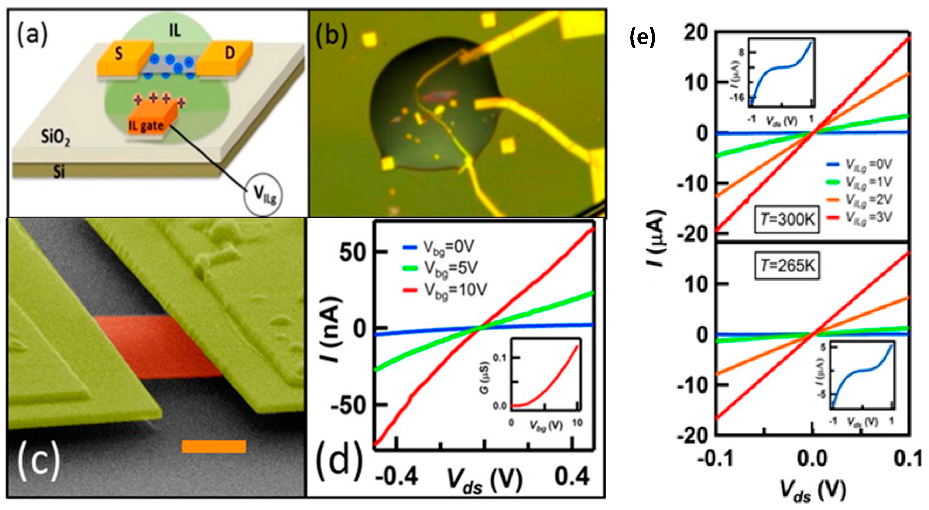
So it can work either as a p-type or n-type sensor when small gate voltage is applied without introducing of any chemical for redox reaction to change the carrier concentration of Graphene monolayer. The viability of this suspended graphene device in terms of pH sensing has been shown in Figure 10d, where pH solution varied from 6 to 9. From lower to higher pH value the conductance is consistently increased whereas the Dirac point is shifted towards the positive side with respective gate voltage. In Figure 10e, this device works as a p-type when negative potential is applied with different concentration of the pH value as well as n-type when gate potential is positive. Ionic liquid salt contains mobile ions (cations and anions), which are useful for ISFET sensing [107]. When an electric field is applied, ions in the liquid accumulate, forming an electric double layer on the top of the device by creating a nanogap capacitor with large capacitance. Ionic gating can induce charge density which is usually an order magnitude greater than the traditional back gating. Wang et al. demonstrated the effect of ionic gating in the suspended MoS2 monolayer [103]. In this case, they have eliminated the scattering effect comes from the SiO2/Si substrate as well as shown the top and bottom side of electric double layer gating. A droplet of ionic liquid deposited, as shown in the schematic of Figure 11a, and an optical image in Figure 11b. These devices are usually suspended after addition of the Ionic liquid (IL). In this device, the conductance of typically increase 103 or 104, and the enhanced mobility found 46 cm2/(V s). Fabrication process to achieve suspended layer is same as mentioned in above [103]. The mechanically exfoliated MoS2 sheet is coupled with Ti/Au electrodes and acquire free-standing layer by etching SiO2 in hydrofluoric acid, as shown in Figure 11c. Suspended MoS2 devices characterized in vacuum environment at room temperature as illustrated in Figure 11d, I-V characteristics at a different back gate voltage (mobility ~2.1 cm2/(V s)). A suspended IL gating device improves the performance regarding conductance increment in order of 103 or 104, and mobility of the device is 46 cm2/(V s). To recognize carrier transport mechanism in the fabricated devices by applying IL gating, Wang et al. measured their transfer curve characteristics at different gate voltage as shown in Figure 11e at temperature 300 K and 265 K. As gate voltage increased, the device conductance also improved from ~1 to ~180 μS, which indicates the Fermi level is shifted near to conduction band. As shown in Figure 11e inset at lower gate voltage I-V curves are linear, but it becomes nonlinear at higher gate voltages. This IL gating suspended devices demonstrate such a drastic enhancement in conduction, which suggests that IL reduces the Schottky barrier at the interface of metal and the semiconductor. Additionally, the improvement in mobility indicates that charge impurities reduced because of the IL help to reduce electron scattering. These types of structure are very suitable for building the suspended reliable pH sensor.
6. Conclusions
Among various 2D materials, TMDs has demonstrated impressive performance in FET-based biosensor because of the tunable bandgap, biocompatibility, and high mobility. The nanometer thickness of these materials requires supporting substrate (SiO2/Si) to fabricate the FET devices. However, supporting substrate has uneven morphology, harbor atmospheric gases, unknown functional group, corrugated charges, and chemical adsorbates, which degrades the transport properties of the 2D materials by scattering phenomenon. This effect implies that the interface control between 2D material and the supporting substrate is essential due to the unreliability output response from every single fabricated sensor. To solve these issues, freestanding 2D materials without interacting with the supporting substrate are viable, which have shown improvement of carrier transport as compared to the supporting substrate.
Author Contributions
N.M.: manuscript preparation; N.M., L.M.R.A. and S.V.: reviewing and evaluating of different 2D materials papers for manuscript; N.M. and S.V.: figures preparation and copyright permission. All authors have read and agreed to the published version of the manuscript.
Funding
This research received no external funding.
Conflicts of Interest
The authors declare no conflict of interest.
References
- Neethirajan, S.; Tuteja, S.K.; Huang, S.-T.; Kelton, D. Recent advancement in biosensors technology for animal and livestock health management. Biosens. Bioelectron. 2017, 98, 398–407. [Google Scholar] [CrossRef]
- Haes, A.J.; Van Duyne, R.P. A nanoscale optical biosensor: Sensitivity and selectivity of an approach based on the localized surface plasmon resonance spectroscopy of triangular silver nanoparticles. J. Am. Chem. Soc. 2002, 124, 10596–10604. [Google Scholar] [CrossRef] [PubMed]
- Babacan, S.; Pivarnik, P.; Letcher, S.; Rand, A. Evaluation of antibody immobilization methods for piezoelectric biosensor application. Biosens. Bioelectron. 2000, 15, 615–621. [Google Scholar] [CrossRef]
- Say, J.; Tomasco, M.F.; Heller, A.; Gal, Y.; Aria, B.; Heller, E.; Plante, P.J.; Vreeke, M.S. Process for Producing an Electrochemical Biosensor. U.S. Patent 6,103,033, 15 August 2000. [Google Scholar]
- Shao, Y.; Wang, J.; Wu, H.; Liu, J.; Aksay, I.A.; Lin, Y. Graphene based electrochemical sensors and biosensors: A review. Electroanal. Int. J. Devoted Fundam. Pract. Asp. Electroanal. 2010, 22, 1027–1036. [Google Scholar] [CrossRef]
- Sarkar, D.; Banerjee, K. Proposal for tunnel-field-effect-transistor as ultra-sensitive and label-free biosensors. Appl. Phys. Lett. 2012, 100, 143108. [Google Scholar] [CrossRef]
- Lee, J.; Dak, P.; Lee, Y.; Park, H.; Choi, W.; Alam, M.A.; Kim, S. Two-dimensional layered MoS2 biosensors enable highly sensitive detection of biomolecules. Sci. Rep. 2014, 4, 7352. [Google Scholar] [CrossRef] [Green Version]
- Liu, Q.; Liu, Y.; Wu, F.; Cao, X.; Li, Z.; Alharbi, M.; Abbas, A.N.; Amer, M.R.; Zhou, C. Highly sensitive and wearable In2O3 nanoribbon transistor biosensors with integrated on-chip gate for glucose monitoring in body fluids. ACS Nano 2018, 12, 1170–1178. [Google Scholar] [CrossRef]
- Kang, P.; Wang, M.C.; Nam, S. Bioelectronics with two-dimensional materials. Microelectron. Eng. 2016, 161, 18–35. [Google Scholar] [CrossRef] [Green Version]
- Boguslavsky, Y.; Fadida, T.; Talyosef, Y.; Lellouche, J.-P. Controlling the wettability properties of polyester fibers using grafted functional nanomaterials. J. Mater. Chem. 2011, 21, 10304–10310. [Google Scholar] [CrossRef]
- Zhu, W.; Perebeinos, V.; Freitag, M.; Avouris, P. Carrier scattering, mobilities, and electrostatic potential in monolayer, bilayer, and trilayer graphene. Phys. Rev. B 2009, 80, 235402. [Google Scholar] [CrossRef] [Green Version]
- Thanh, T.D.; Chuong, N.D.; Van Hien, H.; Kshetri, T.; Kim, N.H.; Lee, J.H. Recent advances in two-dimensional transition metal dichalcogenides-graphene heterostructured materials for electrochemical applications. Prog. Mater. Sci. 2018, 96, 51–85. [Google Scholar] [CrossRef]
- Guimaraes, M.H.; Gao, H.; Han, Y.; Kang, K.; Xie, S.; Kim, C.-J.; Muller, D.A.; Ralph, D.C.; Park, J. Atomically thin ohmic edge contacts between two-dimensional materials. ACS Nano 2016, 10, 6392–6399. [Google Scholar] [CrossRef] [PubMed] [Green Version]
- Bell, D.J.; Lu, T.; Fleck, N.A.; Spearing, S.M. MEMS actuators and sensors: Observations on their performance and selection for purpose. J. Micromech. Microeng. 2005, 15, S153. [Google Scholar] [CrossRef] [Green Version]
- Zhang, G.; Wang, D. Colloidal lithography—The art of nanochemical patterning. Chem. Asian J. 2009, 4, 236–245. [Google Scholar] [CrossRef]
- Stellacci, F.; Bauer, C.A.; Meyer-Friedrichsen, T.; Wenseleers, W.; Alain, V.; Kuebler, S.M.; Pond, S.J.; Zhang, Y.; Marder, S.R.; Perry, J.W. Laser and electron-beam induced growth of nanoparticles for 2D and 3D metal patterning. Adv. Mater. 2002, 14, 194–198. [Google Scholar] [CrossRef]
- Nathawat, R.; Kumar, A.; Acharya, N.; Vijay, Y. XPS and AFM surface study of PMMA irradiated by electron beam. Surf. Coat. Technol. 2009, 203, 2600–2604. [Google Scholar] [CrossRef]
- Vasu, K.; Chakraborty, B.; Sampath, S.; Sood, A. Probing top-gated field effect transistor of reduced graphene oxide monolayer made by dielectrophoresis. Solid State Commun. 2010, 150, 1295–1298. [Google Scholar] [CrossRef] [Green Version]
- Xu, H.; Fathipour, S.; Kinder, E.W.; Seabaugh, A.C.; Fullerton-Shirey, S.K. Reconfigurable ion gating of 2H-MoTe2 field-effect transistors using poly (ethylene oxide)-CsClO4 solid polymer electrolyte. ACS Nano 2015, 9, 4900–4910. [Google Scholar] [CrossRef]
- Lee, G.; Kim, S.; Jung, S.; Jang, S.; Kim, J. Suspended black phosphorus nanosheet gas sensors. Sens. Actuators B Chem. 2017, 250, 569–573. [Google Scholar] [CrossRef]
- Wang, F.; Stepanov, P.; Gray, M.; Lau, C.N. Annealing and transport studies of suspended molybdenum disulfide devices. Nanotechnology 2015, 26, 105709. [Google Scholar] [CrossRef]
- Cao, L.; Yang, S.; Gao, W.; Liu, Z.; Gong, Y.; Ma, L.; Shi, G.; Lei, S.; Zhang, Y.; Zhang, S. Direct laser-patterned micro-supercapacitors from paintable MoS2 films. Small 2013, 9, 2905–2910. [Google Scholar] [CrossRef] [PubMed]
- Lin, V.S.-Y.; Motesharei, K.; Dancil, K.-P.S.; Sailor, M.J.; Ghadiri, M.R. A porous silicon-based optical interferometric biosensor. Science 1997, 278, 840–843. [Google Scholar] [CrossRef] [PubMed]
- Stayton, P.S.; Shimoboji, T.; Long, C.; Chilkoti, A.; Ghen, G.; Harris, J.M.; Hoffman, A.S. Control of protein–ligand recognition using a stimuli-responsive polymer. Nature 1995, 378, 472–474. [Google Scholar] [CrossRef] [PubMed]
- Uslu, F.; Ingebrandt, S.; Mayer, D.; Böcker-Meffert, S.; Odenthal, M.; Offenhäusser, A. Labelfree fully electronic nucleic acid detection system based on a field-effect transistor device. Biosens. Bioelectron. 2004, 19, 1723–1731. [Google Scholar] [CrossRef]
- Lee, C.-S.; Kim, S.K.; Kim, M. Ion-sensitive field-effect transistor for biological sensing. Sensors 2009, 9, 7111–7131. [Google Scholar] [CrossRef]
- Zhang, L.L.; Zhao, X. Carbon-based materials as supercapacitor electrodes. Chem. Soc. Rev. 2009, 38, 2520–2531. [Google Scholar] [CrossRef]
- Helmholtz, H.v. On the conservation of force. Sci. Mem. 1862, 1, 114. [Google Scholar]
- Huang, W.; Diallo, A.K.; Dailey, J.L.; Besar, K.; Katz, H.E. Electrochemical processes and mechanistic aspects of field-effect sensors for biomolecules. J. Mater. Chem. C 2015, 3, 6445–6470. [Google Scholar] [CrossRef]
- Park, J.; Nguyen, H.H.; Woubit, A.; Kim, M. Applications of field-effect transistor (FET)-type biosensors. Appl. Sci. Converg. Technol. 2014, 23, 61–71. [Google Scholar] [CrossRef] [Green Version]
- Ramgir, N.S.; Yang, Y.; Zacharias, M. Nanowire-based sensors. Small 2010, 6, 1705–1722. [Google Scholar] [CrossRef]
- Ramnani, P.; Saucedo, N.M.; Mulchandani, A. Carbon nanomaterial-based electrochemical biosensors for label-free sensing of environmental pollutants. Chemosphere 2016, 143, 85–98. [Google Scholar] [CrossRef] [Green Version]
- Torchinsky, I.; Rosenman, G. Wettability modification of nanomaterials by low-energy electron flux. Nanoscale Res. Lett. 2009, 4, 1209. [Google Scholar] [CrossRef] [PubMed] [Green Version]
- Zhang, Y.; Duan, L.F.; Zhang, Y.; Wang, J.; Geng, H.; Zhang, Q. Advances in conceptual electronic nanodevices based on 0D and 1D nanomaterials. Nano Micro Lett. 2014, 6, 1–19. [Google Scholar] [CrossRef]
- Mazloum-Ardakani, M.; Khoshroo, A. High performance electrochemical sensor based on fullerene-functionalized carbon nanotubes/ionic liquid: Determination of some catecholamines. Electrochem. Commun. 2014, 42, 9–12. [Google Scholar] [CrossRef]
- Balasubramanian, K.; Burghard, M. Biosensors based on carbon nanotubes. Anal. Bioanal. Chem. 2006, 385, 452–468. [Google Scholar] [CrossRef] [PubMed]
- Shearer, C.J.; Cherevan, A.; Eder, D. Application and future challenges of functional nanocarbon hybrids. Adv. Mater. 2014, 26, 2295–2318. [Google Scholar] [CrossRef] [PubMed]
- Sarkar, D.; Liu, W.; Xie, X.; Anselmo, A.C.; Mitragotri, S.; Banerjee, K. MoS2 field-effect transistor for next-generation label-free biosensors. ACS Nano 2014, 8, 3992–4003. [Google Scholar] [CrossRef]
- Kang, K.; Lee, K.-H.; Han, Y.; Gao, H.; Xie, S.; Muller, D.A.; Park, J. Layer-by-layer assembly of two-dimensional materials into wafer-scale heterostructures. Nature 2017, 550, 229–233. [Google Scholar] [CrossRef]
- Mas-Balleste, R.; Gomez-Navarro, C.; Gomez-Herrero, J.; Zamora, F. 2D materials: To graphene and beyond. Nanoscale 2011, 3, 20–30. [Google Scholar] [CrossRef]
- Zhang, P.; Wang, F.; Yu, M.; Zhuang, X.; Feng, X. Two-dimensional materials for miniaturized energy storage devices: From individual devices to smart integrated systems. Chem. Soc. Rev. 2018, 47, 7426–7451. [Google Scholar] [CrossRef] [Green Version]
- Novoselov, K.S.; Jiang, D.; Schedin, F.; Booth, T.; Khotkevich, V.; Morozov, S.; Geim, A.K. Two-dimensional atomic crystals. Proc. Natl. Acad. Sci. USA 2005, 102, 10451–10453. [Google Scholar] [CrossRef] [Green Version]
- Li, X.; Cai, W.; An, J.; Kim, S.; Nah, J.; Yang, D.; Piner, R.; Velamakanni, A.; Jung, I.; Tutuc, E. Large-area synthesis of high-quality and uniform graphene films on copper foils. Science 2009, 324, 1312–1314. [Google Scholar] [CrossRef] [PubMed] [Green Version]
- Hu, K.; Tolentino, L.S.; Kulkarni, D.D.; Ye, C.; Kumar, S.; Tsukruk, V.V. Written-in Conductive Patterns on Robust Graphene Oxide Biopaper by Electrochemical Microstamping. Angew. Chem. Int. Ed. 2013, 52, 13784–13788. [Google Scholar] [CrossRef] [PubMed]
- Kim, K.S.; Zhao, Y.; Jang, H.; Lee, S.Y.; Kim, J.M.; Kim, K.S.; Ahn, J.-H.; Kim, P.; Choi, J.-Y.; Hong, B.H. Large-scale pattern growth of graphene films for stretchable transparent electrodes. Nature 2009, 457, 706–710. [Google Scholar] [CrossRef]
- Zheng, X.; Calò, A.; Albisetti, E.; Liu, X.; Alharbi, A.S.M.; Arefe, G.; Liu, X.; Spieser, M.; Yoo, W.J.; Taniguchi, T. Patterning metal contacts on monolayer MoS2 with vanishing Schottky barriers using thermal nanolithography. Nat. Electron. 2019, 2, 17–25. [Google Scholar] [CrossRef] [Green Version]
- Winter, A.; George, A.; Neumann, C.; Tang, Z.; Mohn, M.J.; Biskupek, J.; Masurkar, N.; Reddy, A.L.M.; Weimann, T.; Hübner, U. Lateral heterostructures of two-dimensional materials by electron-beam induced stitching. Carbon 2018, 128, 106–116. [Google Scholar] [CrossRef] [Green Version]
- Lochner, C.M.; Khan, Y.; Pierre, A.; Arias, A.C. All-organic optoelectronic sensor for pulse oximetry. Nat. Commun. 2014, 5, 1–7. [Google Scholar] [CrossRef] [Green Version]
- Ostfeld, A.E.; Catheline, A.; Ligsay, K.; Kim, K.-C.; Chen, Z.; Facchetti, A.; Fogden, S.; Arias, A.C. Single-walled carbon nanotube transparent conductive films fabricated by reductive dissolution and spray coating for organic photovoltaics. Appl. Phys. Lett. 2014, 105, 253301. [Google Scholar] [CrossRef] [Green Version]
- Lu, X.; Yu, M.; Huang, H.; Ruoff, R.S. Tailoring graphite with the goal of achieving single sheets. Nanotechnology 1999, 10, 269. [Google Scholar] [CrossRef]
- Miyamoto, Y.; Zhang, H.; Tománek, D. Photoexfoliation of graphene from graphite: An Ab initio study. Phys. Rev. Lett. 2010, 104, 208302. [Google Scholar] [CrossRef] [Green Version]
- Hernandez, Y.; Nicolosi, V.; Lotya, M.; Blighe, F.M.; Sun, Z.; De, S.; McGovern, I.; Holland, B.; Byrne, M.; Gun’Ko, Y.K. High-yield production of graphene by liquid-phase exfoliation of graphite. Nat. Nanotechnol. 2008, 3, 563–568. [Google Scholar] [CrossRef] [Green Version]
- Bang, G.S.; Nam, K.W.; Kim, J.Y.; Shin, J.; Choi, J.W.; Choi, S.-Y. Effective liquid-phase exfoliation and sodium ion battery application of MoS2 nanosheets. ACS Appl. Mater. Interfaces 2014, 6, 7084–7089. [Google Scholar] [CrossRef] [PubMed]
- Lee, Y.H.; Zhang, X.Q.; Zhang, W.; Chang, M.T.; Lin, C.T.; Chang, K.D.; Yu, Y.C.; Wang, J.T.W.; Chang, C.S.; Li, L.J. Synthesis of large-area MoS2 atomic layers with chemical vapor deposition. Adv. Mater. 2012, 24, 2320–2325. [Google Scholar] [CrossRef] [Green Version]
- Miao, C.; Zheng, C.; Liang, O.; Xie, Y.-H. Chemical vapor deposition of graphene. In Physics and Applications of Graphene-Experiments; InTech: London, UK, 2011; p. 2011. [Google Scholar]
- Reina, A.; Jia, X.; Ho, J.; Nezich, D.; Son, H.; Bulovic, V.; Dresselhaus, M.S.; Kong, J. Large area, few-layer graphene films on arbitrary substrates by chemical vapor deposition. Nano Lett. 2009, 9, 30–35. [Google Scholar] [CrossRef]
- Geim, A.K.; Novoselov, K.S. The rise of graphene. In Nanoscience and Technology: A Collection of Reviews from Nature Journals; World Scientific: Clementi, Singapore, 2010; pp. 11–19. [Google Scholar]
- Novoselov, K.S.; Geim, A.K.; Morozov, S.V.; Jiang, D.; Katsnelson, M.I.; Grigorieva, I.; Dubonos, S.; Firsov, A.A. Two-dimensional gas of massless Dirac fermions in graphene. Nature 2005, 438, 197–200. [Google Scholar] [CrossRef]
- Maffucci, A.; Miano, G. Electrical properties of graphene for interconnect applications. Appl. Sci. 2014, 4, 305–317. [Google Scholar] [CrossRef]
- Castro, E.V.; Novoselov, K.; Morozov, S.; Peres, N.; Dos Santos, J.L.; Nilsson, J.; Guinea, F.; Geim, A.; Neto, A.C. Biased bilayer graphene: Semiconductor with a gap tunable by the electric field effect. Phys. Rev. Lett. 2007, 99, 216802. [Google Scholar] [CrossRef] [Green Version]
- Wang, J.-T.; Nie, S.; Weng, H.; Kawazoe, Y.; Chen, C. Topological nodal-net semimetal in a graphene network structure. Phys. Rev. Lett. 2018, 120, 026402. [Google Scholar] [CrossRef] [Green Version]
- Lu, G.; Yu, K.; Wen, Z.; Chen, J. Semiconducting graphene: Converting graphene from semimetal to semiconductor. Nanoscale 2013, 5, 1353–1368. [Google Scholar] [CrossRef]
- Allen, M.J.; Tung, V.C.; Kaner, R.B. Honeycomb carbon: A review of graphene. Chem. Rev. 2010, 110, 132–145. [Google Scholar] [CrossRef]
- Justino, C.I.; Gomes, A.R.; Freitas, A.C.; Duarte, A.C.; Rocha-Santos, T.A. Graphene based sensors and biosensors. TrAC Trends Anal. Chem. 2017, 91, 53–66. [Google Scholar] [CrossRef]
- Wang, Q.H.; Kalantar-Zadeh, K.; Kis, A.; Coleman, J.N.; Strano, M.S. Electronics and optoelectronics of two-dimensional transition metal dichalcogenides. Nat. Nanotechnol. 2012, 7, 699–712. [Google Scholar] [CrossRef] [PubMed]
- Kuc, A.; Zibouche, N.; Heine, T. Influence of quantum confinement on the electronic structure of the transition metal sulfide T S2. Phys. Rev. B 2011, 83, 245213. [Google Scholar] [CrossRef] [Green Version]
- Mak, K.F.; Lee, C.; Hone, J.; Shan, J.; Heinz, T.F. Atomically thin MoS2: A new direct-gap semiconductor. Phys. Rev. Lett. 2010, 105, 136805. [Google Scholar] [CrossRef] [PubMed] [Green Version]
- Kośmider, K.; Fernández-Rossier, J. Electronic properties of the MoS2-WS2 heterojunction. Phys. Rev. B 2013, 87, 075451. [Google Scholar] [CrossRef] [Green Version]
- Hong, X.; Kim, J.; Shi, S.-F.; Zhang, Y.; Jin, C.; Sun, Y.; Tongay, S.; Wu, J.; Zhang, Y.; Wang, F. Ultrafast charge transfer in atomically thin MoS2/WS2 heterostructures. Nat. Nanotechnol. 2014, 9, 682–686. [Google Scholar] [CrossRef] [Green Version]
- Balendhran, S.; Walia, S.; Nili, H.; Ou, J.Z.; Zhuiykov, S.; Kaner, R.B.; Sriram, S.; Bhaskaran, M.; Kalantar-zadeh, K. Two-dimensional molybdenum trioxide and dichalcogenides. Adv. Funct. Mater. 2013, 23, 3952–3970. [Google Scholar] [CrossRef]
- Jariwala, D.; Sangwan, V.K.; Lauhon, L.J.; Marks, T.J.; Hersam, M.C. Emerging device applications for semiconducting two-dimensional transition metal dichalcogenides. ACS Nano 2014, 8, 1102–1120. [Google Scholar] [CrossRef] [Green Version]
- Li, H.; Yin, Z.; He, Q.; Li, H.; Huang, X.; Lu, G.; Fam, D.W.H.; Tok, A.I.Y.; Zhang, Q.; Zhang, H. Fabrication of single-and multilayer MoS2 film-based field-effect transistors for sensing NO at room temperature. Small 2012, 8, 63–67. [Google Scholar] [CrossRef]
- He, Q.; Zeng, Z.; Yin, Z.; Li, H.; Wu, S.; Huang, X.; Zhang, H. Fabrication of Flexible MoS2 Thin-Film Transistor Arrays for Practical Gas-Sensing Applications. Small 2012, 8, 2994–2999. [Google Scholar] [CrossRef]
- Zhao, W.; Ribeiro, R.M.; Eda, G. Electronic structure and optical signatures of semiconducting transition metal dichalcogenide nanosheets. Acc. Chem. Res. 2015, 48, 91–99. [Google Scholar] [CrossRef] [PubMed]
- Conley, H.J.; Wang, B.; Ziegler, J.I.; Haglund Jr, R.F.; Pantelides, S.T.; Bolotin, K.I. Bandgap engineering of strained monolayer and bilayer MoS2. Nano Lett. 2013, 13, 3626–3630. [Google Scholar] [CrossRef] [Green Version]
- Chhowalla, M.; Shin, H.S.; Eda, G.; Li, L.-J.; Loh, K.P.; Zhang, H. The chemistry of two-dimensional layered transition metal dichalcogenide nanosheets. Nat. Chem. 2013, 5, 263–275. [Google Scholar] [CrossRef] [PubMed]
- Kalantar-zadeh, K.; Ou, J.Z.; Daeneke, T.; Strano, M.S.; Pumera, M.; Gras, S.L. Two-dimensional transition metal dichalcogenides in biosystems. Adv. Funct. Mater. 2015, 25, 5086–5099. [Google Scholar] [CrossRef]
- Splendiani, A.; Sun, L.; Zhang, Y.; Li, T.; Kim, J.; Chim, C.-Y.; Galli, G.; Wang, F. Emerging photoluminescence in monolayer MoS2. Nano Lett. 2010, 10, 1271–1275. [Google Scholar] [CrossRef] [PubMed]
- Wang, R.; Ruzicka, B.A.; Kumar, N.; Bellus, M.Z.; Chiu, H.-Y.; Zhao, H. Ultrafast and spatially resolved studies of charge carriers in atomically thin molybdenum disulfide. Phys. Rev. B 2012, 86, 045406. [Google Scholar] [CrossRef] [Green Version]
- Huang, Y.; Dong, X.; Liu, Y.; Li, L.-J.; Chen, P. Graphene-based biosensors for detection of bacteria and their metabolic activities. J. Mater. Chem. 2011, 21, 12358–12362. [Google Scholar] [CrossRef]
- Kang, J.; Cao, W.; Xie, X.; Sarkar, D.; Liu, W.; Banerjee, K. Graphene and beyond-graphene 2D crystals for next-generation green electronics. In Micro-and Nanotechnology Sensors, Systems, and Applications VI; International Society for Optics and Photonics: Baltimore, MD, USA, 2014; p. 908305. [Google Scholar]
- Kalantar-zadeh, K.; Ou, J.Z. Biosensors based on two-dimensional MoS2. ACS Sens. 2016, 1, 5–16. [Google Scholar] [CrossRef]
- Meric, I.; Han, M.Y.; Young, A.F.; Ozyilmaz, B.; Kim, P.; Shepard, K.L. Current saturation in zero-bandgap, top-gated graphene field-effect transistors. Nat. Nanotechnol. 2008, 3, 654–659. [Google Scholar] [CrossRef]
- Cao, W.; Kang, J.; Liu, W.; Khatami, Y.; Sarkar, D.; Banerjee, K. 2D electronics: Graphene and beyond. In Proceedings of the 2013 Proceedings of the European Solid-State Device Research Conference (ESSDERC), Bucharest, Romania, 16–20 September 2013; pp. 37–44. [Google Scholar]
- Yin, Z.; Li, H.; Li, H.; Jiang, L.; Shi, Y.; Sun, Y.; Lu, G.; Zhang, Q.; Chen, X.; Zhang, H. Single-layer MoS2 phototransistors. ACS Nano 2012, 6, 74–80. [Google Scholar] [CrossRef] [Green Version]
- Ovchinnikov, D.; Allain, A.; Huang, Y.-S.; Dumcenco, D.; Kis, A. Electrical transport properties of single-layer WS2. ACS Nano 2014, 8, 8174–8181. [Google Scholar] [CrossRef] [PubMed]
- Lee, D.-W.; Lee, J.; Sohn, I.Y.; Kim, B.-Y.; Son, Y.M.; Bark, H.; Jung, J.; Choi, M.; Kim, T.H.; Lee, C. Field-effect transistor with a chemically synthesized MoS2 sensing channel for label-free and highly sensitive electrical detection of DNA hybridization. Nano Res. 2015, 8, 2340–2350. [Google Scholar] [CrossRef]
- Mao, S.; Chang, J.; Pu, H.; Lu, G.; He, Q.; Zhang, H.; Chen, J. Two-dimensional nanomaterial-based field-effect transistors for chemical and biological sensing. Chem. Soc. Rev. 2017, 46, 6872–6904. [Google Scholar] [CrossRef] [PubMed]
- Novoselov, K.S.; Jiang, Z.; Zhang, Y.; Morozov, S.; Stormer, H.L.; Zeitler, U.; Maan, J.; Boebinger, G.; Kim, P.; Geim, A.K. Room-temperature quantum Hall effect in graphene. Science 2007, 315, 1379. [Google Scholar] [CrossRef] [Green Version]
- Ridley, B. The electron-phonon interaction in quasi-two-dimensional semiconductor quantum-well structures. J. Phys. C Solid State Phys. 1982, 15, 5899. [Google Scholar] [CrossRef]
- Chen, J.-H.; Jang, C.; Xiao, S.; Ishigami, M.; Fuhrer, M.S. Intrinsic and extrinsic performance limits of graphene devices on SiO2. Nat. Nanotechnol. 2008, 3, 206–209. [Google Scholar] [CrossRef] [PubMed]
- Hwang, E.; Adam, S.; Sarma, S.D. Carrier transport in two-dimensional graphene layers. Phys. Rev. Lett. 2007, 98, 186806. [Google Scholar] [CrossRef] [Green Version]
- Konar, A.; Fang, T.; Jena, D. Effect of high-κ gate dielectrics on charge transport in graphene-based field effect transistors. Phys. Rev. B 2010, 82, 115452. [Google Scholar] [CrossRef] [Green Version]
- Radisavljevic, B.; Radenovic, A.; Brivio, J.; Giacometti, V.; Kis, A. Single-layer MoS2 transistors. Nat. Nanotechnol. 2011, 6, 147–150. [Google Scholar] [CrossRef]
- Adam, S.; Hwang, E.; Sarma, S.D. Scattering mechanisms and Boltzmann transport in graphene. Phys. E Low-Dimens. Syst. Nanostruct. 2008, 40, 1022–1025. [Google Scholar] [CrossRef] [Green Version]
- Wang, D.W.; Li, F.; Liu, M.; Lu, G.Q.; Cheng, H.M. 3D aperiodic hierarchical porous graphitic carbon material for high-rate electrochemical capacitive energy storage. Angew. Chem. Int. Ed. 2008, 47, 373–376. [Google Scholar] [CrossRef] [PubMed]
- Bolotin, K.I.; Sikes, K.J.; Jiang, Z.; Klima, M.; Fudenberg, G.; Hone, J.; Kim, P.; Stormer, H. Ultrahigh electron mobility in suspended graphene. Solid State Commun. 2008, 146, 351–355. [Google Scholar] [CrossRef] [Green Version]
- Kaasbjerg, K.; Thygesen, K.S.; Jacobsen, K.W. Phonon-limited mobility in n-type single-layer MoS2 from first principles. Phys. Rev. B 2012, 85, 115317. [Google Scholar] [CrossRef] [Green Version]
- Chiang, C.-W.; Haider, G.; Tan, W.-C.; Liou, Y.-R.; Lai, Y.-C.; Ravindranath, R.; Chang, H.-T.; Chen, Y.-F. Highly stretchable and sensitive photodetectors based on hybrid graphene and graphene quantum dots. ACS Appl. Mater. Interfaces 2016, 8, 466–471. [Google Scholar] [CrossRef] [PubMed]
- Butler, S.Z.; Hollen, S.M.; Cao, L.; Cui, Y.; Gupta, J.A.; Gutiérrez, H.R.; Heinz, T.F.; Hong, S.S.; Huang, J.; Ismach, A.F. Progress, challenges, and opportunities in two-dimensional materials beyond graphene. ACS Nano 2013, 7, 2898–2926. [Google Scholar] [CrossRef]
- Lin, M.-W.; Liu, L.; Lan, Q.; Tan, X.; Dhindsa, K.S.; Zeng, P.; Naik, V.M.; Cheng, M.M.-C.; Zhou, Z. Mobility enhancement and highly efficient gating of monolayer MoS2 transistors with polymer electrolyte. J. Phys. D Appl. Phys. 2012, 45, 345102. [Google Scholar] [CrossRef] [Green Version]
- Bao, W.; Cai, X.; Kim, D.; Sridhara, K.; Fuhrer, M.S. High mobility ambipolar MoS2 field-effect transistors: Substrate and dielectric effects. Appl. Phys. Lett. 2013, 102, 042104. [Google Scholar] [CrossRef] [Green Version]
- Wang, F.; Stepanov, P.; Gray, M.; Lau, C.N.; Itkis, M.E.; Haddon, R.C. Ionic liquid gating of suspended MoS2 field effect transistor devices. Nano Lett. 2015, 15, 5284–5288. [Google Scholar] [CrossRef]
- Kim, S.; Konar, A.; Hwang, W.-S.; Lee, J.H.; Lee, J.; Yang, J.; Jung, C.; Kim, H.; Yoo, J.-B.; Choi, J.-Y. High-mobility and low-power thin-film transistors based on multilayer MoS2 crystals. Nat. Commun. 2012, 3, 1–7. [Google Scholar] [CrossRef] [PubMed] [Green Version]
- Jin, T.; Kang, J.; Su Kim, E.; Lee, S.; Lee, C. Suspended single-layer MoS2 devices. J. Appl. Phys. 2013, 114, 164509. [Google Scholar] [CrossRef]
- Cheng, Z.; Li, Q.; Li, Z.; Zhou, Q.; Fang, Y. Suspended graphene sensors with improved signal and reduced noise. Nano Lett. 2010, 10, 1864–1868. [Google Scholar] [CrossRef] [PubMed]
- Yuan, H.; Liu, H.; Shimotani, H.; Guo, H.; Chen, M.; Xue, Q.; Iwasa, Y. Liquid-gated ambipolar transport in ultrathin films of a topological insulator Bi2Te3. Nano Lett. 2011, 11, 2601–2605. [Google Scholar] [CrossRef] [PubMed]
Figure 1.
Flow chart of elements of the biosensor.

Figure 2.
Schematic of Field Effect Transistor (FET)-based Biosensor with source and drain.
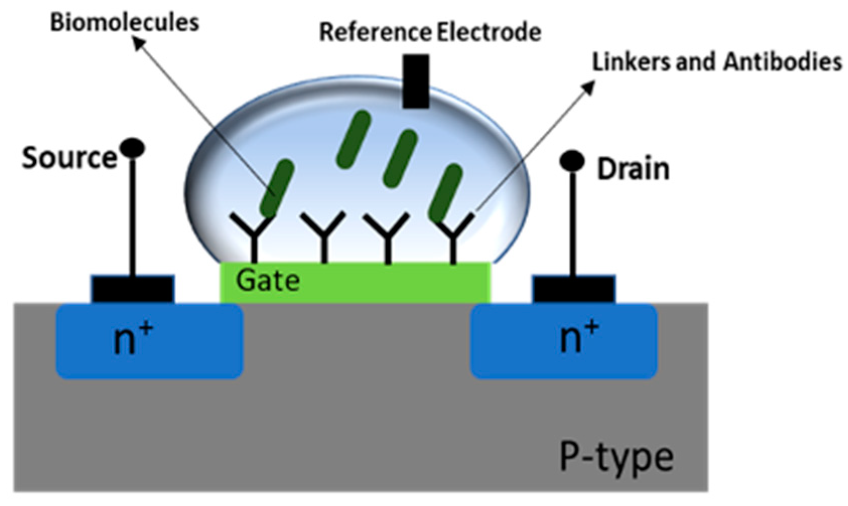
Figure 3.
Models of the electrical double layer at a positively charged surface: (a) the Helmholtz model; (b) the Gouy-Chapman model, and (c) the Stern model, showing inner Helmholtz plane (IHP) and outer Helmholtz plane (OHP) [27] Copyright Chemical Society Reviews, Royal Society of Chemistry.
Figure 3.
Models of the electrical double layer at a positively charged surface: (a) the Helmholtz model; (b) the Gouy-Chapman model, and (c) the Stern model, showing inner Helmholtz plane (IHP) and outer Helmholtz plane (OHP) [27] Copyright Chemical Society Reviews, Royal Society of Chemistry.

Figure 4.
Electrostatic effect of biomolecule (a) bulk materials (b) nanomaterials.
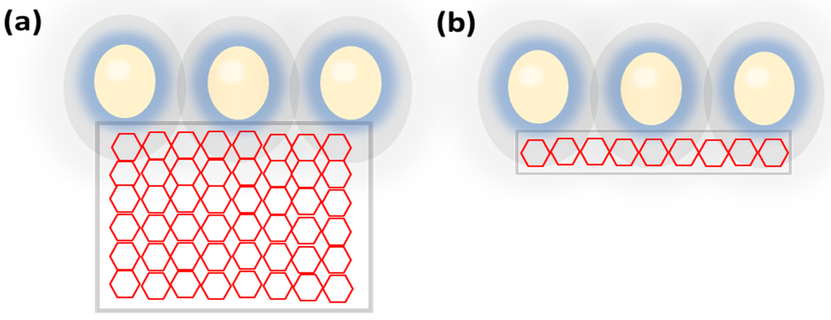
Figure 5.
(a) Molecular bond of the Graphene (b) Band gap of Graphene [59] Copyright (2014), with permission from applied sciences.
Figure 5.
(a) Molecular bond of the Graphene (b) Band gap of Graphene [59] Copyright (2014), with permission from applied sciences.
Figure 6.
Molecular structure and Bandgap of MoS2 [66] Copyright (2010), with permission from American Physical Society.
Figure 6.
Molecular structure and Bandgap of MoS2 [66] Copyright (2010), with permission from American Physical Society.

Figure 7.
(a) Graphene-based FET sensor for detecting the E-coli bacteria (b) ID-VLG curve of the FET before and after incubation of the E-coli bacteria; 100 CFU/mL. (c) ID-VLG of the bare graphene, linkers, anti E-coli, Ethanolamine, and tween20. (d) ID-VD characteristics at different concentration of the E-coli [80] Copyright (2011), with permission from ROYAL SOCIETY OF CHEMISTRY.
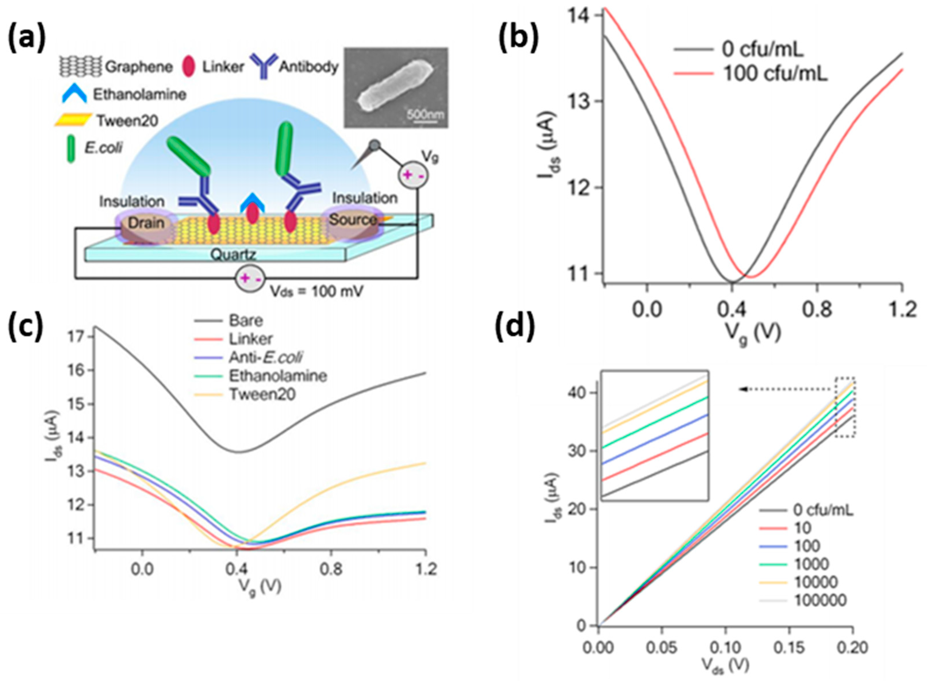
Figure 8.
(a) Schematic of MoS2 biosensor with HfO2 dielectric coating, bioreceptor, and biomolecules (b) Drain current (ID) versus gate voltage (VLG) of different pH values (c) ID-VLG profile of buffer and 100 fM streptavidin [38] Copyright (2014), with permission from American Chemical Society.
Figure 8.
(a) Schematic of MoS2 biosensor with HfO2 dielectric coating, bioreceptor, and biomolecules (b) Drain current (ID) versus gate voltage (VLG) of different pH values (c) ID-VLG profile of buffer and 100 fM streptavidin [38] Copyright (2014), with permission from American Chemical Society.
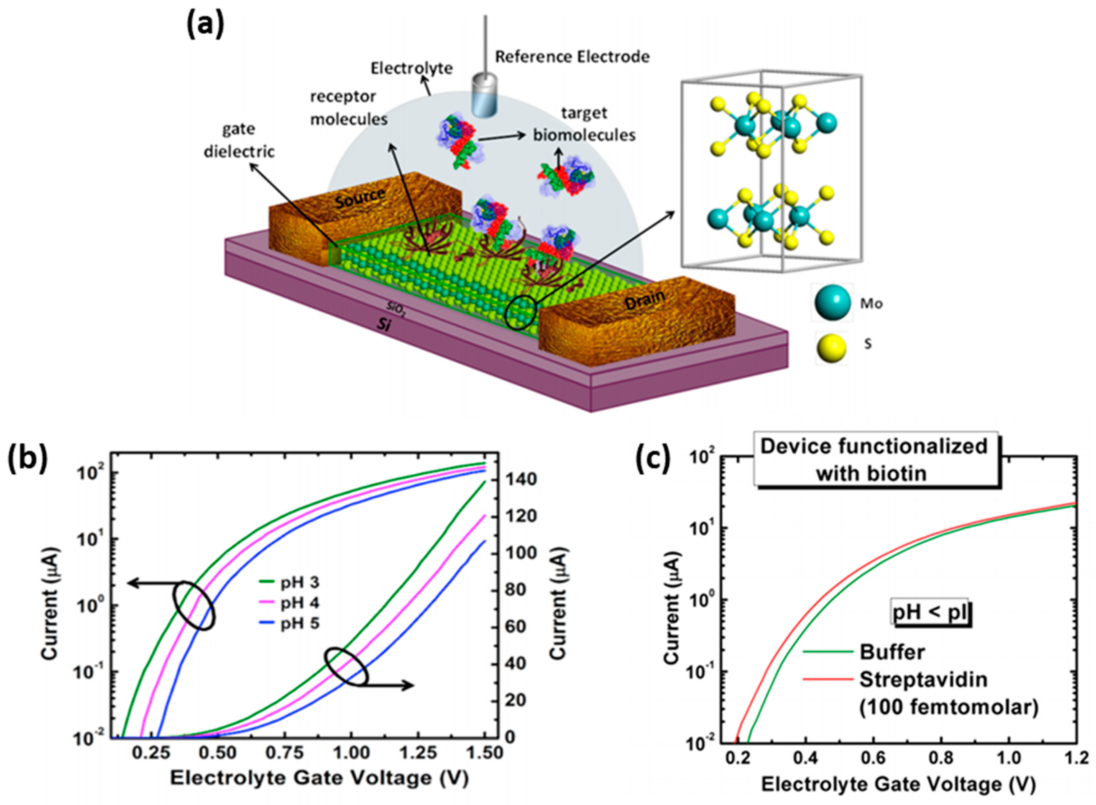
Figure 9.
(I) MoS2 device fabrication process (a) creating contacts via e-beam lithography on the top of supported MoS2 crystal (b) Etch SiO2 in Buffer Oxide Etch and (c) followed by ethanol washing and then critical point dryer is used to remove all wet contaminants (d) Final schematic. (II) Final device image of suspended MoS2 underneath the electrodes (a) optical microscope (b) SEM (c) AFM (d) AFM line profile [105]. Copyright (2013), with permission from AIP Publishing.
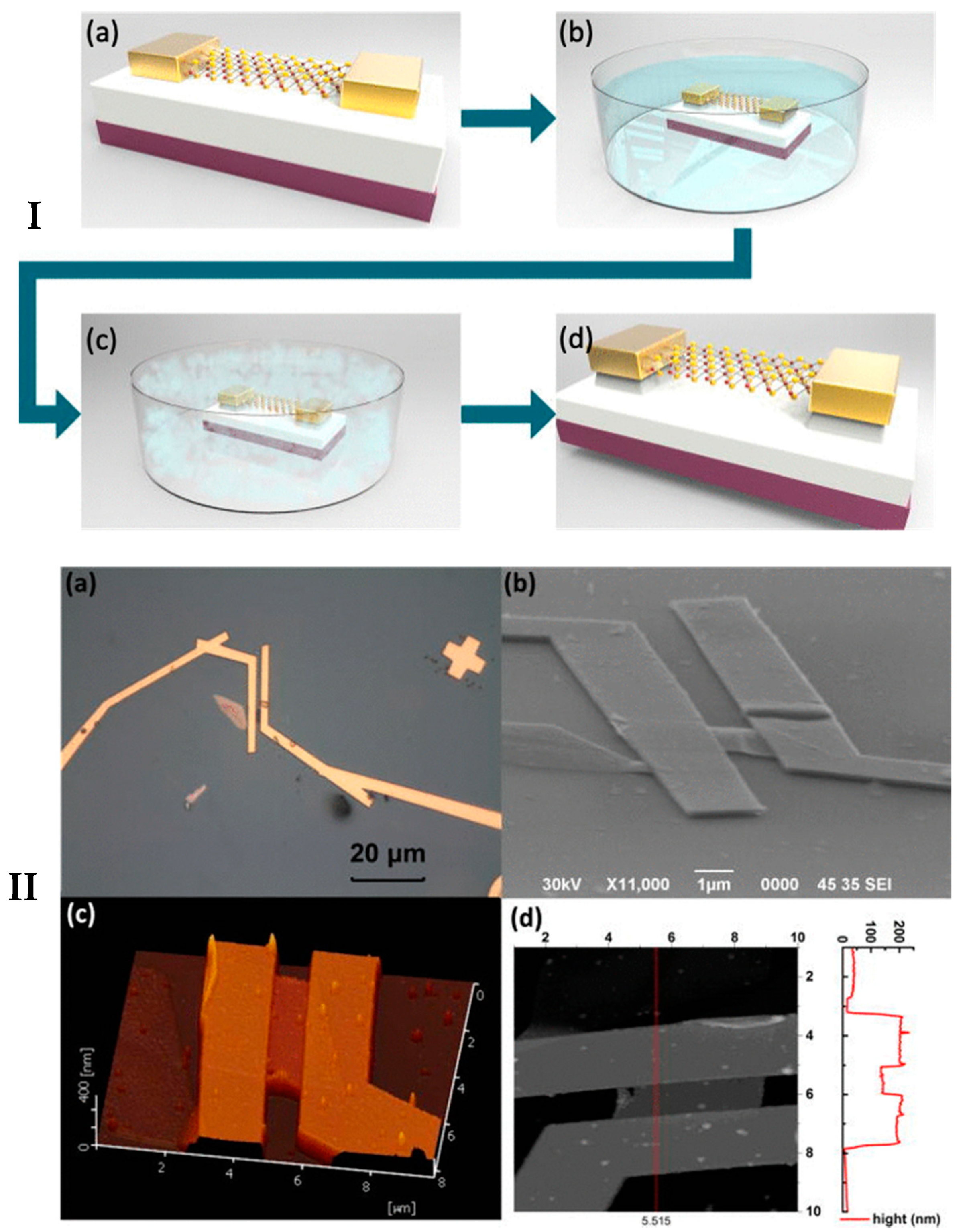
Figure 10.
(a) Schematic of Graphene FETs in the electrolyte solution (b) Conductance change of graphene while etching starts to drop gradually when HF introduced in the chamber (c) conductance vs. electrolyte gate voltage supported on SiO2 and suspended one. (d) conductance as a function of the electrolyte gate voltage in pH 6, 7, 8, and 9 solutions (e) Real time detection of solution pH [106] Copyright (2010), with permission from American Chemical Society.

Figure 11.
Ionic gating of suspended MoS2 device (a) Schematic and (b) optical image (c) SEM image of suspended device (d) I-V characteristics of different bias voltage (e) I-V transfer curve of suspended MoS2 at two different temperature [103] Copyright (2015), with permission from American Chemical Society.
© 2020 by the authors. Licensee MDPI, Basel, Switzerland. This article is an open access article distributed under the terms and conditions of the Creative Commons Attribution (CC BY) license (http://creativecommons.org/licenses/by/4.0/).
Share and Cite
MDPI and ACS Style
Masurkar, N.; Varma, S.; Mohana Reddy Arava, L. Supported and Suspended 2D Material-Based FET Biosensors. Electrochem 2020, 1, 260-277. https://doi.org/10.3390/electrochem1030017
AMA Style
Masurkar N, Varma S, Mohana Reddy Arava L. Supported and Suspended 2D Material-Based FET Biosensors. Electrochem. 2020; 1(3):260-277. https://doi.org/10.3390/electrochem1030017
Chicago/Turabian StyleMasurkar, Nirul, Sundeep Varma, and Leela Mohana Reddy Arava. 2020. "Supported and Suspended 2D Material-Based FET Biosensors" Electrochem 1, no. 3: 260-277. https://doi.org/10.3390/electrochem1030017