
Properties of Diamond-Based Neutron Detectors Operated in Harsh Environments


1
ENEA, Fusion and Technology for Nuclear Safety and Security Department, Via E. Fermi 45, I-00044 Frascati, Italy
2
Dipartimento di Ingegneria Industriale, Università di Roma “Tor Vergata”, Via del Politecnico 1, I-00133 Rome, Italy
*
Authors to whom correspondence should be addressed.
J. Nucl. Eng. 2021, 2(4), 422-470; https://doi.org/10.3390/jne2040032
Submission received: 17 August 2021
/
Revised: 13 October 2021
/
Accepted: 14 October 2021
/
Published: 28 October 2021
(This article belongs to the Special Issue Recent Advances in Applied Nuclear and Radiation Physics)
Abstract
:Diamond is widely studied and used for the detection of direct and indirect ionizing particles because of its many physical and electrical outstanding properties, which make this material very attractive as a fast-response, high-radiation-hardness and low-noise radiation detector. Diamond detectors are suited for detecting almost all types of ionizing radiation (e.g., neutrons, ions, UV, and X-ray) and are used in a wide range of applications including ones requiring the capability to withstand harsh environments (e.g., high temperature, high radiation fluxes, or strong chemical conditions). After reviewing the basic properties of the diamond detector and its working principle detailing the physics aspects, the paper discusses the diamond as a neutron detector and reviews its performances in harsh environments.
1. Introduction
Natural diamond is quite rare in nature and available at a high cost; despite this, its use for the detection of direct and indirect ionizing particles dates back to the early days of the nuclear age, e.g., around the beginning of the 1940s (1941) [1]. Indeed, the first solid state radiation detectors were made by natural diamond since, at that time, it was easier to find natural diamond crystals than to produce good quality silicon or other semiconductors [1]. The many outstanding properties of diamond [2,3,4,5] (see Table 1), which are going to be more thoroughly discussed in the following sections, justify the interest in this material as a radiation detector medium.
Natural diamond suitable for radiation detection must be of high electronic quality, that is, diamond with a very low content of impurities (such as nitrogen and boron at ppb levels) as well as minimal lattice defects. Defects and contaminants introduce spurious energy levels in the band structure, which can trap the carriers generated by the radiation (both electrons and holes), rendering the diamond not well-suited for radiation detection. High-quality natural diamond is rare and requires “ad hoc” selection and characterization of each sample and thus is costly.
Natural diamond exhibits four types: Ia, Ib, IIa, and IIb [3]. Detectors usually are realized using the type IIa natural diamond because it is almost free of nitrogen and transmits UV radiation better than other type of crystals; for instance, the type Ia has a large content of nitrogen atoms, of about 0.1%, in the form of small aggregates. Type IIb is free of nitrogen, but it is rich in boron impurities, which gives the crystal the typical bluish color, leading to a high electrical conductivity. Type IIb is very rare in natural diamond.
One of the earliest applications of natural diamond detectors was realized in Russia (a country rich in natural diamond) for detecting fast neutrons [6,7]. Other early studies of natural diamond properties and applications to neutron detection are reported in [8,9,10,11]. Application to high-resolution (~4% at FWHM) 14 MeV neutron spectrometry was reported in 1995 by Pillon et al. [12].
Despite their quite good performances, the use of natural diamond detectors was impractical, since large differences in the responses were observed due to a large variation in the impurities and defect levels. This limited the large-scale development and commercial availability of radiation detectors made with natural diamond. Example of natural diamond detectors sold by commercial companies can be found for medical applications [13,14,15,16,17,18], but today they have been replaced by synthetic diamond detectors.
Owing to the high cost and rarity of high-purity natural diamond, the interest quickly has moved toward the implementation of an artificial diamond detector medium. Moreover, natural diamond is available with geometries and dimensions not usually suitable for practical applications. This suggested the need to study and develop production techniques of artificial diamond to obtain a material showing performances compatible with device production requirements and with the possibility of modifying some specific properties simply by properly varying, in the right way, the growth process parameters. There are many different techniques to produce artificial diamond [19,20,21,22,23,24,25] of either the polycrystalline or homoepitaxial type. However, it is not in the scope of the present review to discuss them, except, shortly, in Section 2, regarding the technique of main interest for this work, namely the microwave plasma enhanced chemical vapor deposition technique (MWPECVD) [2,3,19]. Indeed, the use of artificial diamond in radiation detection has quickly grown after the year 1980 thanks to the development of the MWPECVD technique used for producing polycrystalline films (pCVD) first and, more recently (around the year 2000), high-quality homoepitaxial (monocrystalline or single crystal diamond (SCD)) films [26,27,28,29]. MWPECVD diamond can be produced, at least in principle, of the wanted electronic grade quality. Another parameter that can be controlled by the MWPECVD technique is the detector volume and mainly its thickness, which, as will be discussed in the next sections, dictates most of the properties of the diamond detector.
Historically, pCVD diamond was the first to be investigated as a detector medium [30]. The first tests were using radiation (e.g., alphas, electrons, and neutrons) as a probe to investigate the crystalline structure of the pCVD layer and obtain information about its quality, e.g., by measuring the collected charge (in this paper, the term “film” will be used to indicate diamond detector layers of up to few micron thickness, while the term “plate” will mean thickness of several tens of microns. We will make use of the term “layer” in all the cases in which the thickness is not defined or not important for the sake of the discussion). These studies demonstrated the suitability of diamond as a radiation detector. Detectors made with pCVD present some advantages (e.g., large area, low cost, easy production) and several drawbacks, the latter depending upon the application. Amongst the problems, let us mention the low energy resolution and the relatively low charge collection efficiency compared to SCD. These problems are due to the intrinsic defects in the polycrystalline structure (in-grain and boundary defects). Nevertheless, despite these problems, pCVD detectors fabricated at “Tor Vergata” University of Rome were, in collaboration with ENEA Frascati, first positively tested under long-lasting 14 MeV neutron irradiation [31] at the Frascati neutron generator in 2001 (FNG) [32] and then installed and successfully used at JET tokamak (in 2003) to detect the 14 MeV neutron emission from D-T thermonuclear plasma [33], during the JET trace tritium experiment. This was one of the earliest applications of artificial pCVD diamond detectors for fast neutron detection. Almost in the same time period, the first-ever produced artificial single crystal diamond neutron detectors were tested in Japan by Kaneko and co-workers [26,27] and at the NIF inertial fusion facility [34,35], as well as in the TRIGA reactor [36], always demonstrating their reliability and capability to withstand harsh environments while showing excellent, even when not unique and unprecedented, performances.
Together with these pioneer works, an extensive study and characterization of diamond (pCVD and SCD) as a detector material, mainly devoted to high-energy physics applications, was performed at CERN under the RD42 collaboration [37,38]. These studies covered almost all the physical and technological aspects related to the realization and use of diamond detectors for different types of radiation (p, d, n, π, e-, γ, etc.) including pioneer studies of pixel diamond detectors. Many and important improvements and knowledge of the physics and properties of artificial pCVD and SCD diamond have now been achieved thanks to the RD42 activities (see [39,40,41,42,43,44] and references therein, as well as the excellent review papers [45,46]).
Soon after the year 2000, the development and commercial availability of high-quality homoepitaxial diamond films (SCD) allowed for a quick and impressive improvement of the detection performances of diamond detectors, i.e., “100% charge collection efficiency and energy resolution <0.4%” [36,47], thus comparable to that of silicon (see Figure 1), and consequently paved the way for the application of diamond detectors in different research fields. The high-quality artificial diamond layers are usually referred to as “electronic grade” diamond.
Interesting results were reported for SCD detectors in UV and extreme UV detection for astrophysics and plasma physics [48,49,50,51,52], minimum ionizing particle detection in large accelerators [53,54,55], beam monitoring [56,57,58,59], X-ray and gamma-ray detection, for radiology and radiotherapy [60,61,62,63,64] and boron neutron capture therapy (BNCT) [65]. Diamond detectors were proposed and tested also as microdosimeters [66] and are now used in some therapeutic facilities [67]. Additionally, it was also found, by means of Monte Carlo simulation, that diamond detectors could reproduce the ambient dose equivalent (H*) [68] response to neutrons from a few MeV up to hundreds of MeV [69]; this could be useful in radiation dosimetry, where there is a lack of detectors able to measure dose in terms of ambient dose equivalent.
Though this work does not cover all the applications of diamond detectors, it provides an insight into the capability of diamond-based detectors to fulfill the many requirements needed to measure different types of radiation. This paper focuses mainly on diamond detectors for neutron detection and operation in harsh environments.
An ideal neutron detector should be compact, scarcely sensitive to gamma-rays but able to discriminate neutrons from gamma-rays, fast in the response and radiation, and temperature-hard. Additionally, it should be sensitive to both thermal and fast neutrons. While neutron detectors such as fission chambers, gas counters, scintillators, silicon detectors, etc., do not fulfill all these requirements, diamond detectors could represent a very good alternative for neutron detection (especially in harsh environments), since diamond meets almost all the above requirements [70]. On the other hand, diamond has a very low cross-section for thermal neutrons and is scarcely sensitive (via elastic scattering) to fast (<5–6 MeV) and low-energy neutrons. In contrast, for neutron energies higher than 5.7 MeV, it is considered a first choice thanks to the 12C(n,α0)9Be reaction, which produces a very sharp peak in the pulse height spectrum. This is one of the reasons for the interest in using diamond detectors in nuclear fusion research plants (tokamaks). As will be shown in Section 4.2, the sensitivity to thermal neutrons can be achieved using a thin layer of materials able to interact with thermal neutrons (6LiF [71,72], boron [65], and fissile isotopes [73,74]). Detectors based upon this principle (see Section 4.2) were developed and used in fission reactors, as well as applied in fusion tokamaks to measure neutron emission from D-D plasmas and the tritium production in a mock-up of the tritium breeding unit of ITER [72,75]. Additionally, in a “sandwich” configuration, a diamond detector with lithium or boron has been proposed for measuring in-core fast neutron spectra [76,77]. Thanks to the very fast response, diamond detectors were also proposed for time-of-flight measurements at CERN [78].
Last, but not least, we point out the intrinsic capability of diamond to discriminate the type of the impinging radiation such as charged particles from X-rays or gamma-rays. This is possible thanks to the shape of the electrical pulses produced inside the detector [79], which can be discriminated operating in pulse shape mode [80,81,82] (see Section 3.6).
The discussion above clearly shows the many reasons to study and use diamond-based detectors. It ought to be mentioned that one issue is with the difficulty of finding commercially available, reliable, and reproducible diamond detectors and/or diamond layers. Most of the studies and applications discussed in this work are based upon the implementation of custom-made diamond detectors, characterized by very different features, such as intrinsic properties, volumes, type of the electrical contacts, etc. This makes it difficult to compare data and results, and even the measurements are performed under similar experimental conditions. The lack of a good reproducible, commonly accepted procedure (mainly ascribed to commercial reasons) to produce artificial CVD diamond represents, the main reason limiting a more extensive use of diamond detectors. To this end, it is just mentioned here that the production of “electronic-grade” artificial diamond is of great interest to diamond-based electronics. Electronic devices based on diamond will show, among other things, great capability to dissipate the heat and thus high computing frequency and power well-superior to that of presently available silicon-based chips, whose physical limit has already been achieved [83].
This review paper deals mainly with the use of single-crystal diamond grown using the MWPECVD technique and operated in harsh environments. The paper first recalls (Section 2) the diamond-growing techniques and their properties. In Section 3, the diamond detector is first described and its properties discussed, pointing out the advantages and drawbacks of diamond. Emphasis will be given to studying the pulse formation inside the detector by discussing the fundamental Ramo-Shockley theorem in some detail. The transport of carriers in diamond will also be analyzed by discussing the mobility, the drift velocity, and the trapping and de-trapping properties of diamond. This is useful to understand the time behavior of the electrical pulse produced by a diamond. In Section 4, the neutron detection with diamond is discussed, reporting the n-Carbon interactions as well as the working principle of the lithium or boron film-covered detector. The basic aspects concerning the radiation hardness of diamond detectors are discussed in Section 5. In Section 6, a discussion about the behavior and the physics of diamond detectors operating at high temperature is also addressed. Finally, a brief discussion about open issues and possible further development is addressed in Section 7.
2. Diamond Growth and Properties
It is not in the scope of this review to discuss the methods for artificial diamond growth; however, since most of this paper is devoted to discussing the physics and the applications of diamond detectors produced by the MWPECVD technique, a short summary of this production method is addressed hereafter. More details of the various growing techniques are addressed in the literature, see, e.g., [19,20,21,22,23,24,25].
2.1. Diamond Production by MWPECVD Technique
The first point to consider when growing artificial diamond is that the stable phase of carbon is graphite, which has a planar sp2 hybridization. Diamond, in turn, results in the metastable allotropic form of carbon, and it is characterized by having a sp3 hybridization, which is a 3D configuration. Consequently, diamond atoms are arranged in a crystal structure (lattice) in which each carbon atom has four nearest neighbors in the typical tetrahedral arrangement, the so-called face-centered cubic lattice structure (Figure 2). There are eight atoms per unit cell, the nearest neighbor distance is b = 1.54 Å, and the unit cell dimension, at 298 K, is a = 3.567 Å (see Figure 2). There are 1.77 × 10²³ atoms/cm3; this is the highest atomic density of any material (in the earth). The diamond density, at 298 K, is 3.515 g/cm3 [2,3].
Like any metastable phase, diamond if strongly perturbed also gives way to the stable phase, that is, diamond can be transformed into graphite (but not the contrary); this can be attained in several ways, e.g., by heating diamond in an inert atmosphere; the onset of graphitization is detected at 1800 K. The rate of graphitization increases with temperature.
Diamond is also highly inert chemically, with two exceptions. At high temperatures, it is susceptible to oxidizing agents (e.g., oxygen, for T > 900 K), and it is subject to chemical bonding by some metals at high temperatures. This happens using carbide formers such as titanium, zirconium, tantalum, and tungsten. Nevertheless, at high temperature, there are also some metals acting as solvents for carbon, e.g., iron, cobalt, manganese, nickel, chromium, and platinum.
Natural diamond is formed under special conditions characterized by high temperature (1100–1300 K, [85,86]) and pressure (70–80 Kbar [87,88]). Similar conditions are used for producing the high-temperature, high-pressure (HTHP) artificial diamond, which results in very bad quality in terms of impurity content and crystallographic defects, thus not at all suited for radiation detection. Thanks to their low cost, HTHP diamond plates are used as a growing substrate when producing the MWPECVD diamond layers. Other artificial diamond production methods are based upon lower temperature and lower pressure compared to HTHP [85]. Amongst them, the MWPECVD technique is the most successful and is used for producing high-quality electronic-grade diamond. The main feature of the MWPECVD technique is that this process is performed at a lower temperature with respect to the temperature needed in other deposition processes (e.g., HTHP). This results in a significant improvement in the production of very high-purity diamond because the low temperature helps in limiting the impurities diffusion inside the deposition chamber.
Historically, the first attempts of diamond synthesis at low pressure are due to Russian research groups since 1963 [89,90], but the first heteroepitaxial growth of diamond on (001) silicon substrate was produced in Japan in 1992 [91].
The MWPECVD technique [2,3,19,92,93] is based upon the injection of microwaves from a magnetron inside the deposition chamber in order to dissociate the molecules of the CH4 gas needed for furnishing the carbon atoms. Typical reactors for plasma-enhanced CVD diamond growth are shown in Figure 3a,b, referring to the system used in the laboratories at ENEA C.R Frascati and at the Industrial Engineering Department of the “Tor Vergata” University of Rome. The proper gas mixture is typically composed by H2 and CH4. In general, the purity of H2 and CH4 gases is 99.9999%, and the gas mixture is 100 sccm H2 + 1–2 sccm CH4. Both gases flow through the deposition chamber made of quartz or a stainless-steel tube, which is placed across a waveguide connected to a commercial microwaves (MW) generator and acts as a resonant cavity. On the bottom of the chamber, a substrate is placed on a sample holder that is properly connected to a water-cooling system. When gases reach the zone where microwaves are present, the molecules forming the gas adsorb energy and are broken into active radicals so that a stable plasma burns at the center of the deposition chamber, coupling to the substrate on which the deposition process takes place. The temperature of the growing film is monitored in real time by means of an infrared optical pyrometer. This process requires well-defined thermodynamic conditions that, if not satisfied, lead to a mismatch in the lattice structure between the monocrystalline HTHP substrate and the growing diamond, resulting in polycrystalline growth. If the substrate is made of silicon, polycrystalline diamond can be grown instead. In this case, to activate the growing process, the Si crystal surface must be properly prepared for nucleation via an “ad hoc” surface treatment (seeding) [85,92]. It might be stressed that hydrogen is fundamental during the growth of diamond because it reacts with dangling bonds on the surface of diamond that must be terminated. H atoms terminate surface states on diamond, leading to a stable sp3 lattice. H, in turn, is removed by hydrocarbon radicals that can leave C atoms on the surface. In fact, another important property of hydrogen is that it forms radicals with CH4 (e.g., CH3) that are very important for the whole process [85]. The as-grown CVD diamond presents a surface termination of hydrogen bonds. It is known that a hydrogenated surface gives rise to high p-type surface conductivity, whereas oxygen termination of surface bonds results in an insulating surface. Oxygen-terminated surfaces can be obtained by a wide range of treatments such as thermal annealing in air, boiling acid treatments, oxygen plasma, and ozone atmosphere. Growth parameter optimization was investigated, allowing for producing CVD diamond of excellent quality as the material for detectors’ realization [94].
Several application fields of diamond including radiation detection require flattened and polished diamond surfaces. Due to the extreme hardness of diamond, the polishing procedures of diamond are demanding. Many polishing techniques were developed to obtain a smooth and flat diamond surface such as mechanical polishing, thermochemical polishing, laser polishing, and ion beam polishing in reactive ion etching (RIE). Each of these methods shows different characteristics, such as the high capability to remove material, the ability to obtain high-quality polished surfaces, and low processing costs. The selection of the polishing technique depends on the practical application. Regarding diamond detectors fabrication, mechanical polishing is generally employed before deposition of metallic contacts.
2.2. Diamond Properties
Diamond as silicon (Si) and germanium (Ge) stands on the IV-A group of the periodic table of elements, thus sharing with these elements the property of being a semiconductor. Semiconductors have crystalline lattice with allowed energy bands for electrons, the so-called valence and conduction bands, respectively (Figure 4), separated by an energy gap Eg. At room temperature, electrons stay in the valence band where they are bound in the outer atomic shells of the carbon atoms forming the lattice. Under some circumstances (e.g., under supply of external energy such as increase in temperature, radiation etc.), electrons can jump to the conduction band. A vacancy (or hole, h) is thus produced in the valence band, and we talk about the formation of e/h pairs (EHP). The probability, per unit time, to promote an electron to the conduction band depends upon the absolute temperature T:
where KB is the Boltzmann constant, Eg is the band gap in eV, and S is a constant depending upon the material. Eg is typical of each semiconductor and most of the semiconductor’s properties are depending upon its magnitude. At room temperature, diamond presents a band gap Eg = (5.470 ± 0.05) eV [95], while Si has a gap of 1.11 eV and Ge has a gap of 0.66 eV. In the presence of an external electric field, the EHPs produced by the temperature (Equation (1)) generate a current usually referred to as “dark current”. Using Equation (1), we can easily see why, e.g., at room temperature, the dark current of diamond detectors is much lower than that of other semiconductors detectors with a smaller Eg. The Eg values explain why, e.g., a Ge detector needs to be cooled at room temperature while silicon and diamond do not. This is of fundamental importance for radiation detection, since it implies a much higher signal to noise ratio in favor of the diamond detector with respect to the silicon detector. As a consequence of the low dark current, diamond also presents a high resistivity (>1013 Ω·cm), a very important property for a detector (Section 3).
Diamond also shows very interesting optical properties. It is practically transparent to the optical radiation, from the far infrared to the ultraviolet, corresponding to the gap at ~225 nm (5.47 eV). Weak transitions at two or three phonons in the 1332–2664 and 2665–3994 cm−1 intervals are observed, which represent the only regions of intrinsic absorption. Other types of absorptions must be attributed to the impurities [95]. These optimal transparency characteristics, together with its mechanical resistance, make diamond an ideal material for the production of optical windows for power lasers or to optically connect harsh environments [19]. A sharp cut of the detector responsivity is observed for photons with wavelength >220 nm, rendering diamond well-suited to UV detection.
Diamond exhibits many other outstanding properties (Table 1); amongst them, let us mention the high carrier mobility (the highest for holes, 2280 cm2/Vs at room temperature [95]), which, in turn, permits high-speed and high-count-rate capability. Other relevant properties are high break-down field (>107 V/cm), low relative dielectric constant ε (ε = 5.7, which reflects its low capacitance and hence renders diamond a potential source of high-speed and low-noise electronic devices), and high fusion temperature (4100 °C). The latter coupled to the highest thermal conductivity (20 Wcm−1 K−1) and the large Eg render diamond suited for operation at high temperature. For the sake of radiation detection, it worth also mentioning the good radiation hardness [96,97,98,99,100,101], which is related not only to Eg but also to the high dislocation energy (Ed) of carbon atoms in diamond (Ed = 43.3 eV) [84], which, in turn, depends on the high bonding energy of the carbon atoms hosted in the typical cubic-centered lattice structure. All together, these properties render diamond unique, making feasible the realization of fast and low-noise radiation detectors suited for withstanding harsh environments [3].
Carbon also has a low atomic number (Z = 6) close to that of human tissue and a near constant ratio of stopping power with water for proton and carbon ions. This fact renders diamond interesting for radiation dosimetry and microdosimetry [18,65,66,67,102,103,104,105,106,107,108,109,110,111]. The low Z also renders diamond scarcely sensitive to gamma radiation. This could be helpful when operating in mixed neutron-gamma fields to enhance and/or separate the neutron response. Therefore, low Z means reduction of the stopping power, which results in a reduction of the sensitivity of the detector to ions and gamma-rays.
3. The Diamond Detector
A typical diamond detector, in its simpler form, is a two-terminals device formed by an intrinsic diamond layer sandwiched between two metal contacts (Figure 5). The high specific resistivity of diamond (>1013 Ω·cm) allows for a very simple construction of the detector, which renders the diamond detector a “solid state ionization chamber”.
A biasing voltage (HV) is applied between the two electrodes, typically of the order of 0.5–2 V/μm. Too-high HV can affect the detector response (Section 3.2 and Section 3.3). Different metals can be used to deposit the contacts (the so-called metallization procedure, see Werner [112]), the most common being Al, Cr, Ti, Ni, Ag, Au, Pt, and W. Typical metal layer thickness is in the range 30 ÷ 200 nm. Often, two (or even three) layers of different metals are used to form a layered metal electrical contact (e.g., Ti/Pt/Au, Cr/Au, etc.). In this case, the thinner metal layer is deposited directly on top of the diamond surface, while the thicker one is on top of the first metal layer; the latter is used to avoid the oxidation of the first one (e.g., Cr/Au) or to improve the mechanical and/or thermal properties and also detector bonding/contacting.
Depending upon the metallization procedure, the metal–diamond junction can form either Schottky or ohmic contacts. The former is usually formed when a metal layer is just deposited at room temperature (either by sputtering or evaporation technique) on top of a diamond surface. In this case, a rectifying junction characterized by a typical electrical potential (Schottky barrier) is obtained. The magnitude of the barrier (typically 0.5 eV ÷ 1 eV) depends upon the used metal, since it is due to the difference in between the metal and diamond work functions (Table 2, [113]). When metal and diamond are brought into contact, electrons flow from the material with the lower work function to the material with the higher work function. As a consequence, one side becomes slightly positively charged, and the other slightly negatively charged, forming a junction at the metal–diamond interface with physical dimensions of a few atomic layers. For a detailed analysis of the Schottky barrier properties, see [113,114,115,116,117,118]. It ought to be stressed that some metals (e.g., Ag) keep the rectifying properties up to a temperature of about 800–900 °C, and these high-temperature diodes are studied for application other than radiation detection (e.g., electronics devices for avionic engines where the operational temperature is several hundred degree Celsius (see, e.g., [119])).
In order to obtain an ohmic contact, the diamond sample must be annealed. During the annealing, some metals (e.g., Al, Ti, Cr) react with the diamond and form carbides [119,120,121], resulting in a final ohmic contact. Annealing time and temperature depend on the type of metal. This technique dates back more than three decades [122]. A very thin layer (1–3 nm) of a so-called diamond-like carbon (DLC) structure is formed at the interface between the diamond and the metal, which is assumed to improve the electrical properties of the detector. DLC is a form of amorphous carbon between diamond and graphite, containing a significant portion of sp3 bonded atoms in the matrix. DLC films can also be grown when carbon is deposited under energetic (~10–100 eV) bombardment, where the instantaneous local high temperature and pressure induce a portion of carbon atoms to bond as diamond [121]. This layer allows for the injection of both holes and electrons in the diamond substrate. Additionally, the DLC layer becomes a seed for the sputter deposition of high work function noble metals (Pt, Au), which allows metals to cohere to the diamond surface. As platinum and gold have a higher work function than diamond, this permits electrons present at the diamond surface to be driven toward the noble metals via quantum mechanical tunnelling through the thin DLC layer acting as a quantum mechanical tunnelling junction. Another notable procedure used to create ohmic contacts on diamond is called graphitization. This method involves treating the surface of the diamond with a high-power UV laser, creating a thin layer of graphite with quite low resistivity.
Ohmic contacts must have low resistivity, good adhesion, high thermal stability, high corrosion resistance, bondable top-layer, and suitability for micro-patterning [112]. All these properties, except the first, also apply to Schottky contacts, which, instead, must have high resistivity.
There is another method to obtain ohmic contacts, which is based upon the deposition, through the MWPECVD technique, of a layer of SCD diamond highly doped in boron (concentration about 0.5 × 1020 cm−3) on top of an intrinsic SCD film. This technique was first proposed by K.L. Moazed and co-workers [122] in 1988 and soon after used and studied and further developed by others [123,124].
The metallic contacts must ensure a uniform electric field inside the bulk of the diamond radiation detector, when a bias voltage is applied, in order to efficiently collect the charges at the electrodes. If the contacts on both diamond surfaces are ohmic, the current across the junction depends linearly on the applied voltage. On the other hand, the use of Schottky contacts has the merit of low dark current due to the metal/semiconductor barrier height and high response speed. This is very useful for several applications such as Time-Of-Flight (TOF) measurements, extreme-UV and soft X-ray detection, and dosimetry.
Detectors having on one side boron ohmic contact and on the other side a standard metal–carbon Schottky contact are routinely produced at “Tor Vergata” University of Rome and used for different applications. The properties of such a detector, also named a “layered” diamond detector (LDD), are detailed, addressed in [125]. LDDs covered with a thin 6LiF layer were used for neutron detection [36]. However, LDDs are particularly suited for X-ray and UV detection as well as dosimetry [52,58,65,66,67,69,71]. This is mainly due to the built-in potential due to the Schottky barrier, which allows the use of the detector without the need for any external bias, a not-negligible point for detectors exposed to intense radiation fields, e.g., in radiotherapy (a version of this detector called Microdiamond is commercialized by PTW-Freiburg GmbH company for medical physical applications [17]). These detectors resulted well performing at high temperature [126].
From the literature [112,113], we are aware of important issues related to the technology of electrical contacts’ deposition on diamond. These issues need to be solved to allow a reliable operation of these devices, especially in a harsh environment. Among them, let us mention:
- Metallization. Conventional or inadequate contact fabrication may result in poor mechanical adhesion, polarization effects, and unrepeatable results.
- Mechanical adhesion. The mechanical adhesion of the metal electrode on the diamond surface. A flat, smooth surface (diamond film is polished before use) may presents few adhesion points, and a metal thermally evaporated on diamond may not adhere completely. The metal could peel off (after some operational time), and the electrical signal could deteriorate, reducing the device lifetime and stability. The peeling was observed in a previous study [110].
- Polarization effects. Polarization phenomena occur when electric currents pass through diamond and the electrical contact is not able to extract and/or inject carriers fast enough. The detector loses its stability because charge accumulation occurs within the crystal. The trapped carriers establish an electric field that is opposite to the field produced by the external bias. This point is very important for reliable long-lasting operation as well for operation in harsh environments. Polarization is observed after strong irradiation [127] as well as at high temperature (T > 220–240 °C, [128]). Polarization will be further discussed in Section 3.8.
A straightforward approach to studying the performances of electrical contacts before exposure to radiation is the measurements of the I-V characteristics versus biasing voltage. As an example, Figure 6a shows the typical I-V curve for a 500 μm thick detector fabricated with two Schottky metal contacts (Pt-Pt), to note the typical (double) diode shape. Figure 6b shows typical ohmic I-V characteristics measured for a 500 μm thick diamond detector with Ag-Ag contacts post deposition annealed in vacuum at 600 °C. The I-V curves for the “layered” detector (boron doped/intrinsic diamond/Al), shown in Figure 6c, exhibit the typical (rectifying) Schottky diode curve.
3.1. Charge Carriers
In the following, we will use the word “carrier” to mean electrons (e) and/or holes (h). It worth distinguishing how these carriers are generated. Carriers generated by thermal effects are, hereafter, called “free carriers”, while carriers generated by not-thermal energy (e.g., by radiation) are called “excess carriers”. In both cases, electron–hole pairs (EHP) are generated.
The production rate of the free carriers is given by Equation (1) and depends on Eg and (absolute) temperature. The production rate of the excess carriers depends upon the intensity of the absorbed radiation (per unit volume or mass), divided by the energy εp to produce one EHP. According to Klein [129] εp also depends upon the type and energy of the impinging radiation, and usually it is of the order of a few eV. In [30], a detailed discussion about the evaluation of εp is reported, while a model to calculate εp was proposed by Shockley [130]. For diamond, Canali et al. [11] reported εp = 13 eV (e.g., εp = 3.62 eV for Si). Since the εp value for diamond is higher than for silicon, we should expect diamond electrical signals to be smaller in magnitude than for silicon and to also have lower energy resolution (FWHM). This because the amplitude is proportional to the number NEHP of EHP while the FWHM is proportional to the inverse square root of NEHP.
In the case of charged particles, the ions moving throughout the diamond generate a high density of EHP along their tracks (which are typically straight lines). In the case of mono-energetic ions with a kinetic energy of up to several MeV, the track-length is in the range from a few up to tens of μm (e.g., the range in diamond of 5.5 MeV alphas from 241Am is ~14 μm). As known, ions lose energy according to the Bragg curve, which peaks at the end of the ion range, so most of the EHP are formed there. A sharp peak is thus produced in the pulse height spectrum (PHS), well-described by an (almost) Gaussian distribution centered around the so-called peak centroid. The position of the peak centroid is a measure of the average energy deposited by the monoenergetic ion in the material, which, in turn, is proportional to the ion energy. This allows obtaining a linear relationship between the deposited energy and the position of the peak centroid in the PHS. This is fundamental for the application of diamond detectors in radiation detection and mainly for dosimetry and spectrometry [11,131].
3.2. Mobility and Drift Velocity
Similarly to any other semiconductor, the transport of carriers in diamond can be discussed using known concepts and quantities (e.g., drift velocity, drift time, mobility of carriers, etc.). Let us consider an ideal diamond detector as that pictured in Figure 5 with one excess charge carrier moving across it. L is the distance between the two electrodes, and E (V/μm) the external electrical field applied to the detector (see Figure 5). Let us call td the time needed to a carrier to cross the thickness L (μm) (td is the transit or drift time); thus, we can define the drift velocity vd of the carrier as vd = L/td. Therefore, the charged carrier is moving because of the external electrical field E, and in between two collisions, the carrier is subjected only to E, and it is moving in a straight line; thus, its drift velocity depends upon E:
where μ (μm2/V·s) is the carrier mobility, which, in turn, is defined as:
In Equation (3), m* is the effective mass of the carriers and τR is the relaxation time, i.e., the time in between two collisions of the carrier with the atoms of the lattice, which brings the electrons in thermal equilibrium with the lattice, thus becoming temperature-dependent. Let us note that the definition for μ relates vd to intrinsic physical parameters of the diamond crystal.
According to Equation (2), the carriers drift velocity vd increases with the electrical field. This increase is found not to be linear versus E, as it could resemble from Equation (2) but, according to Li and Kraner [132], for E higher than 1.4 ÷ 1.5 V/μm [45], in diamond, vd tends to saturate up to reaching the saturation drift velocity (vds). The drift velocity versus the electric field can be written as [132,133]:
where μ0 is the low field mobility of carriers (for E < 0.1 V/μm). Fitting the data of the measured vd versus E by using Equation (4), Pernegger derived the saturation drift velocity for electrons (vdse = 9.6 × 106 cm/s) and holes (vdsh = 1.4 × 107 cm/s) [134], respectively, at room temperature. The measure of vd was performed by using the transient current technique (TCT) [135,136]. Let us note that the mentioned saturation values for E are just above those typically used for operating diamond (and semiconductor) detectors (E ≤ 1 V/μm). For low electrical field value (E < 0.1 V/μm), the drift velocities of electrons and holes tends to be the same [134]. A plot of Equation (4) is shown in Figure 7. The saturation of the drift velocity leads to the experimentally observed saturation of the charge collection efficiency (CCE) with E. CCE is the fraction of produced excess carriers, which is collected at the electrodes (see Section 3.4).
Concerning the mobility, by mixing Equations (2) and (4), we obtain:
This is the so-called effective mobility; Equation (5) is also plotted in Figure 7. Equation (5) is valid in the same range for E where Equation (4) applies. According to Equation (5), the charge carrier mobility is highest at low E field strength and gradually decreases as E increases, as found experimentally by Pernegger (see Figure 4b in [134]). Let us note that, for diamond, the mobility for holes is the highest amongst the semiconductors. Pernegger, fitting the experimental data of the measured vd in the range 0.2 V/μm < E < 1.5 V/μm (which is the range for E where the drift velocity approaches the saturation velocity), reported values of μ0e = 1714 cm2/Vs and μ0h = 2064 cm2/Vs for electrons and holes mobility, respectively, at room temperature. μ0e and μ0h are the so-called low field mobility, that is, the mobility for E < 0.1 V/μm. The reduction of the carrier’s mobility versus the electrical field is generally observed in semiconductors.
The saturation of the drift velocity is attributed to the fact that the main dominant scattering mechanism for carriers in diamond is associated to optical phonons. Therefore, parameters such as the optical-phonon energy (temperature-dependent), the carriers’ (electrons and holes) density, and their trapping times must be considered to understand the mobility saturation phenomenon. Furthermore, when operating a detector in the region of low field mobility, μ is independent of E. In this case, the current flows according to the Ohm law. At high electrical field, the scattering process becomes dominant so that the average kinetic energy of the carriers does not increase. This leads the drift velocity (vd) to be independent from E and thus μ 1/E (see Equation (5)).
Other values for the mobility of holes and electrons in diamond are available in the literature [96,137,138]. For example, according to Jansen [96], at 295 K, the low field electron mobility is μ0e = 1440 cm2/Vs, and, as for the Pernegger data, it is lower than the hole mobility (μ0h = 2280 cm2/Vs). References [96,138] reported a range of measured mobility data, e.g., at room temperature, the electrons’ mobility (3500 < μ0h < 4500 cm2/Vs) was generally higher than the hole mobility (2600 < μ0e < 3800 cm2/Vs). The observed differences could be ascribed to the different type/quality of diamond crystals used as well as to different experimental conditions.
3.3. Temperature Effects on Mobility
According to the literature, the carrier’s mobility is temperature-dependent and decreases as the temperature increases [96,137,138,139,140,141]. This is a common feature of semiconductors [142], and it is very important for detectors (e.g., diamond) to be operated at high temperature since the carrier’s transport properties (including scattering) are influenced by mobility (see Section 3.2).
It is known that the atoms forming the lattice are vibrating, the amplitude of the vibration depends upon the temperature, and this vibration is distorting the (periodic) lattice structure. The vibration energy is quantized (phonon) [142]. The phonon interacts with carriers by scattering. Two types of phonons are considered, “optical” and “acoustic”, respectively, which differentiate for the frequency and thus the energy. The interaction with acoustic phonons is considered the dominant scattering mechanism for carriers in diamond. Each one of the scattering mechanisms mentioned above is temperature dependent. We can describe the effect of the j-th scattering process by assuming that the carriers have a mobility μj. Following the Mattiessen rule [141,142], the effective mobility can be written as:
The already mentioned decrease in mobility with the temperature can be demonstrated by a heuristic approach based upon basic quantum physics concepts. Let us consider the phonon scattering, the scattering rate R0 is proportional to temperature (kT) and to the density of states nD. If the carriers averaged kinetic energy is Ec the density of states nD (Ec)1/2 and hence to (kT)1/2 [142]. Therefore, the relaxation time τR is temperature-dependent:
Recalling Equation (3), which links the relaxation time τR to the carrier’s mobility, we obtain the temperature dependence of mobility due to phonon scattering:
The result above is confirmed for holes by the experimental observation of Isberg and co-workers for the temperature range 150 ÷ 350 K [138]. At higher temperatures and up to around 550 K, still in [138], a steeper decrease in μ versus T is reported (~T−3.4).
For the sake of the operation of diamond detectors at a high temperature (Section 4.3) let us complete this discussion by mentioning that the carriers can also interact with the imperfection of the lattices (e.g., vacancy, chemical imperfections, etc.). These imperfections alter the regular structure of the lattice and hence the flowing of the carriers in the crystal. The scattering between the carrier and the charge of the defects is of the Coulomb type. In the case the carrier’s density is high (>1018 cm−3), carrier–carrier scattering, which is a Coulomb interaction, can also be possible.
3.4. Charge Collection Efficiency
In an ideal detector, the number NEHP of excess carrier pairs generated by a ion of energy EIon is NEHP = EIon/εp. These carriers, as will be discussed in Section 3.5, induce a prompt current and are collected at the electrodes after drifting under an external electrical field E applied to the detector. Therefore, in practice, some traps and/or recombination-sites (due to crystal defects and/or impurities) are present in the diamond film, so not all the produced EHP are actually collected at the electrodes, because some are trapped by these traps. The ratio between the collected charge (Qc) and the produced one (Q0) is called charge collection efficiency (CCE or η):
The CCE is a very important parameter useful to understand most of the electronics properties of the diamond detector. Let us consider the case of a minimum ionizing particle [143] passing through a diamond detector of thickness L. A minimum ionizing particle (MIP) is a particle whose mean energy loss rate through matter is close to the minimum (e.g., relativistic particles such as cosmic-ray, muons, electrons, etc., are minimum ionizing particles). A MIP produces 36 EHP per micron of diamond [30]. Let us call this quantity . The charge produced by a MIP in the distance L is thus Q0 = q0L. This is the maximum total charge we can expect to be produced. In the case of the largely used 5.5 MeV alpha from 241Am whose range in diamond is ~14 μm, it produces 4.2 × 10⁵ EHP in total (thus 2.8 × 10⁴ EHP/μm), resulting in Q0 = 8.1 × 10⁻¹⁴ C. However, it could happen that after moving for a distance dT < L, called the charge-collection distance (ccd), the charges are trapped inside the detector. In this case, the collected charge QC is:
Thus, we obtain:
Therefore, by measuring QC, we can obtain the ccd. A method for measuring the ccd for diamond detectors is discussed in [144].
The increase in the ccd represented one of the main goals (especially for pCVD), since the ccd is directly correlated to the diamond film quality (number of impurities and defects). Indeed, the ccd (and CCE) depends upon some intrinsic physical parameters (e.g., carrier’s mobility) of diamond; we are going to discuss this hereafter.
Let us consider again Equation (11). It is possible to introduce the ccd by considering an excess carrier moving under the effect of the external electrical field. As discussed in Section 3.2, the distance the charge carrier can travel depends upon its drift velocity vd and drift time td; this distance is named the collection distance (λc):
Equation (12) is another way to define the ccd since it holds both for electrons and holes. The ccd thus depends upon both carriers:
Equation (13) is interesting because it shows that the collected charge Qc (hence CCE) is inversely dependent from the diamond film thickness L. We will see in the next sections that most of the properties of diamond detectors are depending upon 1/L. Equation (13) also shows that we can define a collection distance for each carrier (λce and λch, respectively), furthermore pointing out a relationship between E and the ccd, which, accounting for Equation (5), is not linear. This is experimentally observed. Considering the temperature dependence of mobility, we can conclude that the ccd is a function of both E and T.
The discussion above refers to an “ideal ” detector where no trap centers are present. In a real situation, traps of different types are present in the crystal that capture both e and h. In this case, the ccd cannot be expressed by Equation (13); therefore, it is possible to re-write Equation (13) to account for the contribution of these traps by using the Hecht equation [145,146]. The Hecht equation considers the fact that the free carriers, once trapped, stay in the traps for a time characteristic of each trap type called the trap lifetime, after which they are released. Therefore, a carrier before trapping will leave in diamond for a time τ called the carrier lifetime (τe for electrons and τh for holes). The use of the Hecht equation leads to the following expression for the CCE (all the quantities involved in the equation where already defined; z is the distance of the free carrier from the electrode where it is collected, see Figure 5):
When testing a diamond detector, the first step is to determine the external voltage (HV), e.g., by using an 241Am alpha source, which emits alpha particles of 5.5 MeV. In this case, locating the 241Am alpha source close to one of the electrodes, e.g., the one at positive potential, a typical result is that the peak centroid of the alphas pulse height spectrum (PHS) moves toward higher values as E increases (i.e., increase in the HV). The peak shifting is observed until it reaches a saturating value for the E (HV), above which the peak position is scarcely sensitive to its further increase (Figure 8).
3.5. Charge Induction and the Ramo-Shockley Theorem
To understand the mechanism of pulse generation in diamond detectors (as well as for any semiconductor), we shall consider the Ramo-Shockley theorem [147,148]. We consider a diamond detector made by a diamond layer sandwiched between two metal electrical contacts and, e.g., a charge particle interacting in position z, thus producing EHP (Figure 5). Under the effect of an external electric field E, the excess charges move away from each other. During the drifting, charges can be either trapped by the traps present in the diamond or move toward the electrodes until they reach them. Electrons will move toward the positive electrode (anode) while the holes will move toward the negative electrode (cathode), the latter usually kept at the ground potential.
It is pointed out that it is not necessary for the free charge carriers to actually reach the electrodes to generate the electrical current measured by the external circuit to which the detector is connected since the Ramo-Shockley theorem applies. The free carriers couple to electrodes and induce, instantaneously, mirror charges. The drifting charges, if not trapped, will reach the electrodes after a delay time depending upon their initial position, thus contributing to the pulse timing, which also depends upon the drift velocity vd. Since, in diamond, both holes and electrons have very high mobility (Section 3.2), we should expect a fast collection time and hence a fast pulse rising time. It worth noting that no delay time is observed in between the EHP production and the rising of the electrical signal; this is an empirical demonstration that the Ramo-Shockley theorem is valid for the diamond detector. To calculate the instantaneous current let us consider again the diamond detector reported in Figure 5.
Let us call L the thickness of the detector and V0 the biasing potential applied to the detector; E0 = V0/L the constant electric field. As demonstrated independently by Ramo and Shockley [147,148,149], the instantaneous current on a given electrode induced by a moving point charge q at position z in the inter-electrode region (Figure 5) is given by:
vd being the instantaneous drift velocity. The induced charge is:
In Equations (15) and (16), Ew and φw are the so-called weighting electric field and weighting potential, respectively. Ew and φw are the electric field and potential that are present at the charge’s (instantaneous) position z if the following three conditions are verified: (a) the voltage of the electrode for which the induced charge is to be calculated is set to 1 V; (b) the voltage of all the other electrodes are set equal to zero; (c) all other charges are removed (no space charge). Let us note that these three boundary conditions are to be applied to the Laplace equation for the geometry under study (ρ0 and ε0 being the charge density and dielectric constant, respectively, and φ the electrical potential). In the case that no space charge is present, the Laplace equation reduces to the Poisson’s equation . The latter is the basic condition for which the Ramo-Shockley theorem was first demonstrated. The applicability of the Ramo-Shockley theorem in the presence of space charge was later on demonstrated by Cavallari [150]; this result is fundamental for application to diamond detectors since space charge is often present in diamond detectors (see Section 3.8).
According to their definition, both Ew(z) and φw(z) are not the actual electrical field and potential in the detector; they are rather an artifice useful for calculating the induced current (or charge). From Equation (16), once φw(z) is known, the induced charge on the electrode of interest can be calculated simply by taking its differences in between the starting point (z1) and the end point (z2) of the moving charge. The path z(t) (as well as the drift velocity vd) of the moving charge must be calculated from the actual external electrical field E0. Let us note that the use of φw(z) is possible because the induced charge does not depend upon the drift velocity vd of the moving particles (thus the assumption of the first hypothesis, ΔV = 1 V). vd depends upon the actual electrical field (see Equation (5)) and not on the weighting electric field [151]. This relates to the image method, which is at the basis of the Ramo-Shockley theorem. The hypothesis (b) above relates, in turn, to the superposition principle for both the potential and the electrical field. If several electrodes are present (e.g., pixel detector) the calculation, e.g., for φw, is performed for each j-th electrode, and thus the corresponding induced current is calculated as already explained. The procedure is repeated for all the electrodes, and the final total induced current is the algebraic sum of all the calculated currents. It is obvious to state that if the position z(t) of the charge q is known as function of time t, the induced charge, Q(t), is known too. This allows obtaining the shape of the output pulse from the detector.
For a planar configuration made by two large parallel electrodes separated by a distance L (in the z direction, Figure 9), it can easily be demonstrated that the solution of the Poisson’s equation is φw(z) = α + βz. EW is thus constant, and from the boundary conditions, its magnitude is EW = 1/L (it is assumed that L is much smaller than the x,y electrode dimensions). Thus, for a layer of thickness L, we can rewrite Equation (15) as:
dz is the portion of material traversed by the carrier in the time dt. From Equation (17), the charge induced by an electron moving a distance z can be calculated as:
By means of Equation (17), we can consider the general case in which an EHP is created in a point at distance z0 from the grounded electrode (refers to Figure 5). In z0, the potential is φw(z0) = δ0. While moving along the z direction, φw(z) has a value (0 < φw (z) < 1). Since both e and h are moving in opposite directions under the effect of the actual field E0, the induced current on the electrodes will have a contribution from e and h. Using Equation (16), the electron in z0 will contribute to the total induced charge Q, as Qe = −e (1 − δ0), while for the hole, we have Qh = h(−δ0); thus, we obtain:
Q = Qe + Qh = −e
If the ionizing event produces N0 EHP, the total induced charge is Q0 = −N0e. Thus, the total current flowing in the external circuit is the sum of the electron and hole currents, and the produced signal has an amplitude equal to the collected charge, but with an opposite sign of the collected charge. Let us note that the same result is obtained by applying the image method (in this last case, the charge is not moving). This demonstrates that the amplitude of the pulse does not depend upon the position where the EHP is produced. The latter is true if no charge trapping is occurring (ideal detector). In a detector, usually incomplete drift (due to trapping) for either carrier type is observed. As discussed, this results in a reduced induced charge, and hence dependence of the signal amplitude upon the carriers starting point is observed in a detector.
Last, but not least, it worth pointing out that, over the years, the Ramo-Shockley theorem has been deeply reviewed by several authors. In the specific, Z. He [149] reviewed the theorem based on the conservation of energy, showing that the energy is transferred from the bias supply to the moving charge; furthermore, the validity of the theorem was extended to gamma-ray detectors. Kutov [151] extended the Cavallari work [150] to the case of charges moving in a medium without the limitation of the presence of fixed charges only. Eventually, Hamel and Julien [152], still based on the conservation of energy, proved the theorem to be valid, also taking into consideration the polarization effect, and extended its applicability to non-linear materials. The above points out the fundamental role the Ramo-Shockley theorem plays in radiation detection and in diamond detectors specifically.
A deep analysis of the detector performances by means of the Ramo-Shockley theorem can help in improving or evidencing the properties of the detector especially for complex detector geometry (e.g., pixel, strip, inter-digitized). The analysis can be performed using proper simulation codes to evaluate both φw(z) and Ew(z) (see, e.g., Appendix D in [146]).
Before concluding this section, we consider again the sandwich detector. In Figure 8 (Section 3.4), we have already shown the effect of the electrical field on the signal amplitude that first increases and then saturates for E > 0.3 ÷ 04 V/μm. In [153], by using the Ramo-Shockley theorem and Equations (4) and (5) for vd and μe,h, respectively, it was demonstrated that the current produced by a diamond detector versus the applied electric field can be written as:
Let us note that the induced current is inversely dependent on L. The plot of Equation (20) versus the film thickness is shown in Figure 10. Recalling the discussion in Section 3.4 for the CCE, Equation (20) is another way to demonstrate the saturation of the CCE with E.
3.6. Shape of the Electrical Signal
In this section, we will show as the type of radiation (MIP, gamma, ions, etc.) as well as the position where the EHP is generated determine the “shape” of the induced electrical pulse in diamond [79]. This results in an “intrinsic” property of diamond detectors to discriminate and distinguish the type of radiation imping on it, which can be very helpful in many cases.
The electrical signals produced by a diamond device are “very fast”; this means that the rising time of the electrical pulse is of the order of hundreds of seconds (depending upon the diamond layer thickness). The collection time of the measured pulse (tc) can be defined as the time required to the excess carriers to move (drift) toward the electrodes under the external electric field E. Consequently, the collected charge has a base timing corresponding to the longest drifting time of the free carriers. Irradiating, e.g., a diamond detector from the top of the negative electrode by an 241Am alpha source (Eα = 5.45 MeV), the generated holes are almost immediately collected by the negative electrode, while electrons are drifting toward the positive electrode. In general, this is true for point-like ionization events occurring near one of the electrodes. The resulting current can be measured by using the transient current technique (TCT) [135,136], i.e., using a broadband amplifier + fast (digital) oscilloscope. Typical signals measured by diamond detectors are reported in Figure 11. As clearly seen in Figure 11, the thinner the diamond detector, the faster the signal. In the ideal case, the area of the signal defined as the product Ic × tc, (Ic is the induced current) is just the total charge Q deposited in the diamond detector by a single ionizing effect. Q, in turn, depends upon the energy of the radiation through εp (see Section 3.1). The induced charge (current) is thus proportional to the deposited energy; this is fundamental to any radiation detector device. The drifting time tc depends upon the applied electrical field (see Figure 11b) and temperature [154].
Each single e or h induces thus a rectangular pulse on the electrode whose amplitude is given by Equation (17), and the width is dictated by its drifting velocity. Since e and h have different drifting velocities vd (vde− < vdh+), according to [79], if the EHP is produced at a point z0 of the detector from where e and h reach the respective electrodes simultaneously (z0 is called the “ballistic center”), they contribute equally to the induced current, and the latter has rectangular shape given by the superposition of these two rectangular signals (Figure 12a). This can be demonstrated by referring to Figure 5; if z is the position where the EHP is produced and L is the detector thickness, namely, the distance between the electrodes, for the ballistic center, we have:
qez0 = qh(L − z)
If Equation (21) is not true, we have, e.g., that electrons will reach their electrode before holes (or vice versa). In this case, the pulse presents a step-like shape (Figure 12a), because both carriers are inducing a rectangular signal whose amplitude is inverse to their drift time. This is just the charge conservation law ((Equation (19)).
In the general case, the shape of the current signal is dictated by the initial charge distribution profile inside the detector and its drifting toward the electrodes. In the case of an ionizing particle crossing the detector (e.g., MIP, electron or gamma), an almost triangular signal shape is obtained (Figure 12b, blue curve). This because a homogenous ionization track is produced inside the diamond extending in between the two electrodes. The number of drifting EHP in the SCD gradually decreases due to the outflow of the charge carriers from both electrodes. Consequently, a rectangular-shaped pulse is obtained [79]. For very thin or pCVD detectors, a triangular shape is observed.
This discussion points out that diamond is “intrinsically” suited to discriminating in between ions and gammas. This can be used for experimental purposes since by measuring the shape of the pulse, the type of the radiation can be identified (e.g., in mixed neutron-gamma fields to separate the neutron and the gamma components from each other, see, e.g., [80,81,82]).
3.7. Carriers’ Trapping-Detrapping
The different types of traps present inside the diamond lattice (e.g., nitrogen or other impurities, such as the grain boundary and lattice defects for polycrystalline diamond) behave as energy levels located in between the valence and conduction bands (Figure 4), which are catching and releasing with some (random) time delay to both type of excess carriers while trying to drift toward the electrodes. This reduces and distorts the collected signal (amplitude and shape) and enlarges the signal timing. This process is called the Trapping-Detrapping mechanism (tdm). Important parameters for traps are the activation energy (EA), the trapping/detrapping time constants t(τT, τD), and the capture cross-section (σc). All together, these parameters determine the dynamic of e and h carriers. According to [155], the detrapping time τD is given by:
where vth is the carriers’ thermal velocity, ni the intrinsic carrier concentration, and Ef is the Fermi level. Equation (22) correlates τD to temperature, and experimentally it is known that an increase in temperature can led to detector polarization (see Section 3.8) since τD increases. EA also plays an important role since shallow traps (EA < 0.3 eV) can easily be emptied already at room temperature. Deep traps (>1 eV), in turn, activate for T > 540–550 K [156]. Therefore, from the literature [157,158,159,160], we know that, in diamond, there are different deep traps within the band gap with EA > 1eV, thus having long τD (Table 3). Table 3, according to Equation (22), clearly points out that the capture cross-section also heavily affects the trapping time.
In the intrinsic CVD diamond, nitrogen is the most important contaminant (few ppb for electronics grade crystals [161]). This is to be taken into account when describing the dynamics of trapping-detrapping by introducing nitrogen as a trap. In the simple case of a single-carrier model (one single trap level and one carrier), the number N(t) of excess carriers inside the detector is given by the generated ones r(t), minus those trapped. The latter term can be defined as N(t)/τ, where τ is the carrier lifetime, that is, the average time needed to a carrier to be trapped, once generated. In diamond, τ is of the order of ns. The balance equation for a single trap level is thus:
If the carriers are generated by a pulse (e.g., laser), a typical solution of Equation (23) is:
where N0 is the carrier density at t = 0. This equation holds, separately, for electrons and holes. To understand the physics of the diamond detector, it is important to consider the case in which two, or more, different traps are present. Each type of trap (j) is characterized by a proper EAj and τj. In this case, N(t) can be obtained by solving a set of differential equations.
For the case of two levels with activation energies EA1 and EA2 and carrier lifetime τ1 and τ2, respectively, and considering separate trapping dynamics for holes and electrons coupled to a nitrogen trapping center, the system, as proposed by Pan and co-workers [162], is:
where N and r(t) have the same meaning as in Equation (23), P is the same as N but for holes, K0 is the Nitrogen concentration, h0 is the density of the neutral nitrogen sites, and β = <σv> is the capture reaction rate in the trapping site. σ is the trapping cross-section and v the thermal velocity (for electrons and holes, respectively). As for the nitrogen trap, it is descripted by a deep donor level (~4 eV) with very low initial ionization and unionized before excitation. The equation system (25) needs a computer code to be solved. Let us note that the system can be extended to any number and type of trap levels, and these general equations are valid for any situation (i.e., for the same system, e.g., operating at high temperature for which new and deeper traps are activated). Clearly, the proper parameters are needed.
3.8. Polarization
The concept of detector polarization was already introduced in Section 3; we are now considering it more deeply. Polarization is always related to the presence of traps in the diamond bulk. Depending upon the concentration ND (cm−3) of defects, the free carrier transport can be altered with the formation of an internal space charge inside the detector [163], which can seriously affect the response and performances of the detector. In a simple model, let us assume that the defects, and hence the traps, are distributed homogeneously in the diamond bulk (this is true for defects produced, e.g., by radiation damage but it is also reasonable for the “intrinsic” defects). Since under the effect of an external electric field, electrons and holes drift in the opposite direction toward the respective electrodes (anode and cathode), the charge trapping is proportional to the charge carriers’ density (see Section 3.7). The latter is higher near the boundary of the film (e.g., at the interface with the electrical contacts); thus, an increased electron and hole trapping is observed near the anode and cathode, respectively. This causes the build-up of an internal electrical field Ein, which modifies the external electrical field E0 since Ein has the opposite sign with respect to the external one. The modified electrical field shows a minimum in the central part of the diamond layer (Figure 13) [163]. The reduced electric field, in turn, causes an increase in the charge carrier recombination, therefore reducing the CCE (this is consistent with Equation (14)).
The mechanism of space charge or polarization is observed under different circumstances, e.g., using low-quality CVD films (both pCVD or SCD), low-quality electrical contacts, radiation-damaged detectors [127], and diamond detectors operated at a high temperature [126].
Polarization was one of the main problems faced during the early days of CVD diamond development, especially when using pCVD detectors, and this limited their use. The high level of intrinsic defects due to the polycrystalline structure (in grain and boundary defects) was causing this phenomenon, and a method to mitigate it was the so called “priming” of the detector. The priming was simply the irradiation by intense source of radiations (e.g., electrons or UV or others) of the diamond film prior to its use as detector. The priming is effective because the carriers produced by the radiation fill most of the traps in the bulk of the detector, thus enhancing its response and allowing avoiding, or at least strongly reducing, the polarization phenomenon. Usually, for commercial SCD films, priming is no longer necessary.
4. Neutron Detection with Diamond
As already discussed in the introduction section, neutron detection represents one of the earliest and yet most important application of diamond detectors. The reason behind this is with the type of reactions induced by neutrons in carbon as well as its high energy resolution and the good radiation hardness. Carbon reacts mainly with fast neutrons even if the elastic cross-section extends down to low neutron energy. Therefore, methods were developed to use diamond, also with thermal neutrons (Section 4.3). In the following, the neutron-carbon interactions are first reviewed; then, we discuss the different fast and thermal neutron detection methods, which are largely used in several different applications.
4.1. Neutron-Carbon Interaction
Diamond is formed by about 99% by 12C and by 1% by 13C. Both isotopes interact with fast neutrons (>1 MeV) throughout a number of nuclear reactions, which, for En < 20 MeV, are listed in Table 4, while the corresponding cross-section vs. neutron energy are plotted in Figure 14. However, elastic scattering (σel) also occurs at energy lower than 1 MeV, and its cross-section has a not-negligible magnitude (σel > 1 b, Figure 14). Elastic scattering produces carbon recoils. From scattering theory, for a nucleus of mass A hit by a neutron of energy En, it is possible to calculate both the maximum recoiling energy TR = 4AEn/(1 + A)2 and thus the range of the recoils into the film. For carbon, for 1 MeV neutron, TR = 0.284 MeV, and for 14 MeV neutrons, TR = 4.175 MeV.
For neutron energy > 4.8 MeV, inelastic scattering (12C(n,n′)12C*) occurs. In this case, the recoiling energy is calculated accounting for the Q-value of the reaction. For the momentum conservation, the excited carbon atoms (C*) later emit gammas of Eγ = 4.47 MeV. The maximum recoiling energy Tmγ for a nucleus of mass M is Tmγ = (Eγ)2/2Mc2, where c is the light speed.
Above 8.3 MeV, the excitation energy of the inelastic scattering is enough to allow the 12C(n,n′)12C* → 8Be + α reaction. As an alternative, the 12C(n,α)9Be reaction with threshold at 8.8 MeV or the break-up of the carbon nucleus via the (n,3α) reaction or the (n,p) reaction are also possible (Table 4). A direct 12C(n,α0)9Be reaction channel also occurs, and its threshold is about 5.7 MeV. It is important to mention that the sum of the cross-section values for the inelastic and the (n,α) reactions is about 40% of the value of the elastic scattering cross-section, the latter remains the main n-Carbon interaction even at En > 14 MeV.
The 12C(n,α0)9Be reaction is of the main interest, e.g., for neutron measurements around fusion machines where 14 MeV neutrons are produced by the D + T → α + n fusion reaction. Both α0 and 9Be ions are produced inside the diamond-sensitive layer and are simultaneously detected, producing a sharp and isolated peak in the pulse height spectrum (PHS) (Figure 15a). If En is the energy of the impinging neutron, the total energy of the reaction products is ET = Eα0 + EBe = En − 5.7 MeV. This relationship between En and the reaction products’ energy allows spectroscopic measurements of the incident neutrons thanks to the already-discussed property that, in diamond, the pulse height is proportional to the deposited energy. In the literature, for diamond detector thickness ranging from tens of microns until 500 µm, the reported energy resolution at full width half maximum (FWHM) for the 12C(n,α0)9Be peak can be even lower than 1% [70]. Usually, it is in the range 1–2%. The FWHM of the 12C(n,α0)9Be peak is an excellent parameter to indicate the quality of the used diamond film or its performances when operating in harsh environments (e.g., high temperature).
Several reactions channels are opening in carbon at increasing neutron energy (Table 4), and new peaks are emerging in the PHS for En > 15 MeV. Figure 15b shows the PHS measured with a diamond detector irradiated with mono-energetic neutrons of 8.3 and 20.5 MeV, respectively. Let us note the peak of the 13C(n,α)10Be reaction when using 8.3 MeV neutrons. This peak is not observed at higher neutron energies because it is submerged by the “background” due to other reactions occurring in carbon. PHS for diamond detectors were measured using monoenergetic neutrons up to 35 MeV [131,164].
A point to be considered is whether the thickness of the diamond film affects the performance of the detector in terms of energy resolution. For simplicity, let us consider the 12C(n,α0)9Be reaction and let us assume that neutrons interact almost homogenously in the volume of the detector. According to the two-body nuclear reaction kinematic, the α and 9Be ions are emitted in opposite directions. However, especially for thin intrinsic diamond layer thicknesses or for ions produced close to the diamond surface, some ions can escape from the detection volume and release only a fraction of their kinetic energy in it. This edge effect would be more evident for diamond thicknesses comparable or smaller than the penetration depth of the α0 and 9Be ions. For example, 14.7 MeV neutrons produce an α-particle whose maximum energy is about 6.3 MeV, and its range is from 3 to 30 μm, and 9Be ion (2.7 MeV max.) has a range from 0.5 to 6 μm. The range depends upon the ions’ energy, which, in turn, is related to the angle of emission. According to [70], Monte Carlo simulation shows that even for the lowest thickness value a sharp 12C(n,α0)9Be peak is still obtained. In particular, while the particles releasing all their energy inside the detector produce a sharp 12C(n,α0)9Be peak, those that release only part of their energy inside the device lead to a broadening of the energy resolution and produce a broad low-energy tail in the peak. As a consequence, by decreasing the film thickness, the numbers of counts in the sharp 12C(n,α0)9Be peak (due to the total energy absorption in diamond) are reduced and distributed almost uniformly in the lower energy background. This results in (negligible) broadening of the peak and thus in reduction of its energy resolution. However, when the film thickness is reduced to a few microns, many reaction events produce low signals since the ions escape after depositing just a small fraction of their kinetic energy inside the crystal, thus producing a few EHP and thus small electrical pulses. These pulses are collected in the low-energy part of the PHS (low-energy tail in Figure 15). This reduced intensity of the 12C(n,α0)9Be peak results in a reduction of the detection efficiency to 14 MeV neutrons and in a decrease in the pulse-to-noise ratio.
4.2. Pulsed Fast Neutron Detection
Diamond detectors were employed to perform time-resolved fast neutron (E > 1 MeV) fluence measurements. Fast detectors providing neutron flux intensity and a neutron energy spectrum with a good spatial resolution are required to monitor the neutron flux close to the electronic component’s irradiation position. Fast-neutron diamond-based detectors for time-resolved beam measurements at spallation neutron sources are reported in the literature [73,74].
Thanks to the excellent timing properties of the diamond detector (Section 3.6), good experimental results were obtained under pulsed fast-neutron beam irradiation at the ISIS spallation neutron source, in the United Kingdom. The ISIS accelerator produces 800 MeV proton bunches at a rate of 50 Hz featuring the time structure, shown in Figure 16a. The protons thus impinging onto the spallation target in a double proton bunch, with a separation of about 300 ns and each of them having a time width of about 80 ns. The time-of-flight (ToF) spectrum of fast neutrons recorded by the diamond detector is shown in Figure 16b. The ISIS double-pulse structure is clearly resolved in the ToF spectrum for diamond. Therefore, a higher ToF resolution is observed for diamond detectors, allowing the discrimination of the two neutron bunches produced at the ISIS target.
In Figure 16b, the neutron ToF spectrum is compared to the calculated one, obtained by convoluting the neutron spectrum multiplied by the total cross-sections (Table 4) and the time structure of the proton beam (Figure 16a).
It can be noticed that the trends of the experimental and calculated spectra are in satisfactory agreement. The fastest particles arrive at the detector position with almost no dispersion. They are quite effective in causing detectable pulses because:
- (1)
- there are quite a lot of them, despite the 1/E spectrum, as they cover a wide energy range (e.g., all neutrons above about 50 MeV have flight times from the moderator grouped within about 100 ns);
- (2)
- elastic scattering at high energies is quite effective at generating carbon recoils with sufficient energy to exceed the detection threshold;
- (3)
- non-elastic scattering cross-section is quite high at high energies.
The result is that the shape of the ToF spectrum for the diamond detector is mostly determined by the shape of the proton pulse.
The tail of each pulse in the doublet is due to lower-energy neutrons, leading to a ToF dispersion in covering the distance from the moderator to the detector. It is most obvious following the second pulse. The latest records appear about 0.5 µs after the corresponding peak in the ToF spectrum (slightly less time after the corresponding trailing edge). This is consistent with a neutron energy of about 4 MeV. Such a neutron could deposit up to 1.1 MeV ionizing energy through elastic scattering (Section 4.1). Alternatively, neutrons at slightly higher energies would open the 12C(n,α0)9Be reaction channel. These phenomena lead not just to the overall tail in the ToF spectrum but also to the slight filling in between peaks.
4.3. Thermal-Neutron Detection
As explained in Section 4.1, carbon has a low cross-section for thermal neutrons. This is limiting the application of as-grown diamond to detection of fast neutrons. However, a high-efficiency diamond detector can be manufactured by depositing a thin (up to several microns) layer of suitable solid radiation converter, characterized by high cross-section for thermal and epithermal neutrons. Boron, 6LiF, and fissile materials such as 235U [65,71,72,73,74] are examples of materials that can be easily deposited by evaporation technique on top of the diamond (Figure 17a). The 6LiF-covered diamond detector is referred to as the LiDia detector.
The working principle of these detectors is the same regardless of the type of the converter material. Let us consider thermal neutrons interacting with 6Li and 10B. The following (two body) nuclear reactions occur:
6Li + nth → α + T (Eα = 2.07 MeV; ET = 2.73 MeV)
10B + nth → α + 7Li (Eα = 1.47 MeV; ELi = 0.84 MeV)
The cross-section for thermal neutrons of the 10B(n,α)7Li reaction (about 3600 b) is higher than the 6Li(n,α)3H one (900 b); on the other hand, the 10B(n,α)7Li reaction products possess lower kinetic energies than the 6Li(n,α)3H ones.
For example, referring to diamond detector reported in Figure 17a, for each 6Li(n,α)T reaction either α or T ions can enter the diamond film and release their kinetic energy. Diamond detectors have an excellent energy resolution, but the width of the α and T ion peaks in the energy spectrum depends on the thickness of the 6LiF layer (Figure 18a). In Figure 18a, it can be noticed that the α peak is broader than the peak of the tritium ion and consequently less intense because the two peaks have the same area. The α particles lose a fraction of their kinetic energy larger than that of T ions inside the 6LiF layer before entering in the diamond sensitive region. This is due to the higher stopping power of α particles in 6LiF than the tritium ions. Depending upon the 6LiF layer thickness, the α ion generation point, and its initial direction this energy lost can produce different broadening of the peak (straggling). This effect becomes more evident by increasing the 6LiF layer thickness (~3 µm). On the other hand, the thicker the 6LiF layer, the higher the detection efficiency of thermal neutrons and thus the counting rate of the detector. Depending on the specific application, the performance of diamond detectors can be optimized by selecting the converter thickness and compromising detection efficiency and the energy resolution. The maximum detection efficiency is achieved by matching the converter thickness with the range of the neutron-induced reaction products. Saturation of the conversion efficiency as a function of the 6LiF layer thickness is observed when the 6LiF layer thickness becomes comparable to the penetration depth of the α and T ions in the 6LiF (i.e., about 34 μm for 2.73 MeV Tritium ions and 6.1 μm for 2.07 MeV α particles). A detailed analysis of the effect of the 6LiF layer thickness and other physical aspects of the LiDia detectors is reported in [70]. LiDia detectors were extensively used at JET tokamak to measure the total neutron emission from D-D plasmas [165,166,167]. Additionally, diamond detectors with extended energy response have been proposed for a number of different applications, e.g., with Bonner spheres around accelerators [69] as well as for measuring the tritium production in fusion reactor and the neutron flux in TRIGA reactors [36,71,72,75,76,81].
The particles emitted from the nuclear reactions reported in Equations (26) and (27) have opposite directions. If two single-diamond devices are sandwiched together with a 6LiF layer in between the metallic contacts, the detector configuration leads to greater ease of detection. If the outputs are connected together, the devices operate as a single one, and coincident events produce a single, higher-energy peak, with a signal-to-background ratio sufficient to give meaningful count rates. This is known as a “sandwich” configuration (Figure 17b), and it allows the energy produced by the 10B(n,α)7Li or 6Li(n,α)T reaction to be fully absorbed in the whole detector. When using 6LiF, a single peak at 4.8 MeV, due to the sum of the α and T ions kinetic energies, is now formed in the PHS, as shown in Figure 18b. The sandwich configuration using 6LiF was proposed for measuring fast-neutron spectra in ADS system [77].
It worth nothing that the “sandwich” spectrometer is limited to neutron energy up to 6–7 MeV. As already discussed (Table 4), at higher neutron energy, other n-C reaction channels are opening, thus producing peaks in the PHS, which can interfere and/or overlap with the ones produced by the n-6Li reactions.
The sandwich configuration is especially to be preferred when boron is employed because the ions produced in the reaction 10B(n,α)Li have a low kinetic energy (see Equation (27)) and are largely absorbed (especially α ions) in the converting boron layer. To this purpose, the CVD single-crystal diamond detector in the sandwich configuration was developed to evaluate neutron dose delivered to human tissues in Boron Neutron Capture Therapy (BNCT) [65]. The spectrum measured by this diamond detector is reported in Figure 19. It can be noticed that the approximately 2.1 MeV peak (Eα + ELi) is well-separated from the low-energy background. The 12C(n,α0)9Be reaction peak at 9.1 MeV is also visible in Figure 19 and well-separated from the 12C(n,n)3α continuum at lower energy. The peak due to thermal neutron detection is much more intense than those due to fast neutrons because the thermal cross-section 10B(n, α)7Li is four orders of magnitude higher than those of the other competing reactions occurring in carbon. Nevertheless, this result demonstrates the possibility of simultaneous detection of fast and thermal neutron using a diamond detector covered with 6LiF or boron.
An issue with the LiDia-type detector could be represented by the need to determine the mass of the 6Li or 10B deposit if absolute measurements (e.g., of the neutron flux) have to be performed. This was the case for the application reported by Pillon and co-workers [75], where a LiDia detector was used to measure the tritium produced in a mock-up of a fusion breeding blanket. The same applies to BNCT application.
The 6Li (or 10B) mass can be measured via a straightforward procedure based upon calibration in a reference thermal neutron flux or, alternatively, respect to a standard thermal sensor (e.g., Au) if a well-characterized thermal neutron flux is not available. It is stressed that this method can be used for determining the mass of any other material sensitive to thermal neutrons. The calibration method is detailed discussed in [72].
Before concluding this section, we want to point out some aspects concerning the detection efficiency of the diamond detectors. Owing to the small cross-sections of the fast (>6 MeV) Neutron-Carbon interactions reported in Table 1 and considering also the small volume of the detector, the typical reported efficiency for a 500 μm thick plate of 4.3 × 4.3 mm2 surface is about 10−5 [131]. This value can be increased up to a two order of magnitude if the detector is covered by a thin converting layer of 6LiF, B, or fissile material. The efficiency in this case largely depends on the used materials and their thickness. The highest efficiency can be obtained by the sandwich detectors, which also present the advantage of fully collecting the deposited energy, which is interesting for dosimetric applications. Despite the low efficiency of diamond neutron detectors, there are some applications in which this is not an issue such as the neutron monitoring in nuclear fusion reactors.
5. Radiation Hardness
One of the most-cited properties of diamond detectors is the radiation hardness. When exposed to an increasing level of radiation, diamond detectors, as any other semiconductor detectors, are suffering from a reduction of their performances, such as detection efficiency, energy resolution, and signal-to-noise ratio, due to the onset of polarization (Section 3.8). The effects produced by the radiation depend upon several factors, dose-rate, fluence, type of radiation, and temperature being the most important.
The polarization of radiation-damaged diamond is discussed in [127,168], where a detailed explanation as well as a physical model about the formation of polarization are reported. In summary, the radiation, e.g., neutrons, produces inside the detector a homogeneous distribution of defects of various types. These defects are characterized by having different activation energies, absorption cross-sections, and thus different trapping/detrapping time. Let us note that the physical parameters of the defects influence the recombination process of the charge carriers generated by the irradiation and usually described by the Shockley-Read-Hall (SRH) theory [169,170,171]. These additional defects act as traps for the excess charge carriers. The charge trapping, in turn, is proportional to the charge carriers’ densities, which are higher, close to the diamond boundary. Furthermore, due to the new produced traps, the rate of trap filling is no longer equal to that of trap emptying, resulting in accumulation of charge and thus in the polarization of the detector, as already discussed in Section 3.8. Polarization, in turn, leads to the reduction of collected charge and then to the reduction of CCE (and ccd).
Effect of Neutron Irradiation
The effect of neutrons on diamond has been studied for many years; despite this, a systematic study and a comprehensive view is missing. For example, owing to the interest in detecting 14 MeV around fusion tokamaks in the literature, there are reports about 14 MeV neutron irradiation of pCVD detectors, which date back to the early 2000s [100] and even earlier [97,98,99,102,172]. More recently, data collected by irradiating diamond detectors with neutrons of different energies are also available, as well as a number of papers concerning the irradiation with different types of ions [42,99,173,174,175,176,177,178,179]. One side of the problem is how to correlate these results, since the use of different radiation and/or energies could result in different findings. For neutrons, methods have been developed to correlate the different data. The most used one is based upon the definition of the 1 MeV equivalent flux [180]. As discussed in Section 4.1, for En > 5 MeV, all reactions in Table 4, except elastic scattering (which produces carbon recoils), produce ions and thus vacancies in the lattice. The lattice damage produced in diamond by nuclear radiation is due to nuclear collisions and reactions that produce energetic recoil atoms, charged particles, and residual nuclei. The radiation-induced defects are both vacancies, which act as traps located at deep energy levels and displaced atoms interstitials generated by Rutherford scattering and knock-on atoms. The energy per unit path lost by the incident particle due to displacement processes is called non-ionizing energy loss (NIEL), and it depends on the projectile nucleus atomic number and energy. The energy lost due to ionization (ionizing energy loss) also produces damage. Another contribution to damage in diamond film can come from the particles produced by the thermal neutron interacting with converting layer such as 6Li or 10B (Section 4.2), when this film is deposited on the metallic contact of diamond detector. These particles enter the diamond producing further damage. Clearly, such particles limit their damage to the part of diamond covered by the converting layer. When diamond detectors are damaged, a change in their spectroscopic, electrical, and optical properties is expected [176].
Diamond has a very high displacement energy, usually assumed as 43 eV [84] (Table 1). This value depends upon the irradiation conditions and the type and direction of impinging particles (e.g., electrons, neutrons etc.), so different values are reported in the literature, see, e.g., [84] and references therein. The “measure” of the displaced atoms is of paramount importance for studying the radiation effects. A quantity, called displacment per atom (DPA), is introduced [180]. Neutrons hitting an atom of the lattice with energy higher than the displacement energy can remove (displace) it from its original site. DPA is defined as the ratio of the displaced atoms and all the atoms in the material. DPA links the effect of the neutron irradiation to the neutron fluence. A rough estimation of the number of interstitial atoms, i.e., of vacancies formed by radiation per unit volume, is obtained by multiplying the amount of the DPA by the atomic number density (1.77 × 1023 cm−3 in the case of diamond).
The production of ions (and vacancies) is thus detrimental for the safe and long-lasting operation of diamond detectors under neutron irradiation. Table 5 reports the calculated contribution (at % respect to the total reaction rate) of the various reactions occurring in carbon irradiated by 14 MeV neutrons and gives an insight into the importance that the different reactions have for the detector damage.
The reduction of the ccd (or CCE) relative to the un-irradiated case (CCE0) is used as a parameter to quantify the radiation damage of diamond detectors. It is experimentally observed that the damage induced by neutrons (e.g., in terms of its effect on the mean drift path λ) is proportional to the neutron fluence [85,181] and depends upon several parameters such as the neutron energy. Indeed, the available results for diamond refer to different types of crystals (poly or single crystal), different thicknesses, electrical contacts, irradiation conditions, and neutron energy. Nevertheless, we know that the CCE, thanks to the Hecht equation, can be written as a function of the mean-drift-distance λc (cfr. Section 3.4, Equations (12) and (14)). Let us assume that the hole and the electron-drift-distance in diamond is the same (λce = λch) (not physically true but useful to this discussion, which is just qualitative). After irradiating a diamond film with a neutron fluence Φ (cm−2) inducing a certain amount of damage, measured in DPA, according to a first-order damage model [42,182,183] the mean-drift distance λc depends upon the irradiation parameters:
where λc0 is the mean-drift distance for the un-irradiated detector, and KDPA is the equivalent damage factor, which depends on the incident particle species and energy; here, we consider just neutrons. Hence, the CCE can be rewritten as:
where L is the detector thickness. Equation (29) points out that, for a given neutron fluence expressed in DPA, the CCE variation also depends upon the detector thickness L. Figure 20 shows the plot of Equation (29) for three different values of L (in the calculation KDPA = 3 × 104 μm−1 [181] and a DPA/Φ = 4.22 × 10⁻²² cm2 were assumed) versus the neutron fluence. The CCE is normalized to that calculated at the neutron fluence of 1.0 × 1012 cm−2 for which no radiation damage effects on diamond are assumed. Let us note that, using the DPA to describe the damage, this discussion is (almost) independent from the neutron energy, and the CCE variation is to be ascribed just to the neutron fluence and detector thickness. Figure 20 clearly shows a dependence of the neutron irradiation damage on the film thickness; the thinner the detector, the higher the neutron fluence needed to damage the detector.
Some experimental evidence is reported about the mentioned dependence upon the film thickness. In [174], it is reported that for a 25 μm thick SCD diamond, no effects are visible up to a 14 MeV neutron fluence of 2 × 10¹⁴ n/cm2. Whereas in [176], after a fluence of 2 × 10¹⁶ neutrons/cm2, the 25 μm thick diamond showed a severe degradation in efficiency and energy resolution, from 100% to 47% and from 1.4% to 10.3%, respectively. On the other hand, in [184], it is reported that for 500 μm thick SCD diamond irradiated at a 14.8 MeV fluence of 2.2 × 10¹⁴ n/cm2, a reduction of 90% of the CCE is observed. These two irradiations were performed using the same 14 MeV neutron source. Using a pCVD detector 101 micron thick, in [101], a stable response up to a 14 MeV neutron fluence < 4.0 × 1014 cm−2 is reported.
The first, so-far-reported systematic study of the 14 MeV neutron damage versus diamond thickness is reported in [185]. This study was performed at the Frascati neutron generator (FNG), and it corroborates the qualitative results of Figure 20, which are mainly depending upon the assumed KDPA value in Equation (29). In [185], it is concluded that for a 50 μm thick detector, the maximum 14 MeV neutron fluence, assumed as the fluence for which the CCE is reduced to 70% of the unirradiated detector, is of about 1.0 × 10¹⁵ n/cm2, in good agreement with the data in Figure 20. Nevertheless, still in [185], a quick degradation of the 500 and 300 μm thick detectors under 14 MeV neutron irradiation is also reported, corresponding to 14 MeV neutron fluences of about 0.55 × 1.014 and 1.2 × 10¹⁴ n/cm2, respectively.
More complex is the discussion of the effects due to other types of radiation (e.g., p, α, d, π, γ, μ, etc.). To this end, systematic studies were reported and timely upgraded by the RD42 collaboration at CERN [39,186,187,188,189].
Please note that in [190], results concerning both pCVD and SCD detectors irradiated by different types of radiation are reported. By using a first-order damage model for which an equation similar to Equation (28) can be written, the authors deduced a universal damage curve valid for both pCVD and SCD detectors irradiated with different types of radiation. This is one of the most interesting results published so far about diamond tolerance of radiation since it establishes the fundamental role that Equation (28) plays in the data analysis and confirms the CCE as the fundamental parameter for diamond detectors. In [191], a direct correlation between the diamond damaging effect and the NIEL fraction, defined as the ratio between the NIEL dose and the total absorbed dose in the diamond, was found. An exponential decay of the CCE as a function of NIEL was observed for two different ions, i.e., carbon and silicon. This result indicates the possibility of predicting the induced radiation damage in diamond detectors for different incident ion types and energy.
Before concluding this section, we also mention the effect that gamma radiation can have on diamond detectors. Unfortunately, few experimental data are available in the literature. According to [192], diamond detectors exposed in air to a high dose (up to 5 MGy) of 60Co gamma-rays (Eγ = 1250 keV) already showed strong damage of the silver metal contacts at 1.0 MGy. An almost complete destruction of the Ag contacts (peeling and detachment) was observed at about 4.7 MGy. Polarization was also observed, while the dependence of the damage from the dose rate was not clearly pointed out by the results. These results point out that irradiation damage can affect not only the crystal but also the electrical contacts. The results in [192] are interesting because when exposing diamond detectors to neutrons, a gamma-ray field is always present (mixed n-γ field), and thus the simultaneous (and additive) effect of these two different radiations on diamond is to be considered.
6. Operation of Diamond Detectors at High Temperature
In the last years, there has been an increasing interest in diamond detectors working in harsh environments, characterized by high temperature (HT) and intense radiation fluxes.
The possibility of using diamond at HT is a direct consequence of its large band gap (5.43 eV) and thermal conductivity (20 Wcm−1K−1). The large band gap ensures that no free electrons (at room temperature) could transfer heat, which, indeed, is almost exclusively transferred by phonons. Therefore, since, in the diamond lattice, the carbon atoms are tightly packed and symmetrically distributed, high energy is needed to produce lattice vibration and thus high-frequency (energy) phonons are generated. This is why diamond has a very high thermal conductivity [193]. The reader is addressed to [194] for a discussion about the thermal heat of crystals (Diamond, SiC, GaN, Si, GaAs, etc.) for which phonons dominate the thermal transport.
Studies of diamond detectors operating at HT date back to the beginning of the 2000s when the first artificial SCD films become available and are still ongoing [128,153,154,195,196,197,198,199,200,201,202. In these studies, the detectors are irradiated with alphas or neutrons but [202] reports on the irradiation at HT using protons. Usually, the detectors are studied while operating in pulse (spectrometric) mode, and PHS are recorded versus temperature to measure the variation of the detector performances (CCE, energy resolution at FWHM, peak centroid, and area). For example, [153] reports on a diamond detector operated in current mode at HT under gamma-ray irradiation, while [154] uses the transient current techniques (TCT) to analyze the evolution of the induced current pulses. In both cases, the used detectors were 500 μm thick.
The available results indicate an upper operational limit of T < 240° [126,128,195,196,197,198,199,200,201,202], while a limit of about 300 °C for a 400 μm thick detector operated in pulse mode was reported in [199], and a claim of stable operation up to ~330 °C was reported in [126] for a diamond detector 100 μm thick. A recent paper [202] claims, for a detector 65 μm thick realized with tungstene metal contacts and irradiated by protons, a stable operation up to about 425 °C, the highest temperature reported so far for a diamond detector. Let us note that, apart from the results published in [126,153], which refer to small-size prototype detectors designed and fabricated to withstand harsh environments (e.g., operated in air, use of mineral cable, electrical contacts based upon mechanical pressure, Figure 21), all the other authors were operating the diamond detectors in vacuum and with configuration suitable for a laboratory use but not for measurements in harsh environments. The literature data also differ because they were obtained using diamond films of different quality, thickness, electrical contacts, etc. In the attempt to give a more unified view of the results, let us analyze some of the literature data more deeply.
An assessed result is with the measure of the I–V curves versus temperature. As shown in Figure 22, the increase in the “leakage (dark) current” versus temperature (Section 2) is evident. The leakage current depends on the temperature, and, for diamond, it is negligible at room temperature. However, it sums up the signal due to radiation and could represent an issue especially at T > 200 °C (see Figure 22) because, depending on the intensity of the radiation flux, its contribution could be comparable or even higher than the signal produced by the radiation.
Let us consider a diamond detector irradiated, e.g., with 14 MeV neutrons or 5.5 MeV alphas from 241Am source. Usually rising up the working temperature, the PHS shows a temperature-dependent behaviour. Figure 23a refers to PHS recorded under 14 MeV neutron irradiation. The centroid of the 12C(n,α0)9Be peak (cfr. Section 4.1) is stable up to a certain “critical” temperature, above which shifting of the peak centroid to lower channel (energy) as well as peak area reduction and FWHM degradation are observed. By increasing the temperature further, the peak vanishes. This can be interpreted in terms of detector polarization. This is clearly indicated in Figure 23b, where the counting rate versus the irradiation time and temperature is shown for the peak of Figure 23a. Further increase in the temperature (T > 240 °C in the case of Figure 23b) leads, usually, to the detector failure. Therefore, it is also routinely experimentally observed that once cooled down below the maximum working temperature (TMax), the detector performances are restored, and the detector operates properly again until it reaches and eventually overcames TMax.
In some cases, the detector presents a different behaviour, as illustrated in Figure 24. In this case, the peak centroid is practically stable up to a TMax (about 230–235 °C), above which polarization suddenly starts producing peak area reduction and a much less noticeable peak centroid shift. The results of Figure 24 were obtained by using a 500 μm thick diamond film with Ag contacts post deposition annealed at 600 °C to obtain ohmic contacts [126].
The effect of the space charge (at room temperature) in diamond and its impact on the carriers’ mobility was discussed by Pernegger in [46], where the mobility was demonstrated to be dependent on the “net” electrical potential (difference in between the applied external voltage and the built-in potential due to polarization). Let us note that, according to the reported results, the “net” electrical potential is almost continuously changing with the temperature. Indeed, the onset of the polarization phenomenon observed at HT can be interpreted using a model similar to that proposed by Kassel in [127,168] and already discussed in Section 3.8; this is because the proposed model is independent of the nature of traps, whose activation is now to be ascribed to temperature. According to Bruzzi and co-workers [157], deep traps (EA > 1.1 eV) activate for T > 220 °C; these traps can catch the free carriers, inducing polarization. Bergonzo [156] reported on deep traps activated around 240 °C, the study was made using pCVD films. Let us note that this temperature limit is consistent with the activation energy reported in [157]. In [203], many hole traps are identified in CVD diamond with activation energies in the range 0.9–1.6 eV. Most of these hole traps show inwards decreasing concentrations, which reduce strongly at a depth close to a few hundred nanometres from the crystal surface. Furthermore, these traps are metastable, in the sense that their emission rate distribution undergoes changes after thermal treatments performed at temperatures well below those used for the film growth and for previous annealing. These two last facts suggest that hydrogen atoms may be involved in charged defects as well as dislocations. The latter seem to have a decreasing concentration deeper inside the homoepitaxial layer. This finding of [203] is consistent with the already-mentioned fact that the trap concentrations are increasing close to the surface, thus enhancing polarization. In [204], the onset of phonon energies of about 2.2 eV is reported for diamond films illuminated by monoenergetic light in the range 300–800 nm. This is attributed to the presence of substitutional nitrogen atoms in the lattice; therefore, it is known that illumination with photons with energies between the band-gap can activate deep defects producing photoionization.
In addition, we have to consider that at HT shallow traps (EA < ≈0.3–0.4 eV, see Table 3) are continuously emptied. There is thus a continuous net release of carriers, which sum up to the ones generated by the radiation, thus increasing the carrier density, especially close to the electrodes. The temperature affects the thermal motion of the carbon atoms, forming the crystal-lattice producing deformation and vibration of the carbon nuclei, enhancing the collision probability (cross-section) between carriers and lattice (thus reducing the relaxation time) and altering the thermal equilibrium. The nuclei of the lattice are also scattered by the phonons that are responsible for the heat transport.
To summarize, we can say that the response of a detector irradiated while kept at HT is ruled by a number of complex and interrelated effects that encompass, e.g., the lattice vibration and deformation, the activation energy EA, the capture and scattering cross-section, the number of activated defects, and the variation of relaxation and drifting (transit) time with the temperature. The latter, in turn, depends upon the variation of carriers’ mobility with temperature. How much these complex and interrelated phenomena influence each other and affect the response of the detector while irradiated is yet to be understood.
Last, but not least, we already mentioned that [203] reports a diamond detector, 65 μm thick, operated up to 725 °K. We consider Table 6, which is gathering some results for diamond detectors operated at HT, pointing out the thickness of the film.
It is evident that the literature data support the claim that the maximum temperature withstood by a diamond detector is also inversely dependent from its thickness. To this end, let us recall Equation (14), which provides the CCE as function of diamond parameters; it is governed by the 1/L behaviour; thus, for a given temperature, the CCE is higher for a thinner detector than a thicker detector. Before concluding, we stress that systematic study of the dependence of the working temperature from the diamond layer thickness is still missing.
Analysis of Electric Signal Produced at HT
Interesting insights into the physical behaviour of diamond detectors operated at HT have been found by investigating their response by using the already-mentioned transient current technique (TCT). In [154], a study was performed up to about 200 °C (473 K) by irradiating with 5.5 MeV alphas from 241Am a 470 μm thick detector. The measured TCT pulses (see Figure 2 in [154]) show their width enlarging as the temperature rises (a plot is in Figure 25). This is observed both for electrons’ and holes’ pulses. At the highest temperature investigated (473 K), both types of pulses also show a deformation, which, according to Pernegger in [134], is attributed to a superimposed effect of charge carrier trapping and a uniform (positive) space charge built-in in the diamond bulk. The pulse time width enlargement indicates a lower drift velocity of the carriers. This is consistent with the already-discussed decrease in electron and hole mobility with temperature. Let us note that the pulse area (i.e., total charge) stays almost constant up to a temperature close to the highest one, around which it starts to decrease. This behaviour resembles that already discussed for measurements performed in pulse mode.
Further insights are addressed in [202], where the CCE of a 65 μm thick detector is investigated versus increasing temperature (and proton fluence). It is found that for the un-irradiated detector, the CCE stays constant up to the highest temperature of about 400 °C (725 K). Therefore, for the irradiated detector, the CCE decreases with the temperature, an already observed effect on thick (either irradiated or non-irradiated) detectors. The interpretation provided by the authors relies on the already-mentioned reduction of mobility, which, in turn, results in reduction of carrier velocity. The latter is inversely proportional to the carriers trapping time; thus, an increase in the time at which the charged carriers are trapped will occur. This longer trapping of carriers results in the CCE reduction. Let us note that the results discussed in this section basically confirm what was already discussed in Section 6.
7. Open Issues and Future Developments
The properties and the physics of diamond discussed in this short review clearly point out its unique potential as a radiation detector. Despite the many outstanding properties, some issues are still open, thus limiting the application and use of diamond detectors. Among others, the following issues are the more important to tackle: (i) the quality of the diamond layer, its cost and its reproducibility, as well as its large volume; (ii) electrical contacts; and (iii) mitigation of the polarization effects.
The availability of good quality and reproducible “electronic-grade” diamond films is presently one of the main problems since there are only very few producers that can guarantee the needed quality of the diamond films and often in a limited quantity. Despite this, it is still very difficult, if not impossible, to produce diamond films that can guarantee reproducibility of the performances as for, e.g., silicon detectors. Probably, these differences are intrinsic to the RF-assisted plasma deposition method used for producing the CVD films. The plasma instability and gas impurity content could be among the causes for the not-perfect reproduction of films.
A second serious problem is related to the small dimensions of diamond plates. In addition, they can only be cut by laser technique. These issues relatively limit the large-scale production and make their cost high. Polycrystalline CVD diamonds can be grown to large areas (2 × 2 cm2 are commercially available), and its qualities are almost reproducible by tightly controlling its growth parameters. However, there are many crystal boundaries in these CVD diamonds that reduce detection properties, and the thickness is also quite limited. For monocrystalline diamond, a typical (commercial) plate is around 4.3 mm side and 300–500 μm thickness. The cost of such monocrystalline diamond plates is quite high, more than 2.5 k€. Thinner plates, e.g., 50 ÷ 100 μm in thickness, are also available at a higher cost. Reduced volume means low sensitivity of the detector. On the other hand, problems are still encountered in producing large volume diamond films [205]. In recent years, several methods have been developed to obtain large-area single-crystal diamond plates [23]. For wafer-size single crystals, two different concepts have been intensively explored. A first approach utilizes homoepitaxial deposition on HPHT substrates. Among these methods, the so-called mosaic wafers have been realized in the largest area over 2 inches [206]. However, this method still needs the separated large high-quality single-diamond plates. A second concept is based on heteroepitaxy [207,208,209], which is based upon deposition of CVD diamond on metallic substrate. Although this deposition technique has been studied for many years, presently, the production of diamond is still at the level of laboratory samples and not available for the market.
Attempts were made to “artificially” increase the sensitive volume by using a matrix configuration [210], but this is possible at the cost of increasing the complexity of the system and of the associated electronics. One of the main problems encountered with these matrix configurations is the already-mentioned imperfect reproducibility of the response from the various diamond layers used to fabricate the whole detector.
The need for area detectors is shared with high-energy physics, where tracking and beam position detectors [211] as well as fast timing detectors for particle identification [212] are largely requests. Despite the several attempts performed so far, there are still problems, mainly due to the small volume and to some intrinsic properties of diamond that comprise polarization and the release of trapped charge, which, in turn, produces an unwanted delayed signal and non-linear effects. The spatial resolution is not yet at the level of that reachable using silicon-based detectors. The problem of reproducibility of the detectors is among the main causes of non-systematic use of diamond detectors in high-energy physics. Another problem is with the need of optimizing the dedicated front-end electronics. The capability of diamond to also be used as an electronic device on which to build some basic electronic circuits represents, still, one of the unsolved problems.
3D detectors are also required for future hadronic machines. These detectors face the major challenge of reconstructing the trajectories (tracks) of an unprecedented density of charged particles. Diamond-based 3D detectors are presently under investigation. They are based upon a 3D geometry with thin columnar resistive electrodes orthogonal to the diamond surface, obtained by a laser nanofabrication procedure. Very recent tests performed on some prototypes of 3D detectors seem very promising, having achieved 30% improvement in both space and timing resolution with respect to sensors from the previous generation [213,214].
For ambient temperature operation, regardless of the application field, the present achieved technology for the electrical contact deposition seems to provide detectors with excellent charge collection properties. For operation at relatively low temperature (<200 °C), the electrical contacts do not seem to be an issue, regardless of the technique used for the deposit. Usually, long-lasting and stable operation without polarization as well as good performances in terms of energy resolution are obtained. As an example, Figure 26 shows the stability of the peak centroid of the 12C(n,α0)9Be reaction versus the irradiation time of a diamond detector irradiated for more than 60 h with 18.5 MeV neutrons at Van der Graaf (VdG) accelerator at the JRC-Geel (Belgium). Similar results were reported for diamond detectors operated at temperatures below 200 °C [208,215]. Problems related to electrical contacts should be considered when operating at high temperature (>200 °C) and under intense irradiation flux, since deterioration of the contacts was reported. Typical effects are peeling of the deposited metal layer, unwanted formation of a carbon-like layer, and bubble formation on the surface of the metal contact. To solve these issues, a dedicated R&D effort is requested. Good results in terms of time stability and long-lasting operation capability without damaging were obtained using chromium for depositing the electrodes either with or without post-deposition annealing in a vacuum [126].
As for future applications of diamond detectors, among the many, presently some encouraging activities are regarding the application as a microdosimeter using protons and ions beams [66,67], biosensors [216], or as a detector for UV and soft X-ray spectral ranges [217,218]. The latter applications are based upon operation in current mode; however, a claim about the use of a diamond detector in pulse mode and thus as spectrometer for soft-X-ray was reported in [219]. More demanding are the new requests arising in the field of medical physics, where new X-ray treatment methods were introduced in the latest years. These new therapies require the patient to be exposed to non-uniform radiation fields, high-dose gradients, time and space variation of dose rates, and a beam energy spectrum. This makes reaching the required accuracy in clinical dosimetry more demanding. To this end, owing the many challenges to be faced (e.g., water equivalence, small area to be measured, and small volume and high sensitivity), diamond, thanks to its properties, seems promising and could lead to a market improvement [220].
Even more challenging diamond applications are proposed for topics different to radiation detection, such as electronic devices (e.g., production of very fast chips, high power, and RF switching), high-power and high-frequency field effect transistors (FETs), and high-temperature diodes [117,221,222,223,224,225,226]. Diamond-based electronic devices may contribute to the growth and development of future applications and technologies, including faster supercomputers, advanced telecommunications, electronic circuits in extreme environments, and next-generation aerospace and avionics.
Author Contributions
Conceptualization, M.A.; Methodology, M.A., C.V.; Writing-original draft, M.A., C.V.; Writing-review and editing, M.A., C.V.; All authors have read and agreed to the published version of the manuscript.
Funding
This research received no external funding.
Institutional Review Board Statement
Not applicable.
Informed Consent Statement
Not applicable.
Data Availability Statement
See References.
Acknowledgments
The authors wish to thank the many colleagues with whom they have collaborated over the past years on the development of neutron diamond detectors.
Conflicts of Interest
The authors declare no conflict of interest.
References
- Hostader, R. Crystal counters. Nucleonics 1949, 4, 29. [Google Scholar]
- Paoletti, A.; Tucciarone, A. (Eds.) The physics of diamond. In Proceedings of the International School of Physics Enrico Fermi—Course CXXXV, Varenna, Italy, 23 July–2 August 1996; IOS Press: Amsterdam, The Netherlands, 1997. [Google Scholar]
- Koizumi, S.; Nebel, C.E.; Nesladek, M. (Eds.) Physics and Application of CVD Diamond; Wiley-VCH GmbH Co. KGaA: Wetnhetm, Germany, 2008; ISBN 978-3-527-40801-6. [Google Scholar]
- Nebel, C.E. Electronic properties of diamond. Semicon. Sci. Technol. 2003, 18, S1–S11. [Google Scholar] [CrossRef]
- Nebel, C.E.; Ristein, J. (Eds.) Thin-Film Diamond I; Elsevier: Amsterdam, The Netherlands, 2003; Volume 76, ISBN 978-0-12-752185-5. [Google Scholar]
- Kozlov, S.; Belcarz, E.; Hage-Ali, M.; Stuck, R.; Siffert, P. Diamond nuclear radiation detectors. Nucl. Instrum. Methods 1974, 117, 277–283. [Google Scholar] [CrossRef]
- Kozlov, S.F.; Stuck, R.; Hage-Ali, M.; Siffert, P. Preparation and Characteristics of Natural Diamond Nuclear Radiation Detectors. IEEE Trans. Nucl. Sci. 1975, 22, 160–170. [Google Scholar] [CrossRef]
- Amosov, V.; Ivanov, A.; Kaschuck, Y.A.; Krasilnikov, A. Change of electrical and optical properties of natural type-IIa diamond under intensive fast neutron irradiation. In Proceedings of the Nuclear Science Symposium and Medical Imaging Conference, Albuquerque, NM, USA, 9–15 November 1997. [Google Scholar]
- Krasilnikov, A.; Amosov, V.; Kaschuck, Y. Natural diamond detector as high energy particles spectrometer. In Proceedings of the Nuclear Science Symposium Conference Record, Albuquerque, NM, USA, 9–15 November 1997. [Google Scholar]
- Nava, F.; Canali, C.; Artuso, M.; Gatti, E.; Manfredi, P.F.; Kozlov, S.F. Transport Properties of Natural Diamond Used as Nuclear Particle Detector for a Wide Temperatue Range. IEEE Trans. Nucl. Sci. 1979, 26, 308–315. [Google Scholar] [CrossRef]
- Canali, C.; Gatti, E.; Kozlov, S.; Manfredi, P.; Manfredotti, C.; Nava, F.; Quirini, A. Electrical properties and performances of natural diamond nuclear radiation detectors. Nucl. Instrum. Methods 1979, 160, 73–77. [Google Scholar] [CrossRef]
- Pillon, M.; Angelone, M.; Krasilnikov, A. 14 MeV neutron spectra measurements with 4% energy resolution using a type IIa diamond detector. Nucl. Instrum. Methods Phys. Res. Sect. B Beam Interact. Mater. Atoms 1995, 101, 473–483. [Google Scholar] [CrossRef]
- Vatnitsky, S.; Jarvinen, H. Application of a natural diamond detector for the measurement of relative dose distributions in radiotherapy. Phys. Med. Biol. 1993, 38, 173–184. [Google Scholar] [CrossRef] [PubMed] [Green Version]
- Hugtenburg, R.P.; Johnston, K.; Chalmers, G.J.; Beddoe, A.H. Application of diamond detectors to the dosimetry of 45 and 100 kVp therapy beams: Comparison with a parallel-plate ionization chamber and Monte Carlo. Phys. Med. Biol. 2001, 46, 2489–2501. [Google Scholar] [CrossRef] [PubMed]
- Laub, W.U.; Kaulich, T.W.; Nüsslin, F. A diamond detector in the dosimetry of high-energy electron and photon beams. Phys. Med. Biol. 1999, 44, 2183–2192. [Google Scholar] [CrossRef] [PubMed]
- Hoban, P.W.; Heydarian, M.; Beckham, W.A.; Beddoe, A.H. Dose rate dependence of a PTW diamond detector in the dosimetry of a 6 MV photon beam. Phys. Med. Biol. 1994, 39, 1219–1229. [Google Scholar] [CrossRef] [PubMed]
- Marinelli, M.; Prestopino, G.; Verona, C.; Verona-Rinati, G. Experimental determination of the PTW 60019 microDiamond dosimeter active area and volume. Med. Phys. 2016, 43, 5205–5212. [Google Scholar] [CrossRef] [PubMed]
- Marinelli, M.; Prestopino, G.; Verona, C.; Rinati, G.V.; Ciocca, M.; Mirandola, A.; Mairani, A.; Raffaele, L.; Magro, G. Dosimetric characterization of a microDiamond detector in clinical scanned carbon ion beams. Med. Phys. 2015, 42, 2085–2093. [Google Scholar] [CrossRef] [Green Version]
- Werner, M.; Locher, R. Growth and application of undoped and doped diamond films. Rep. Prog. Phys. 1998, 61, 1665–1710. [Google Scholar] [CrossRef]
- Davis, G. (Ed.) Properties and Growth of Diamond; INSPEC Institution of Electrical Engineers: London, UK, 1994; ISBN 13978-0852968758. [Google Scholar]
- Pan, L.S.; Kania, D.R. (Eds.) Diamond Electronics Properties and Applications; Kluwer Academic Publisher: Boston, MA, USA; Dordrecht, The Netherlands; London, UK, 1995; ISBN 978-1-4615-2257-7. [Google Scholar]
- Burns, R.; Hansen, J.; Spits, R.; Sibanda, M.; Welbourn, C.; Welch, D. Growth of high purity large synthetic diamond crystals. Diam. Relat. Mater. 1999, 8, 1433–1437. [Google Scholar] [CrossRef]
- Tallaire, A.; Achard, J.; Silva, F.; Brinza, O.; Gicquel, A. Growth of large size diamond single crystals by plasma assisted chemical vapour deposition: Recent achievements and remaining challenges. Comptes Rendus Phys. 2013, 14, 169–184. [Google Scholar] [CrossRef]
- Schwander, M.; Partes, K. A review of diamond synthesis by CVD processes. Diam. Relat. Mater. 2011, 20, 1287–1301. [Google Scholar] [CrossRef]
- Liang, Q.; Yan, C.-S.; Meng, Y.; Lai, J.; Krasnicki, S.; Mao, H.-K.; Hemley, R.J. Recent advances in high-growth rate single-crystal CVD diamond. Diam. Relat. Mater. 2009, 18, 698–703. [Google Scholar] [CrossRef]
- Kaneko, J.; Tanaka, T.; Imai, T.; Tanimura, Y.; Katagiri, M.; Nishitani, T.; Takeuchi, H.; Sawamura, T.; Iida, T. Radiation detector made of a diamond single crystal grown by a chemical vapor deposition method. Nucl. Instrum. Methods Phys. Res. Sect. A Accel. Spectrometers Detect. Assoc. Equip. 2003, 505, 187–190. [Google Scholar] [CrossRef]
- Kaneko, J.; Teraji, T.; Hirai, Y.; Shiraishi, M.; Kawamura, S.; Yoshizaki, S.; Ito, T.; Ochiai, K.; Nishitani, T.; Sawamura, T. Response function measurement of layered type CVD single crystal diamond radiation detectors for 14 MeV neutrons. Rev. Sci. Instrum. 2004, 75, 3581–3584. [Google Scholar] [CrossRef]
- Balducci, A.; Marinelli, M.; Milani, E.; Morgada, M.E.; Tucciarone, A.; Rinati, G.V.; Angelone, M.; Pillon, M. Extreme ultraviolet single-crystal diamond detectors by chemical vapor deposition. Appl. Phys. Lett. 2005, 86, 193509. [Google Scholar] [CrossRef]
- Martineau, P.M.; Lawson, S.C.; Taylor, A.J.; Quinn, S.J.; Evans, D.J.F.; Crowder, M.J. Identification of Synthetic Diamond Grown Using Chemical Vapor Deposition (CVD). Gems Gemol. 2004, 40, 2–25. [Google Scholar] [CrossRef] [Green Version]
- Zhao, S. Characterization of the Electrical Properties of Polycrystalline Diamond Films. Ph.D. Thesis, The Ohio State University, Columbus, OH, USA, 1994. [Google Scholar]
- Angelone, M.; Pillon, M.; Marinelli, M.; Milani, E.; Paoletti, A.; Tucciarone, A.; Pucella, G.; Rinati, G.V. Development and application of CVD diamond detectors to 14 MeV neutron flux monitoring. Radiat. Prot. Dosim. 2004, 110, 233–236. [Google Scholar] [CrossRef]
- Martone, M.; Angelone, M.; Pillon, M. The 14 MeV Frascati neutron generator. J. Nucl. Mater. 1994, 212–215, 1661–1664. [Google Scholar] [CrossRef]
- Angelone, M.; Pillon, M.; Bertalot, L.; Orsitto, F.; Marinelli, M.; Milani, E.; Pucella, G.; Tucciarone, A.; Rinati, G.V.; Popovichev, S.; et al. Time dependent 14MeV neutrons measurement using a polycrystalline chemical vapor deposited diamond detector at the JET tokamak. Rev. Sci. Instrum. 2005, 76, 013506. [Google Scholar] [CrossRef]
- Schmid, G.J.; Griffith, R.L.; Izumi, N.; Koch, J.A.; Lerche, R.A.; Moran, M.J.; Phillips, T.W.; Turner, R.E.; Glebov, V.Y.; Sangster, T.C.; et al. CVD diamond as a high bandwidth neutron detector for inertial confinement fusion diagnostics. Rev. Sci. Instrum. 2003, 74, 1828–1831. [Google Scholar] [CrossRef]
- Schmid, G.; Koch, J.; Lerche, R.; Moran, M. A neutron sensor based on single crystal CVD diamond. Nucl. Instrum. Methods Phys. Res. Sect. A Accel. Spectrometers Detect. Assoc. Equip. 2004, 527, 554–561. [Google Scholar] [CrossRef]
- Marinelli, M.; Milani, E.; Prestopino, G.; Tucciarone, A.; Verona, C.; Rinati, G.V.; Angelone, M.; Lattanzi, D.; Pillon, M.; Rosa, R.M.S.; et al. Synthetic single crystal diamond as a fission reactor neutron flux monitor. Appl. Phys. Lett. 2007, 90, 183509. [Google Scholar] [CrossRef]
- The RD42 Collaboration; Adams, W.; Meier, D. Development of CVD Diamond Radiation Detectors; Report CERN/EP 98-80; CERN: Geneva, Switzerland, 1988; Available online: https://cds.cern.ch/record/456577/files/cer-002208483.pdf (accessed on 20 October 2021).
- Friedl, M.; Adam, W.; Bauer, C.; Berdermann, E.; Bergonzo, P.; Bogani, F.; Borchi, E.; Brambilla, A.; Bruzzi, M.; Colledani, C.; et al. CVD diamond detectors for ionizing radiation. Nucl. Instrum. Methods Phys. Res. Sect. A Accel. Spectrometers Detect. Assoc. Equip. 1999, 435, 194–201. [Google Scholar] [CrossRef]
- Adam, W.; de Boer, W.; Borchi, E.; Bruzzi, M.; Colledani, C.; D’Angelo, P.; Dabrowski, V.; Dulinski, W.; van Eijk, B.; Eremin, V.; et al. Radiation hard diamond sensors for future tracking applications. Nucl. Instrum. Methods Phys. Res. Sect. A Accel. Spectrometers Detect. Assoc. Equip. 2006, 565, 278–283. [Google Scholar] [CrossRef] [Green Version]
- Adam, W.; Berdermann, E.; Bergonzo, P.; Bertuccio, G.; Bogani, F.; Borchi, E.; Brambilla, A.; Bruzzi, M.; Colledani, C.; Conway, J.; et al. Performance of irradiated CVD diamond micro-strip sensors. Nucl. Instrum. Methods Phys. Res. Sect. A Accel. Spectrometers Detect. Assoc. Equip. 2001, 476, 706–712. [Google Scholar] [CrossRef] [Green Version]
- Adam, W.; Berdermann, E.; Bergonzo, P.; de Boer, W.; Bogani, F.; Borchi, E.; Brambilla, A.; Bruzzi, M.; Colledani, C.; Conway, J.; et al. The development of diamond tracking detectors for the LHC. Nucl. Instrum. Methods Phys. Res. Sect. A Accel. Spectrometers Detect. Assoc. Equip. 2003, 514, 79–86. [Google Scholar] [CrossRef]
- Adam, W.; Berdermann, E.; Bergonzo, P.; Bertuccio, G.; Bogani, F.; Borchi, E.; Brambilla, A.; Bruzzi, M.; Colledani, C.; Conway, J.; et al. Pulse height distribution and radiation tolerance of CVD diamond detectors. Nucl. Instrum. Methods Phys. Res. Sect. A Accel. Spectrometers Detect. Assoc. Equip. 2000, 447, 244–250. [Google Scholar] [CrossRef] [Green Version]
- Adam, W.; Bauer, C.; Berdermann, E.; Bergonzo, P.; Bogani, F.; Borchi, E.; Brambilla, A.; Bruzzi, M.; Colledani, C.; Conway, J.; et al. Review of the development of diamond radiation sensors. Nucl. Instrum. Methods Phys. Res. Sect. A Accel. Spectrometers Detect. Assoc. Equip. 1999, 434, 131–145. [Google Scholar] [CrossRef]
- Meier, D.; Adam, W.; Bauer, C.; Berdermann, E.; Bergonzo, P.; Bogani, F.; Borchi, E.; Bruzzi, M.; Colledani, C.; Conway, J.; et al. Proton irradiation of CVD diamond detectors for high-luminosity experiments at the LHC. Nucl. Instrum. Methods Phys. Res. Sect. A Accel. Spectrometers Detect. Assoc. Equip. 1999, 426, 173–180. [Google Scholar] [CrossRef] [Green Version]
- Tapper, R.J. Diamond detectors in particle physics. Rep. Prog. Phys. 2000, 63, 1273–1316. [Google Scholar] [CrossRef]
- Pernegger, H. High mobility diamonds and particle detectors. Phys. Status Sol. 2006, 203, 3299–3314. [Google Scholar] [CrossRef]
- Pomorski, M.; Berdermann, E.; Caragheorgheopol, A.; Ciobanu, M.; Kisš, M.; Martemiyanov, A.; Nebel, C.; Moritz, P. Development of single-crystal CVD-diamond detectors for spectroscopy and timing. Phys. Status Sol. 2006, 203, 3152–3160. [Google Scholar] [CrossRef]
- Barberini, L.; Cadeddu, S.; Caria, M. A new material for imaging in the UV: CVD Diamond. Nucl. Instrum. Methods Phys. Res. Sect. A Accel. Spectrometers Detect. Assoc. Equip. 2001, 460, 127–137. [Google Scholar] [CrossRef]
- Koide, Y.; Liao, M.; Alvarez, J. Thermally stable solar-blind diamond UV photodetector. Diam. Relat. Mater. 2006, 15, 1962–1966. [Google Scholar] [CrossRef]
- Kaiser, A.; Kueck, D.; Benkart, P.; Munding, A.; Prinz, G.; Heittmann, A.; Huebner, H.; Sauer, R.; Kohn, E. Concept for diamond 3-D integrated UV sensor. Diam. Relat. Mater. 2006, 15, 1967–1971. [Google Scholar] [CrossRef]
- Mainwood, A. Recent developments of diamond detectors for particles and UV radiation. Semicond. Sci. Technol. 2000, 15, R55–R63. [Google Scholar] [CrossRef]
- Salvatori, S.; Girolami, M.; Oliva, P.; Bolshakov, A.; Ralchenko, V.; Konov, V. Diamond device architectures for UV laser monitoring. Laser Phys. 2016, 26, 084005. [Google Scholar] [CrossRef]
- Adam, W.; Berdermann, E.; Bergonzo, P.; Bertuccio, G.; Bogani, F.; Borchi, E.; Brambilla, A.; Bruzzi, M.; Colledani, C.; Conway, J.; et al. Diamond Pixel Detectors. Nucl. Instrum. Methods Phys. Res. Sect. A Accel. Spectrometers Detect. Assoc. Equip. 2001, 465, 88–91. [Google Scholar] [CrossRef]
- Pomorski, M.; Berdermann, E.; Ciobanu, M.; Martemyianov, A.; Moritz, P.; Rebisz, M.; Marczewska, B. Characterisation of single crystal CVD diamond particle detectors for hadron physics experiments. Phys. Status Sol. 2005, 202, 2199–2205. [Google Scholar] [CrossRef]
- Cardarelli, R.; Di Ciaccio, A.; Paolozzi, L. Development of multi-layer crystal detector and related front end electronics. Nucl. Instrum. Methods Phys. Res. Sect. A Accel. Spectrometers Detect. Assoc. Equip. 2014, 745, 82–87. [Google Scholar] [CrossRef]
- Bergonzo, P.; Brambilla, A.; Tromson, D.; Marshall, R.D.; Jany, C.; Foulon, F.; Gauthier, C.; Solé, V.A.; Rogalev, A.; Goulon, J. Diamond-based semi-transparent beam-position monitor for synchrotron radiation applications. J. Synchrotron Radiat. 1999, 6, 1–5. [Google Scholar] [CrossRef]
- Bohon, J.; Muller, E.; Smedley, J. Development of diamond-based X-ray detection for high-flux beamline diagnostics. J. Synchrotron Radiat. 2010, 17, 711–718. [Google Scholar] [CrossRef] [PubMed]
- Marinelli, M.; Milani, E.; Paoletti, A.; Tucciarone, A.; Rinati, G.V.; Luce, G.; Albergo, S.; Bellini, V.; Campagna, V.; Marchetta, C.; et al. Use of high-sensitivity diamond detectors in DC mode for detailed beam-profile measurements in particle accelerators. Diam. Relat. Mater. 2001, 10, 706–709. [Google Scholar] [CrossRef]
- Conte, G.; Mazzeo, G.; Salvatori, S.; Trucchi, D.M.; Ralchenko, V. Diamond photoconductive structures for positioning of X-ray beam. Nucl. Instrum. Methods Phys. Res. Sect. A Accel. Spectrometers Detect. Assoc. Equip. 2005, 551, 83–87. [Google Scholar] [CrossRef]
- Garino, Y.; Giudice, A.L.; Manfredotti, C.; Marinelli, M.; Milani, E.; Tucciarone, A.; Rinati, G.V. Performances of homoepitaxial single crystal diamond in diagnostic x-ray dosimetry. Appl. Phys. Lett. 2006, 88, 151901. [Google Scholar] [CrossRef]
- Cirrone, G.; Cuttone, G.; Rafaele, L.; Sabini, M.G.; De Angelis, C.; Onori, S.; Pacilio, M.; Bucciolini, M.; Bruzzi, M.; Sciortino, S. Natural and CVD type diamond detectors as dosimeters in hadrontherapy applications. Nucl. Phys. B-Proc. Suppl. 2003, 125, 179–183. [Google Scholar] [CrossRef]
- Bucciolini, M.; Borchi, E.; Bruzzi, M.; Casati, M.; Cirrone, P.; Cuttone, G.; De Angelis, C.; Lovik, I.; Onori, S.; Raffaele, L.; et al. Diamond dosimetry: Outcomes of the CANDIDO and CONRAD INFN projects. Nucl. Instrum. Methods Phys. Res. Sect. A Accel. Spectrometers Detect. Assoc. Equip. 2005, 552, 189–196. [Google Scholar] [CrossRef]
- Fidanzio, A.; Azario, L.; Viola, P.; Ascarelli, P.; Cappelli, E.; Conte, G.; Piermattei, A. Photon and electron beam dosimetry with a CVD diamond detector. Nucl. Instrum. Methods Phys. Res. Sect. A Accel. Spectrometers Detect. Assoc. Equip. 2004, 524, 115–123. [Google Scholar] [CrossRef]
- Whitehead, A.; Airey, R.; Buttar, C.; Conway, J.; Hill, G.; Ramkumar, S.; Scarsbrook, G.; Sussmann, R.; Walker, S. CVD diamond for medical dosimetry applications. Nucl. Instrum. Methods Phys. Res. Sect. A Accel. Spectrometers Detect. Assoc. Equip. 2001, 460, 20–26. [Google Scholar] [CrossRef]
- Almaviva, S.; Marinelli, M.; Milani, E.; Prestopino, G.; Tucciarone, A.; Verona, C.; Rinati, G.V.; Angelone, M.; Pillon, M. Improved performance in synthetic diamond neutron detectors: Application to boron neutron capture therapy. Nucl. Instrum. Methods Phys. Res. Sect. A Accel. Spectrometers Detect. Assoc. Equip. 2009, 612, 580–582. [Google Scholar] [CrossRef]
- Rollet, S.; Angelone, M.; Magrin, G.; Marinelli, M.; Milani, E.; Pillon, M.; Prestopino, G.; Verona, C.; Verona-Rinati, G. A novel microdisimeter based upon artificial single crystal diamond. IEEE Trans. Nucl. Sci. 2012, 59, 2409. [Google Scholar] [CrossRef] [Green Version]
- Verona, C.; Magrin, G.; Solevi, P.; Bandorf, M.; Marinelli, M.; Stock, M.; Rinati, G.V. Toward the use of single crystal diamond based detector for ion-beam therapy microdosimetry. Radiat. Meas. 2018, 110, 25–31. [Google Scholar] [CrossRef]
- ICRP. Recommendations of the International Commission on Radiological Protection. Ann. ICRP 2007, 37, 9–34. [Google Scholar] [CrossRef]
- Angelone, M.; Pillon, M.; Prestopino, G.; Marinelli, M.; Milani, E.; Verona, C.; Rinati, G.V.; Aielli, G.; Cardarelli, R.; Santonico, R.; et al. Thermal and fast neutron dosimetry using artificial single crystal diamond detectors. Radiat. Meas. 2011, 46, 1686–1689. [Google Scholar] [CrossRef] [Green Version]
- Verona-Rinati, G. Neutron detectors. In CVD Diamond for Electronic Devices and Sensors; John Wiley & Sons, Ltd.: Chichester, UK, 2009; Chapter 11; ISBN 978-0-470-06532-7. [Google Scholar]
- Marinelli, M.; Milani, E.; Prestopino, G.; Scoccia, M.; Tucciarone, A.; Rinati, G.V.; Angelone, M.; Pillon, M.; Lattanzi, D. High performance Li6F-diamond thermal neutron detectors. Appl. Phys. Lett. 2006, 89, 143509. [Google Scholar] [CrossRef]
- Angelone, M.; Fonnesu, N.; Colangeli, A.; Moro, F.; Pillon, M.; Villari, R. Calibration and test of a 6LiF-diamond detector for the HCPB mock-up experiment at JET. Fusion Eng. Des. 2019, 146, 1755–1758. [Google Scholar] [CrossRef]
- Pietropaolo, A.; Rinati, G.V.; Verona, C.; Schooneveld, E.; Angelone, M.; Pillon, M. A single-crystal diamond-based thermal neutron beam monitor for instruments at pulsed neutron sources. Nucl. Instrum. Methods Phys. Res. Sect. A Accel. Spectrometers Detect. Assoc. Equip. 2009, 610, 677–681. [Google Scholar] [CrossRef]
- Pietropaolo, A.; Andreani, C.; Rebai, M.; Giacomelli, L.; Gorini, G.; Cippo, E.P.; Tardocchi, M.; Fazzi, A.; Rinati, G.V.; Verona, C.; et al. Fission diamond detectors for fast-neutron ToF spectroscopy. Eur. Europhys. Lett. 2011, 94, 62001. [Google Scholar] [CrossRef]
- Pillon, M.; Angelone, M.; Batistoni, P.; Villari, R.; Almaviva, S.; Marinelli, M.; Milani, E.; Prestopino, G.; Verona, C.; Rinati, G.V. Development of on-line tritium monitor based upon artificial diamond for fusion applications. IEEE Trans. Nucl. Sci. 2009, 1–4. [Google Scholar] [CrossRef] [Green Version]
- Osipenko, M.; Ripani, M.; Ricco, G.; Caiffi, B.; Pompili, F.; Pillon, M.; Angelone, M.; Rinati, G.V.; Cardarelli, R.; Mila, G.; et al. Neutron spectrometer for fast nuclear reactors. Nucl. Instrum. Methods Phys. Res. Sect. A Accel. Spectrometers Detect. Assoc. Equip. 2015, 799, 207–213. [Google Scholar] [CrossRef] [Green Version]
- Osipenko, M.; Ripani, M.; Ricco, G.; Caiffi, B.; Pompili, F.; Pillon, M.; Verona-Rinati, G.; Cardarelli, R. Response of a diamond detector sandwich to 14MeV neutrons. Nucl. Instrum. Methods Phys. Res. Sect. A Accel. Spectrometers Detect. Assoc. Equip. 2016, 817, 19–25. [Google Scholar] [CrossRef] [Green Version]
- Berretti, M. The diamond time of flight detector of the TOTEM experiment. Nucl. Instrum. Methods Phys. Res. Sect. A Accel. Spectrometers Detect. Assoc. Equip. 2017, 845, 29–32. [Google Scholar] [CrossRef]
- Weiss, C.; Frais-Kölbl, H.; Griesmayer, E.; Kavrigin, P. Ionization signals from diamond detectors in fast-neutron fields. Eur. Phys. J. A 2016, 52, 269. [Google Scholar] [CrossRef]
- Kavrigin, P.; Finocchiaro, P.; Griesmayer, E.; Jericha, E.; Pappalardo, A.; Weiss, C. Pulse-shape analysis for gamma background rejection in thermal neutron radiation using CVD diamond detectors. Nucl. Instrum. Methods Phys. Res. Sect. A Accel. Spectrometers Detect. Assoc. Equip. 2015, 795, 88–91. [Google Scholar] [CrossRef] [Green Version]
- Kobayashi, M.I.; Angelone, M.; Yoshihashi, S.; Ogawa, K.; Isobe, M.; Nishitani, T.; Sangaroon, S.; Kamio, S.; Fujiwara, Y.; Tsubouchi, T.; et al. Thermal neutron measurement by single crystal CVD diamond detector applied with the pulse shape discrimination during deuterium plasma experiment in LHD. Fusion Eng. Des. 2020, 161, 112063. [Google Scholar] [CrossRef]
- Passeri, M.; Carnevale, D.; Esposito, B.; Marocco, D.; Podda, S.; Pompili, F.; Riva, M. Neutron/Gamma separation in 500 μm thick single crystal diamonds. Nucl. Instrum. Methods Phys. Res. Sect. A Accel. Spectrometers Detect. Assoc. Equip. 2020, 974, 164195. [Google Scholar] [CrossRef]
- Koizumi, S.; Umezawa, H.; Pernot, J.; Suzuki, M. (Eds.) Power Electronics Device Applications of Diamond Semiconductors; Woodhead Publishing: Duxford, UK, 2018; ISBN 9780081021835. [Google Scholar]
- Koike, J.; Parkin, D.M.; Mitchell, T.E. Displacement threshold energy for type IIa diamond. Appl. Phys. Lett. 1992, 60, 1450–1452. [Google Scholar] [CrossRef]
- Goodwin, D.G.; Butler, J.E. Theory of diamond chemical vapor deposition. In Handbook of Industrial Diamonds and Diamond Films; Prelas, M., Popovici, G., Bigelow, L., Eds.; Marcel Dekker: New York, NY, USA, 1997; pp. 527–583. ISBN 97803674. [Google Scholar]
- Balmer, R.S.; Brandon, J.R.; Clewes, S.L.; Dhillon, H.K.; Dodson, J.M.; Friel, I.; Inglis, P.N.; Madgwick, T.D.; Markham, M.L.; Mollart, T.; et al. Chemical vapour deposition synthetic diamond: Materials, technology and applications. J. Phys. Condens. Matter 2009, 21, 364221. [Google Scholar] [CrossRef] [Green Version]
- Palyanova, Y.N.; Khokhryakova, A.F.; Kupriyanova, I.N. Crystallomorphological and Crystallochemical Indicators of Diamond Formation Conditions. Crystallogr. Rep. 2021, 66, 142. [Google Scholar] [CrossRef]
- Boyd, F.R.; Finnerty, A.A. Conditions of origin of natural diamonds of peridotite affinity. J. Geophys. Res. Space Phys. 1980, 85, 6911. [Google Scholar] [CrossRef]
- Derjaguin, B.; Fedoseev, D.; Lukyanovich, V.; Spitzin, B.; Ryabov, V.; Lavrentyev, A. Filamentary diamond crystals. J. Cryst. Growth 1968, 2, 380–384. [Google Scholar] [CrossRef]
- Derjaguin, B.; Fedoseev, D. Physico-chemical synthesis of diamond in metastable range. Carbon 1973, 11, 299–308. [Google Scholar] [CrossRef]
- Jiang, X.; Klages, C.-P. Heteroepitaxial diamond growth on (100) silicon. Diam. Relat. Mater. 1993, 2, 1112–1113. [Google Scholar] [CrossRef]
- Grácio, J.; Fan, Q.H.; Madaleno, J.C. Diamond growth by chemical vapour deposition. J. Phys. D Appl. Phys. 2010, 43. [Google Scholar] [CrossRef]
- Mankelevich Yu, A.; May, P.W. New insight into the mechanism of CVD diamond growth: Single crystal diamond in MW PECVD reactors. Diam. Relat. Mater. 2008, 17, 1021–1028. [Google Scholar]
- Marinelli, M.; Milani, E.; Paoletti, A.; Tucciarone, A.; Rinati, G.V.; Angelone, M.; Pillon, M. High-quality diamond grown by chemical-vapor deposition: Improved collection efficiency in α-particle detection. Appl. Phys. Lett. 1999, 75, 3216–3218. [Google Scholar] [CrossRef]
- Clark, C.D.; Dean, P.J.; Harris, P.V. Intrinsic edge absorption in diamond. Proc. R. Soc. London. Ser. A Math. Phys. Sci. 1964, 277, 312–329. [Google Scholar] [CrossRef]
- Jansen, H.; Dobos, D.; Eremin, V.; Pernegger, H.; Wermes, N. Temperature Dependence of Charge Carrier Properties in Single Crystal CVD Diamond Detectors. Phys. Procedia 2012, 37, 2005–2014. [Google Scholar] [CrossRef] [Green Version]
- Allers, L.; Howard, A.; Hassard, J.; Mainwood, A. Neutron damage of CVD diamond. Diam. Relat. Mater. 1997, 6, 353–355. [Google Scholar] [CrossRef]
- Oh, A.; Moll, M.; Wagner, A.; Zeuner, W. Neutron irradiation studies with detector grade CVD diamond. Diam. Relat. Mater. 2000, 9, 1897–1903. [Google Scholar] [CrossRef]
- Alekseyev, A.; Amosov, V.; Kaschuck, Y.; Krasilnikov, A.; Portnov, D.; Tugarinov, S. Study of natural diamond detector spectrometric properties under neutron irradiation. Nucl. Instrum. Methods Phys. Res. Sect. A Accel. Spectrometers Detect. Assoc. Equip. 2002, 476, 516–521. [Google Scholar] [CrossRef]
- Angelone, M.; Pillon, M.; Balducci, A.; Marinelli, M.; Milani, E.; Morgada, M.E.; Pucella, G.; Tucciarone, A.; Rinati, G.V.; Ochiai, K.; et al. Radiation hardness of a polycrystalline chemical-vapor-deposited diamond detector irradiated with 14 MeV neutrons. Rev. Sci. Instrum. 2006, 77, 023505. [Google Scholar] [CrossRef]
- Tanaka, T.; Kaneko, J.H.; Kasugai, Y.; Katagiri, M.; Takeuchi, H.; Nishitani, T.; Iida, T. Radiation tolerance of type IIa synthetic diamond detector for 14 MeV neutrons. Diam. Relat. Mater. 2005, 14, 2031–2034. [Google Scholar] [CrossRef]
- Vittone, E.; Manfredotti, C.; Fizzotti, F.; Giudice, A.; Polesello, P.; Ralchenko, V. Thermoluminescence in CVD diamond films: Application to radiation dosimetry. Diam. Relat. Mater. 1999, 8, 1234–1239. [Google Scholar] [CrossRef]
- Buttar, C.; Airey, R.; Conway, J.; Hill, G.; Ramkumar, S.; Scarsbrook, G.; Sussmann, R.; Walker, S.; Whitehead, A. A study of radiotherapy dosimeters based on diamond grown by chemical vapour deposition. Diam. Relat. Mater. 2000, 9, 965–969. [Google Scholar] [CrossRef]
- Guerrero, M.; Tromson, D.; Rebisz, M.; Mer, C.; Bazin, B.; Bergonzo, P. Requirements for synthetic diamond devices for radiotherapy dosimetry applications. Diam. Relat. Mater. 2004, 13, 2046–2051. [Google Scholar] [CrossRef]
- Manfredotti, C. CVD diamond detectors for nuclear and dosimetric applications. Diam. Relat. Mater. 2005, 14, 531–540. [Google Scholar] [CrossRef]
- Balducci, A.; Garino, Y.; Giudice, A.L.; Manfredotti, C.; Marinelli, M.; Pucella, G.; Rinati, G.V. Radiological X-ray dosimetry with single crystal CVD diamond detectors. Diam. Relat. Mater. 2006, 15, 797–801. [Google Scholar] [CrossRef]
- Ravichandran, R.; Binukumar, J.P.; Al Amri, I.; Cheriyathmanjiyil, A.D. Diamond detector in absorbed dose measurements in high-energy linear accelerator photon and electron beams. J. Appl. Clin. Med. Phys. 2016, 17. [Google Scholar] [CrossRef] [Green Version]
- Verona, C.; Cirrone, G.A.P.; Magrin, G.; Marinelli, M.; Palomba, S.; Petringa, G.; Rinati, G.V. Microdosimetric measurements of a monoenergetic and modulated Bragg Peaks of 62 MeV therapeutic proton beam with a synthetic single crystal diamond microdosimeter. Med. Phys. 2020, 47, 5791–5801. [Google Scholar] [CrossRef] [PubMed]
- Guerrero, M.; Tromson, D.; Descamps, C.; Bergonzo, P. Recent improvements on the use of CVD diamond ionisation chambers for radiotherapy applications. Diam. Relat. Mater. 2006, 15, 811–814. [Google Scholar] [CrossRef]
- Rębisz, M.; Martemiyanov, A.; Berdermann, E.; Pomorski, M.; Marczewska, B.; Voss, B.; Rȩbisz, M. Synthetic diamonds for heavy-ion therapy dosimetry. Diam. Relat. Mater. 2006, 15, 822–826. [Google Scholar] [CrossRef]
- Krása, J.; Juha, L.; Vorlíček, V.; Cejnarová, A. Application of CVD diamonds as dosimeters of soft X-ray emission from plasma sources. Nucl. Instrum. Methods Phys. Res. Sect. A Accel. Spectrometers Detect. Assoc. Equip. 2004, 524, 332–339. [Google Scholar] [CrossRef]
- Werner, M. Diamond metallization for device applications. Semicond. Sci. Technol. 2003, 18, S41–S46. [Google Scholar] [CrossRef]
- Rivière, J.C. Solid State Surface Science; Marcel Dekker: New York, NY, USA, 1969; Volume 1, ISBN 0824760174 9780824760175. [Google Scholar]
- Tung, R.T. The physics and chemistry of the Schottky barrier height. Appl. Phys. Rev. 2014, 1, 011304. [Google Scholar] [CrossRef] [Green Version]
- Tatsumi, N.; Ikeda, K.; Umezawa, H.; Shikata, S. Development of diamond Schoktty barrier diode. SEI Tech. Rev. 2009, 68, 54. [Google Scholar]
- Koné, S.; Schneider, H.; Isoird, K.; Thion, F.; Achard, J.; Issaoui, R.; Msolli, S.; Alexis, J. An assessment of contact metallization for high power and high temperature diamond Schottky devices. Diam. Relat. Mater. 2012, 27–28, 23–28. [Google Scholar] [CrossRef] [Green Version]
- Teraji, T.; Koide, Y.; Ito, T. Schottky barrier height and thermal stability of p-diamond (100) Schottky interfaces. Thin Solid Films 2014, 557, 241–248. [Google Scholar] [CrossRef]
- Ciancaglioni, I.; Di Venanzio, C.; Marinelli, M.; Milani, E.; Prestopino, G.; Verona, C.; Rinati, G.V.; Angelone, M.; Pillon, M.; Tartoni, N. Influence of the metallic contact in extreme-ultraviolet and soft x-ray diamond based Schottky photodiodes. J. Appl. Phys. 2011, 110, 054513. [Google Scholar] [CrossRef] [Green Version]
- Ueda, K.; Kawamoto, K.; Soumiya, T.; Asano, H. High-temperature characteristics of Ag and Ni/diamond Schottky diodes. Diam. Relat. Mater. 2013, 38, 41–44. [Google Scholar] [CrossRef]
- Evans, D.A.; Roberts, O.R.; Williams, G.T.; Vearey-Roberts, A.R.; Bain, F.; Evans, S.; Langstaff, D.P.; Twitchen, D.J. Diamond-metal contacts: Interface barriers and real-time characterization. J. Phys. Condens. Matter 2009, 21, 364223. [Google Scholar] [CrossRef]
- Galbiati, A.; Lynn, S.; Oliver, K.; Schirru, F.; Nowak, T.; Marczewska, B.; Duenas, J.; Berjillos, R.; Martel, I.; Lavergne, L. Performance of Monocrystalline Diamond Radiation Detectors Fabricated Using TiW, Cr/Au and a Novel Ohmic DLC/Pt/Au Electrical Contact. IEEE Trans. Nucl. Sci. 2009, 56, 1863–1874. [Google Scholar] [CrossRef]
- Moazed, K.; Nguyen, R.; Zeidler, J. Ohmic contacts to semiconducting diamond. IEEE Electron Device Lett. 1988, 9, 350–351. [Google Scholar] [CrossRef] [Green Version]
- Prins, J.F. Preparation of ohmic contacts to semiconducting diamond. J. Phys. D Appl. Phys. 1989, 22, 1562–1564. [Google Scholar] [CrossRef]
- Latto, M.N.; Riley, D.; May, P.W. Impedance studies of boron-doped CVD diamond electrodes. Diam. Relat. Mater. 2000, 9, 1181–1183. [Google Scholar] [CrossRef]
- Almaviva, S.; Marinelli, M.; Milani, E.; Prestopino, G.; Tucciarone, A.; Verona, C.; Rinati, G.V.; Angelone, M.; Pillon, M.; Dolbnya, I.; et al. Chemical vapor deposition diamond based multilayered radiation detector: Physical analysis of detection properties. J. Appl. Phys. 2010, 107, 014511. [Google Scholar] [CrossRef]
- Angelone, M.; Pilotti, R.; Sarto, F.; Pillon, M.; Lecci, S.; Loreti, S.; Pagano, G.; Cesaroni, S.; Verona, C.; Marinelli, M.; et al. Systematic study of the response of single crystal diamond neutron detectors at high temperature. J. Instrum. 2020, 15, P03031. [Google Scholar] [CrossRef]
- Kassel, F.; Guthoff, M.; Dabrowski, A.; de Boer, W. Severe signal loss in diamond beam loss monitors in high particle rate environments by charge trapping in radiation-induced defects. Phys. Status Sol. 2016, 213, 2641–2649. [Google Scholar] [CrossRef] [Green Version]
- Angelone, M.; Fonnesu, N.; Pillon, M.; Prestopino, G.; Sarto, F.; Milani, E.; Marinelli, M.; Verona, C.; Rinati, G.V. Spectrometric Performances of Monocrystalline Artificial Diamond Detectors Operated at High Temperature. IEEE Trans. Nucl. Sci. 2012, 59, 2416–2423. [Google Scholar] [CrossRef]
- Klein, C.A. Bandgap Dependence and Related Features of Radiation Ionization Energies in Semiconductors. J. Appl. Phys. 1968, 39, 2029–2038. [Google Scholar] [CrossRef]
- Shockley, W. Problems related top-n junctions in silicon. Czechoslov. J. Phys. 1961, 11, 81–121. [Google Scholar] [CrossRef]
- Pillon, M.; Angelone, M.; Krása, A.; Plompen, A.; Schillebeeckx, P.; Sergi, M. Experimental response functions of a single-crystal diamond detector for 5–20.5MeV neutrons. Nucl. Instrum. Methods Phys. Res. Sect. A Accel. Spectrometers Detect. Assoc. Equip. 2011, 640, 185–191. [Google Scholar] [CrossRef]
- Li, Z.; Kraner, H. Modeling and simulation of charge collection properties for neutron irradiated silicon detectors. Nucl. Phys. B-Proc. Suppl. 1993, 32, 398–409. [Google Scholar] [CrossRef]
- Sze, S.M.; Mattis, D.C. Physics of Semiconductor Devices. Phys. Today 1970, 23, 75. [Google Scholar] [CrossRef] [Green Version]
- Pernegger, H.; Roe, S.; Weilhammer, P.; Eremin, V.; Frais-Kölbl, H.; Griesmayer, E.; Kagan, H.; Schnetzer, S.; Stone, R.; Trischuk, W.; et al. Charge-carrier properties in synthetic single-crystal diamond measured with the transient-current technique. J. Appl. Phys. 2005, 97, 073704. [Google Scholar] [CrossRef] [Green Version]
- Eremin, V.; Strokan, N.; Verbitskaya, E.; Li, Z. Development of transient current and charge techniques for the measurement of effective net concentration of ionized charges (Neff) in the space charge region of p-n junction detectors. Nucl. Instrum. Methods Phys. Res. Sect. A Accel. Spectrometers Detect. Assoc. Equip. 1996, 372, 388–398. [Google Scholar] [CrossRef]
- Eremin, V.; Verbitskaya, E.; Li, Z.; Sidorov, A.; Fretwurst, E.; Lindström, G. Scanning transient current study of the I-V stabilization phenomena in silicon detectors irradiated by fast neutrons. Nucl. Instrum. Methods Phys. Res. Sect. A Accel. Spectrometers Detect. Assoc. Equip. 1997, 388, 350–355. [Google Scholar] [CrossRef] [Green Version]
- Isberg, J.; Hammersberg, J.; Johansson, E.; Wikström, T.; Twitchen, D.J.; Whitehead, A.J.; Coe, S.E.; Scarsbrook, G.A. High Carrier Mobility in Single-Crystal Plasma-Deposited Diamond. Science 2002, 297, 1670–1672. [Google Scholar] [CrossRef]
- Isberg, J.; Lindblom, A.; Tajani, A.; Twitchen, D. Temperature dependence of hole drift mobility in high-purity single-crystal CVD diamond. Phys. Status Sol. 2005, 202, 2194–2198. [Google Scholar] [CrossRef]
- Nava, F.; Canali, C.; Jacoboni, C.; Reggiani, L.; Kozlov, S. Electron effective masses and lattice scattering in natural diamond. Solid State Commun. 1980, 33, 475–477. [Google Scholar] [CrossRef]
- Gabrysch, M.; Majdi, S.; Twitchen, D.J.; Isberg, J. Electron and hole drift velocity in chemical vapor deposition diamond. J. Appl. Phys. 2011, 109, 063719. [Google Scholar] [CrossRef] [Green Version]
- Mohammad, S.N.; Bemis, A.V.; Carter, R.L.; Renbeck, R.B. Temperature, electric field, and doping dependent mobilities of electrons and holes in semiconductors. Solid-State Electron. 1993, 36, 1677–1683. [Google Scholar] [CrossRef]
- Kittel, C.; Hellwarth, R.W. Introduction to Solid State Physics. Phys. Today 1957, 10, 43–44. [Google Scholar] [CrossRef] [Green Version]
- Bethee, H.; Ashkin, J. Experimental Nuclear Physics; John Wiley & Sons, Inc.: New York, NY, USA, 1953; p. 253. [Google Scholar]
- Souw, E.-K.; Meilunas, R. Response of CVD diamond detectors to alpha radiation. Nucl. Instrum. Methods Phys. Res. Sect. A Accel. Spectrometers Detect. Assoc. Equip. 1997, 400, 69–86. [Google Scholar] [CrossRef]
- Hecht, K. Zum Mechanismus des lichtelektrischen Primärstromes in isolierenden Kristallen. Eur. Phys. J. A 1932, 77, 235–245. [Google Scholar] [CrossRef]
- Knoll, G.F. Radiation Detection and Measurement; John Wiley & Sons, Inc.: New York, NY, USA, 2010; ISBN 13-978-0470131480. [Google Scholar]
- Ramo, S. Currents Induced by Electron Motion. Proc. IRE 1939, 27, 584–585. [Google Scholar] [CrossRef]
- Shockley, W. Currents to Conductors Induced by a Moving Point Charge. J. Appl. Phys. 1938, 9, 635–636. [Google Scholar] [CrossRef]
- He, Z. Review of the Shockley–Ramo theorem and its application in semiconductor gamma-ray detectors. Nucl. Instrum. Methods Phys. Res. Sect. A Accel. Spectrometers Detect. Assoc. Equip. 2001, 463, 250–267. [Google Scholar] [CrossRef]
- Cavalleri, G.; Gatti, E.; Fabri, G.; Svelto, V. Extension of Ramo’s theorem as applied to induced charge in semiconductor detectors. Nucl. Instrum. Methods 1971, 92, 137–140. [Google Scholar] [CrossRef]
- Kotov, I. Currents induced by charges moving in semiconductor. Nucl. Instrum. Methods Phys. Res. Sect. A Accel. Spectrometers Detect. Assoc. Equip. 2005, 539, 267–268. [Google Scholar] [CrossRef] [Green Version]
- Hamel, L.-A.; Julien, M. Generalized demonstration of Ramo’s theorem with space charge and polarization effects. Nucl. Instrum. Methods Phys. Res. Sect. A Accel. Spectrometers Detect. Assoc. Equip. 2008, 597, 207–211. [Google Scholar] [CrossRef]
- Angelone, M.; Cesaroni, S.; Loreti, S.; Pagano, G.; Pillon, M. High temperature response of a single crystal CVD diamond detector operated in current mode. Nucl. Instrum. Methods Phys. Res. Sect. A Accel. Spectrometers Detect. Assoc. Equip. 2019, 943. [Google Scholar] [CrossRef]
- Kraus, B.; Steinegger, P.; Aksenov, N.V.; Dressler, R.; Eichler, R.; Griesmayer, E.; Herrmann, D.; Türler, A.; Weiss, C. Charge carrier properties of single-crystal CVD diamond up to 473 K. Nucl. Instrum. Methods Phys. Res. Sect. A Accel. Spectrometers Detect. Assoc. Equip. 2020, 989, 164947. [Google Scholar] [CrossRef]
- Lutz, G. Semiconductor Radiation Detector Device Physics; Springer: Berlin/Heidelberg, Germany; New York, NY, USA, 2007; ISBN 13-978-3540716785. [Google Scholar]
- Bergonzo, P.; Tromson, D.; Descamps, C.; Hamrita, H.; Mer, C.; Tranchant, N.; Nesladek, M. Improving diamond detectors: A device case. Diam. Relat. Mater. 2007, 16, 1038–1043. [Google Scholar] [CrossRef]
- Bruzzi, M.; Menichelli, D.; Sciortino, S.; Lombardi, L. Deep levels and trapping mechanisms in chemical vapor deposited diamond. J. Appl. Phys. 2002, 91, 5765–5774. [Google Scholar] [CrossRef] [Green Version]
- Gonon, P.; Prawer, S.; Jamieson, D. Thermally stimulated currents in polycrystalline diamond films: Application to radiation dosimetry. Appl. Phys. Lett. 1997, 70, 2996–2998. [Google Scholar] [CrossRef]
- Glesener, J.W. Photoinduced current transient spectroscopy of boron doped diamond. Appl. Phys. Lett. 1993, 63, 767–769. [Google Scholar] [CrossRef]
- Wang, S.; Sellin, P.; Lohstroh, A. Temperature-dependent hole detrapping for unprimed polycrystalline chemical vapor deposited diamond. Appl. Phys. Lett. 2006, 88, 023501. [Google Scholar] [CrossRef] [Green Version]
- Element 6. Diamond Handbook. Available online: https://www.e6.com/en/products/optics (accessed on 20 October 2021).
- Pan, L.S.; Kania, D.R.; Pianetta, P.; Landen, O.L. Carrier density dependent photoconductivity in diamond. Appl. Phys. Lett. 1990, 57, 623–625. [Google Scholar] [CrossRef]
- Hodgson, M.; Lohstroh, A.; Sellin, P. Alpha radiation induced space charge stability effects in semi-insulating silicon carbide semiconductors compared to diamond. Diam. Relat. Mater. 2017, 78, 49–57. [Google Scholar] [CrossRef]
- Majerle, M.; Angelone, M.; Krása, A.; Novák, J.; Pillon, M.; Pilotti, R.; Plompen, A.; Šimečková, E.; Štefánik, M. The response of single crystal diamond detectors to 17–34 MeV neutrons. Nucl. Instrum. Methods Phys. Res. Sect. A Accel. Spectrometers Detect. Assoc. Equip. 2019, 951, 163014. [Google Scholar] [CrossRef]
- Angelone, M. Diamond Detectors for Neutrons; International Atomic Energy: Vienna, Austria, 2020; Available online: https://inis.iaea.org/collection/NCLCollectionStore/_Public/52/019/52019798.pdf?r=1 (accessed on 20 October 2021).
- Angelone, M.; Lattanzi, D.; Pillon, M.; Marinelli, M.; Milani, E.; Tucciarone, A.; Rinati, G.V.; Popovichev, S.; Montereali, R.; Vincenti, M.; et al. Development of single crystal diamond neutron detectors and test at JET tokamak. Nucl. Instrum. Methods Phys. Res. Sect. A Accel. Spectrometers Detect. Assoc. Equip. 2008, 595, 616–622. [Google Scholar] [CrossRef]
- Lattanzi, D.; Angelone, M.; Pillon, M.; Almaviva, S.; Marinelli, M.; Milani, E.; Prestopino, G.; Tucciarone, A.; Verona, C.; Rinati, G.V.; et al. Single crystal CVD diamonds as neutron detectors at JET. Fusion Eng. Des. 2009, 84, 1156–1159. [Google Scholar] [CrossRef]
- Kassel, F.; Guthoff, M.; Dabrowski, A.; De Boer, W. Description of Radiation Damage in Diamond Sensors Using an Effective Defect Model. Phys. Status Sol. 2017, 214, 1700162. [Google Scholar] [CrossRef] [Green Version]
- Shockley, W.; Read, J.W.T. Statistics of the Recombination of Holes and Electrons. Phys. Rev. 1952, 87, 835–842. [Google Scholar] [CrossRef]
- Dhariwal, S.; Kothari, L.; Jain, S. On the recombination of electrons and holes at traps with finite relaxation time. Solid-State Electron. 1981, 24, 749–752. [Google Scholar] [CrossRef]
- Goudon, T.; Miljanović, V.; Schmeiser, C. On the Shockley–Read–Hall Model: Generation-Recombination in Semiconductors. SIAM J. Appl. Math. 2007, 67, 1183–1201. [Google Scholar] [CrossRef]
- Mainwood, A.; Allers, L.; Collins, A.; Hassard, J.F.; Howard, A.S.; Mahon, A.R.; Parsons, H.L.; Sumner, T.; Collins, J.L.; A Scarsbrook, G.; et al. Neutron damage of chemical vapour deposition diamond. J. Phys. D Appl. Phys. 1995, 28, 1279–1283. [Google Scholar] [CrossRef]
- Lohstroh, A.; Sellin, P.; Gkoumas, S.; Al-Barakaty, H.; Veeramani, P.; Özsan, M.; Prekas, G.; Veale, M.; Parkin, J.; Davies, A. The effect of fast neutron irradiation on the performance of synthetic single crystal diamond particle detectors. Diam. Relat. Mater. 2010, 19, 841–845. [Google Scholar] [CrossRef] [Green Version]
- Pillon, M.; Angelone, M.; Aielli, G.; Almaviva, S.; Marinelli, M.; Milani, E.; Prestopino, G.; Tucciarone, A.; Verona, C.; Rinati, G.V. Radiation tolerance of a high quality synthetic single crystal chemical vapor deposition diamond detector irradiated by 14.8 MeV neutrons. J. Appl. Phys. 2008, 104, 054513. [Google Scholar] [CrossRef]
- Hassard, J. The neutron radiation hardness of diamond detectors for future particle physics experiments. Nucl. Instrum. Methods Phys. Res. Sect. A Accel. Spectrometers Detect. Assoc. Equip. 1995, 368, 217–219. [Google Scholar] [CrossRef]
- Almaviva, S.; Angelone, M.; Marinelli, M.; Milani, E.; Pillon, M.; Prestopino, G.; Tucciarone, A.; Verona, C.; Rinati, G.V. Characterization of damage induced by heavy neutron irradiation on multilayered L6iF-single crystal chemical vapor deposition diamond detectors. J. Appl. Phys. 2009, 106, 073501. [Google Scholar] [CrossRef] [Green Version]
- Sato, Y.; Shimaoka, T.; Kaneko, J.H.; Murakami, H.; Isobe, M.; Osakabe, M.; Tsubota, M.; Ochiai, K.; Chayahara, A.; Umezawa, H.; et al. Radiation hardness of a single crystal CVD diamond detector for MeV energy protons. Nucl. Instrum. Methods Phys. Res. Sect. A Accel. Spectrometers Detect. Assoc. Equip. 2014, 784, 147–150. [Google Scholar] [CrossRef]
- Zamboni, I.; Pastuović, Ž.; Jakšić, M. Radiation hardness of single crystal CVD diamond detector tested with MeV energy ions. Diam. Relat. Mater. 2013, 31, 65–71. [Google Scholar] [CrossRef]
- Cazzaniga, C.; Rebai, M.; Lopez, J.G.; Jiménez-Ramos, M.; Girolami, M.; Trucchi, D.M.; Bellucci, A.; Frost, C.; Garcia-Munoz, M.; Nocente, M.; et al. Charge collection uniformity and irradiation effects of synthetic diamond detectors studied with a proton micro-beam. Nucl. Instrum. Methods Phys. Res. Sect. B Beam Interact. Mater. Atoms 2017, 405, 1–10. [Google Scholar] [CrossRef]
- ASTM F1190-18. Standard Guide for Neutron Irradiation of Unbiased Electronic Components; ASTM International: West Conshohocken, PA, USA, 2018. [Google Scholar] [CrossRef]
- Nordlund, K. Primary Radiation Damage in Materials; Report NEA/NSC/DOC; Nuclear Energy Agency of the OECD (NEA): Paris, France, 2015; p. 9. Available online: https://inis.iaea.org/search/search.aspx?orig_q=RN:46066650 (accessed on 20 October 2021).
- Messenger, S.R.; Burke, E.A.; Walters, R.J.; Warner, J.H.; Summers, G.P. Using SRIM to calculate the relative damage coefficients for solar cells. Prog. Photovolt. Res. Appl. 2005, 13, 115–123. [Google Scholar] [CrossRef]
- Grilj, V.; Skukan, N.; Jakšić, M.; Pomorski, M.; Kada, W.; Kamiya, T.; Ohshima, T. The evaluation of radiation damage parameter for CVD diamond. Nucl. Instrum. Methods Phys. Res. Sect. B Beam Interact. Mater. Atoms 2016, 372, 161–164. [Google Scholar] [CrossRef]
- Borchi, E.; Bruzzi, M. Radiation damage in silicon detectors. La Riv. Nuovo Cim. 1994, 17, 1–63. [Google Scholar] [CrossRef]
- Pompili, F.; Esposito, B.; Marocco, D.; Podda, S.; Riva, M.; Baccaro, S.; Cemmi, A.; Di Sarcina, I.; Quintieri, L.; Bocian, D.; et al. Radiation and thermal stress test on diamond detectors for the Radial Neutron Camera of ITER. Nucl. Instrum. Methods Phys. Res. Sect. A Accel. Spectrometers Detect. Assoc. Equip. 2018, 936, 62–64. [Google Scholar] [CrossRef]
- Passeri, M.; Pompili, F.; Esposito, B.; Pillon, M.; Angelone, M.; Marocco, D.; Pagano, G.; Podda, S.; Riva, M. Assessment of single crystal diamond detector radiation hardness to 14 MeV neutrons. Nucl. Instrum. Methods Phys. Res. Sect. A Accel. Spectrometers Detect. Assoc. Equip. 2021, 1010, 165574. [Google Scholar] [CrossRef]
- Wallny, R. Development of Single Crystal Chemical Vapor Deposition Diamonds for Detector Applications; Technical Report 1053059; The Ohio State University Research Foundation: Columbus, OH, USA, 2012. [Google Scholar] [CrossRef] [Green Version]
- The RD42 Collaboration; Trischuk, W. Recent advances in diamond detectors. arXiv 2008, arXiv:0810.3429. [Google Scholar]
- Cristinziani, M. Diamond prototypes for the ATLAS SLHC pixel detector. Nucl. Instrum. Methods Phys. Res. Sect. A Accel. Spectrometers Detect. Assoc. Equip. 2010, 623, 174–176. [Google Scholar] [CrossRef] [Green Version]
- Tsung, J.W.; Havranek, M.; Hügging, F.; Kagan, H.; Krüger, H.; Wermes, N. Signal and noise of diamond pixel detectors at high radiation fluences. J. Instrum. 2012, 7, P09009. [Google Scholar] [CrossRef]
- Bäni, L.; Alexopoulos, A.; Artuso, M.; Bachmair, F.; Bartosik, M.; Beck, H.; Bellini, V.; Belyaev, V.; Bentele, B.; Bes, A.; et al. A Study of the Radiation Tolerance of CVD Diamond to 70 MeV Protons, Fast Neutrons and 200 MeV Pions. Sensors 2020, 20, 6648. [Google Scholar] [CrossRef]
- Verona, C.; Magrin, G.; Solevi, P.; Grilj, V.; Jakšić, M.; Mayer, R.; Marinelli, M.; Verona-Rinati, G. Spectroscopic properties and radiation damage investigation of a diamond based Schottky diode for ion-beam therapy microdosimetry. J. Appl. Phys. 2015, 118, 184503. [Google Scholar] [CrossRef] [Green Version]
- Baccaro, S.; Cemmi, A.; Di Sarcina, I.; Esposito, B.; Ferrara, G.; Grossi, A.; Montecchi, M.; Podda, S.; Pompili, F.; Quintieri, L.; et al. Radiation Damage Tests on Diamond and Scintillation Detector Components for the ITER Radial Neutron Camera. IEEE Trans. Nucl. Sci. 2018, 65, 2046–2053. [Google Scholar] [CrossRef]
- Ward, A.; Broido, D.A.; Stewart, D.A.; Deinzer, G. Ab initio theory of the lattice thermal conductivity in diamond. Phys. Rev. B 2009, 80, 125203. [Google Scholar] [CrossRef] [Green Version]
- McGaughey, A.J.H.; Jain, A.; Kim, H.-Y. Phonon properties and thermal conductivity from first principles, lattice dynamics, and the Boltzmann transport equation. J. Appl. Phys. 2019, 125, 011101. [Google Scholar] [CrossRef]
- Tanimura, Y.; Kaneko, J.; Katagiri, M.; Ikeda, Y.; Nishitani, T.; Takeuchi, H.; Iida, T. High-temperature operation of a radiation detector made of a type IIa diamond single crystal synthesized by a HP/HT method. Nucl. Instrum. Methods Phys. Res. Sect. A Accel. Spectrometers Detect. Assoc. Equip. 2000, 443, 325–330. [Google Scholar] [CrossRef]
- Tromson, D.; Brambilla, A.; Bergonzo, P.; Mas, A.; Hordequin, C.; Mer, C.; Foulon, F. Influence of temperature on the response of diamond radiation detectors. J. Appl. Phys. 2001, 90, 1608–1611. [Google Scholar] [CrossRef]
- Metcalfe, A.; Fern, G.R.; Hobson, P.R.; Ireland, T.; Salimian, A.; Silver, J.; Smith, D.R.; Lefeuvre, G.; Saenger, R. Development of high temperature, radiation hard detectors based on diamond. Nucl. Instrum. Methods Phys. Res. Sect. A Accel. Spectrometers Detect. Assoc. Equip. 2017, 845, 128–131. [Google Scholar] [CrossRef] [Green Version]
- Kumar, A.; Kumar, A.; Topkar, A.; Das, D. Prototyping and performance study of a single crystal diamond detector for operation at high temperatures. Nucl. Instrum. Methods Phys. Res. Sect. A Accel. Spectrometers Detect. Assoc. Equip. 2017, 858, 12–17. [Google Scholar] [CrossRef]
- Philip, O.; Gicquel, F.; Ernst, V.; Zhou, Z. Development and Test of a Diamond-Based Fast Neutron Detector for 200 °C Operation. IEEE Trans. Nucl. Sci. 2017, 64, 2683–2689. [Google Scholar] [CrossRef]
- Fern, G.R.; Hobson, P.R.; Metcalfe, A.; Smith, D. Performance of four CVD diamond radiation sensors at high temperature. Nucl. Instrum. Methods Phys. Res. Sect. A Accel. Spectrometers Detect. Assoc. Equip. 2020, 958. [Google Scholar] [CrossRef]
- Pilotti, R.; Angelone, M.; Pagano, G.; Loreti, S.; Pillon, M.; Sarto, F.; Marinelli, M.; Milani, E.; Prestopino, G.; Verona, C.; et al. Development and high temperature testing by 14 MeV neutron irradiation of single crystal diamond detectors. J. Instrum. 2016, 11, C06008. [Google Scholar] [CrossRef]
- Crnjac, A.; Skukan, N.; Provatas, G.; Rodriguez-Ramos, M.; Pomorski, M.; Jakšić, M. Electronic Properties of a Synthetic Single-Crystal Diamond Exposed to High Temperature and High Radiation. Materials 2020, 13, 2473. [Google Scholar] [CrossRef] [PubMed]
- Muret, P.; Kumar, A.; Volpe, P.-N.; Wade, M.; Pernot, J.; Magaud, L.; Mer, C.; Bergonzo, P. Electrically active defects in boron doped diamond homoepitaxial layers studied from deep level transient spectroscopies and other techniques. Phys. Status Sol. 2009, 206, 2016–2021. [Google Scholar] [CrossRef] [Green Version]
- Isberg, J.; Tajani, A.; Twitchen, D.J. Photoionization measurement of deep defects in single-crystalline CVD diamond using the transient-current technique. Phys. Rev. B 2006, 73, 245207. [Google Scholar] [CrossRef]
- Nad, S.; Gu, Y.; Asmussen, J. Growth strategies for large and high quality single crystal diamond substrates. Diam. Relat. Mater. 2015, 60, 26–34. [Google Scholar] [CrossRef]
- Yamada, H.; Chayahara, A.; Mokuno, Y.; Kato, Y.; Shikata, S. A 2-in. mosaic wafer made of a single-crystal diamond. Appl. Phys. Lett. 2014, 104, 102110. [Google Scholar] [CrossRef]
- Schreck, M.; Gsell, S.; Brescia, R.; Fischer, M. Ion bombardment induced buried lateral growth: The key mechanism for the synthesis of single crystal diamond wafers. Sci. Rep. 2017, 7, srep44462. [Google Scholar] [CrossRef] [PubMed]
- Kobashi, K. Diamond Films: Chemical Vapor Deposition for Oriented and Heteroepitaxial Growth; Elsevier Ltd.: Oxford, UK, 2005. [Google Scholar]
- Jiang, X. Chapter 1 Textured and heteroepitaxial CVD diamond films. Semicond. Semimet. 2003, 76, 1–47. [Google Scholar] [CrossRef]
- Cazzaniga, C.; Nocente, M.; Rebai, M.; Tardocchi, M.; Calvani, P.; Croci, G.; Giacomelli, L.; Girolami, M.; Griesmayer, E.; Grosso, G.; et al. A diamond based neutron spectrometer for diagnostics of deuterium-tritium fusion plasmas. Rev. Sci. Instrum. 2014, 85, 11E101. [Google Scholar] [CrossRef]
- Claps, G.; Murtas, F.; Foggetta, L.; Di Giulio, C.; Alozy, J.; Cavoto, G. Diamondpix: A CVD Diamond Detector with Timepix3 Chip Interface. IEEE Trans. Nucl. Sci. 2018, 65, 2743–2753. [Google Scholar] [CrossRef]
- Bossini, E.; Minafra, N. Diamond Detectors for Timing Measurements in High Energy Physics. Front. Phys. 2020, 8. [Google Scholar] [CrossRef]
- Anderlini, L.; Bellini, M.; Bizzeti, A.; Cardini, A.; Ciaranfi, R.; Corsi, C.; Garau, M.; Lai, A.; Lagomarsino, S.; Lampis, A.; et al. Fabrication and Characterisation of 3D Diamond Pixel Detectors with Timing Capabilities. Front. Phys. 2020, 8. [Google Scholar] [CrossRef]
- Pilotti, R.; Angelone, M.; Marinelli, M.; Milani, E.; Verona-Rinati, G.; Verona, C.; Prestopino, G.; Montereali, R.M.; Vincenti, M.A.; Schooneveld, E.M.; et al. High-temperature long-lasting stability assessment of a single-crystal diamond detector under high-flux neutron irradiation. Eur. Europhys. Lett. 2016, 116, 42001. [Google Scholar] [CrossRef]
- Nebel, C.E.; Rezek, B.; Shin, D.; Uetsuka, H.; Yang, N. Diamond for bio-sensor applications. J. Phys. D Appl. Phys. 2007, 40, 6443–6466. [Google Scholar] [CrossRef]
- Cesaroni, S.; Angelone, M.; Apruzzese, G.; Bombarda, F.; Gabellieri, L.; Marinelli, M.; Milani, E.; Palomba, S.; Pucella, G.; Romano, A.; et al. CVD diamond photodetectors for FTU plasma diagnostics. Fusion Eng. Des. 2021, 166, 112323. [Google Scholar] [CrossRef]
- Girolami, M.; Allegrini, P.; Conte, G.; Trucchi, D.M.; Ralchenko, V.G.; Salvatori, S. Diamond Detectors for UV and X-ray Source Imaging. IEEE Electron Device Lett. 2011, 33, 224–226. [Google Scholar] [CrossRef]
- Allegrini, P.R.; Girolami, M.; Calvani, P.; Conte, G.; Salvatori, S.; Spiriti, E.; Ralchenko, V.G. Diamond detectors for x-ray spectroscopy. Proc. SPIE 2008, 70771P. [Google Scholar] [CrossRef]
- Talamonti, C.; Kanxheri, K.; Pallotta, S.; Servoli, L. Diamond Detectors for Radiotherapy X-Ray Small Beam Dosimetry. Front. Phys. 2021, 9. [Google Scholar] [CrossRef]
- Wort, C.J.; Balmer, R.S. Diamond as an electronic material. Mater. Today 2008, 11, 22–28. [Google Scholar] [CrossRef]
- Shikata, S. Single crystal diamond wafers for high power electronics. Diam. Relat. Mater. 2016, 65, 168–175. [Google Scholar] [CrossRef] [Green Version]
- Dhomkar, S.; Henshaw, J.; Jayakumar, H.; Meriles, C.A. Long-term data storage in diamond. Sci. Adv. 2016, 2, e1600911. [Google Scholar] [CrossRef] [PubMed] [Green Version]
- Kasu, M.; Ueda, K.; Yamauchi, Y.; Tallaire, A.; Makimoto, T. Diamond-based RF power transistors: Fundamentals and applications. Diam. Relat. Mater. 2007, 16, 1010–1015. [Google Scholar] [CrossRef]
- Kasu, M.; Ueda, K.; Ye, H.; Yamauchi, Y.; Sasaki, S.; Makimoto, T. High RF output power for H-terminated diamond FETs. Diam. Relat. Mater. 2006, 15, 783–786. [Google Scholar] [CrossRef]
- Verona, C.; Ciccognani, W.; Colangeli, S.; Limiti, E.; Marinelli, M.; Verona-Rinati, G.; Santoni, E.; Angelone, M.; Pillon, M.; Pompili, F.; et al. 14.8-MeV Neutron Irradiation on H-Terminated Diamond-Based MESFETs. IEEE Electron Device Lett. 2016, 37, 1597–1600. [Google Scholar] [CrossRef]
Figure 1.
Three alphas’ peak (239Pu-241Am-244Cm) pulse height spectrum (PHS) recorded using an SCD diamond detector and silicon detector. The energy resolution of the SCD at full width half maximum (FWHM) is about 0.4% as evidenced by the detection of the satellite peaks due to minor emission lines (see the inset).

Figure 2.
The face centered cubic lattice structure of diamond.

Figure 3.
(a) Picture of a MWPECVD deposition system operating at ENEA C.R. Frascati (Italy) and (b) at University of Rome “Tor Vergata” (Italy); (c,d) picture the diamond deposition on the growing substrate located inside vacuum chamber (a,b), respectively.
Figure 3.
(a) Picture of a MWPECVD deposition system operating at ENEA C.R. Frascati (Italy) and (b) at University of Rome “Tor Vergata” (Italy); (c,d) picture the diamond deposition on the growing substrate located inside vacuum chamber (a,b), respectively.

Figure 4.
Energy band structure of diamond with some important quantities indicated: Eg is the band gap (eV); K0 indicates a deep trap; βn,h are the decay time of the K0 deep level (for electrons and holes, respectively); EA1 and EA2 indicate the energy levels of shallow traps for electrons and holes, respectively; τn and τh are the trapping times for EA1 and EA2 levels, respectively.

Figure 5.
Schematic view of a typical diamond detector.

Figure 6.
(a) I–V characteristics showing the Schottky (double) diode behaviour measured for a diamond detector realized with a 500 μm thick film and two Pt contacts; (b) I–V characteristics showing the ohmic behaviour measured for a diamond detector realized with a 500 μm thick film and two Ag-Ag metal contacts post-deposition annealed at 600 °C per 1 h in vacuum (c) I–V characteristic of the boron-intrinsic diamond (75 μm thick)—Al (Schottky) diode.

Figure 7.
Drift velocity (right axis) and mobility (left axis) for electrons and holes as calculated using Equation (3) and Equations (3) and (4), respectively.
Figure 7.
Drift velocity (right axis) and mobility (left axis) for electrons and holes as calculated using Equation (3) and Equations (3) and (4), respectively.

Figure 8.
Peak centroid vs. external electric field for a 500 μm thick SCD diamond irradiated with 5.5 MeV alphas from 241Am.
Figure 8.
Peak centroid vs. external electric field for a 500 μm thick SCD diamond irradiated with 5.5 MeV alphas from 241Am.

Figure 9.
Planar geometry used for the calculation discussed in this section.

Figure 10.
Induced current calculated versus E using Equation (20) for different thicknesses of the diamond layer. The calculation refers to room temperature and the current generated by one electron.
Figure 10.
Induced current calculated versus E using Equation (20) for different thicknesses of the diamond layer. The calculation refers to room temperature and the current generated by one electron.

Figure 11.
(a) Typical signals (current) from diamond detectors featured by different thicknesses measured by the transient current technique (TCT); (b) signals from diamond changing the bias applied to the detector.
Figure 11.
(a) Typical signals (current) from diamond detectors featured by different thicknesses measured by the transient current technique (TCT); (b) signals from diamond changing the bias applied to the detector.

Figure 12.
(a) Pulse shapes produced by carriers generated in different position inside the diamond bulk; (b) rectangular and trapezoidal/triangular pulses produced by ion and gamma-ray, respectively, in diamond.
Figure 12.
(a) Pulse shapes produced by carriers generated in different position inside the diamond bulk; (b) rectangular and trapezoidal/triangular pulses produced by ion and gamma-ray, respectively, in diamond.

Figure 13.
Schematic view of the polarization effect on the electrical field.

Figure 14.
Elastic and total charged cross-sections for diamond. The inset shows the charged particle reaction cross-sections occurring for En > 5 MeV (see Table 3) compared to the elastic scattering cross-section.
Figure 14.
Elastic and total charged cross-sections for diamond. The inset shows the charged particle reaction cross-sections occurring for En > 5 MeV (see Table 3) compared to the elastic scattering cross-section.

Figure 15.
(a) Pulse height spectrum (PHS) recorded with a 500 μm thick diamond detector irradiated by 13.8 MeV neutrons. The main reactions are indicated; (b) PHS recorded with a diamond detector irradiated with 8.3 MeV (red-dashed) and 20.5 MeV neutrons (black-continuous). Let us note the many peaks emerge in the PHS recorded using 20.5 MeV neutrons and due to the new reaction channels opening for En > 15 MeV.

Figure 16.
(a) Time structure of the double proton bunch from the ISIS synchrotron impinging onto the spallation target for neutron production; (b) normalized experimental neutron ToF spectrum recorded by diamond detector and the corresponding calculation.
Figure 16.
(a) Time structure of the double proton bunch from the ISIS synchrotron impinging onto the spallation target for neutron production; (b) normalized experimental neutron ToF spectrum recorded by diamond detector and the corresponding calculation.

Figure 17.
(a) Lay-out of a diamond detector covered with a 6Li or 10B converting layer and (b) in “sandwich” configuration.
Figure 17.
(a) Lay-out of a diamond detector covered with a 6Li or 10B converting layer and (b) in “sandwich” configuration.

Figure 18.
(a) Typical α-T peaks PHS recorded with LiDia detectors as a function of the 6LiF layer thickness; (b) Typical α-T peaks PHS recorded with LiDia detectors in “sandwich” configuration.
Figure 18.
(a) Typical α-T peaks PHS recorded with LiDia detectors as a function of the 6LiF layer thickness; (b) Typical α-T peaks PHS recorded with LiDia detectors in “sandwich” configuration.

Figure 19.
Typical PHA spectrum recorded by diamond detector in “sandwich” configuration using B2O3 as the conversion layer.
Figure 19.
Typical PHA spectrum recorded by diamond detector in “sandwich” configuration using B2O3 as the conversion layer.

Figure 20.
CCE relative to unirradiated sample vs. 14 MeV neutron fluence calculated using Equation (29).
Figure 20.
CCE relative to unirradiated sample vs. 14 MeV neutron fluence calculated using Equation (29).

Figure 21.
3D CAD drawing of the prototype diamond detector for operation at high temperature. The detector is encapsulated in a stainless-steel casing.
Figure 21.
3D CAD drawing of the prototype diamond detector for operation at high temperature. The detector is encapsulated in a stainless-steel casing.

Figure 22.
Measured dark current versus applied voltage for a 500 μm thick SCD detector with Ag contacts. Let us note that (in the scale of this figure) the leakage current at room temperature practically lies on the horizontal axis (not shown here).
Figure 22.
Measured dark current versus applied voltage for a 500 μm thick SCD detector with Ag contacts. Let us note that (in the scale of this figure) the leakage current at room temperature practically lies on the horizontal axis (not shown here).

Figure 23.
(a) Temperature-dependent 12C(n,α0)9Be peak position as recorded for a 500 μm thick diamond with two Pt metal contacts; (b) counting rate versus irradiation time and temperature.
Figure 23.
(a) Temperature-dependent 12C(n,α0)9Be peak position as recorded for a 500 μm thick diamond with two Pt metal contacts; (b) counting rate versus irradiation time and temperature.

Figure 24.
PHS measured at different temperatures for a 500 μm thick diamond detectors with two Ag contacts post-deposition annealed to form ohmic contacts.
Figure 24.
PHS measured at different temperatures for a 500 μm thick diamond detectors with two Ag contacts post-deposition annealed to form ohmic contacts.

Figure 25.
Example of TCT pulse measured at increasing temperature. The pulse reduces in amplitude but enlarges in the time, resulting in an almost constant collected charge up to the maximum temperature at which the detector operates in stable mode.
Figure 25.
Example of TCT pulse measured at increasing temperature. The pulse reduces in amplitude but enlarges in the time, resulting in an almost constant collected charge up to the maximum temperature at which the detector operates in stable mode.

Figure 26.
Measured time stability of the peak centroid of the 12C(n,α0)9Be reaction induced by 18 MeV neutrons at the Van der Graaf accelerator of the JRC-Geel (Belgium). Result obtained by irradiating continuously for more than 60 h for a 500 μm thick diamond detector.
Figure 26.
Measured time stability of the peak centroid of the 12C(n,α0)9Be reaction induced by 18 MeV neutrons at the Van der Graaf accelerator of the JRC-Geel (Belgium). Result obtained by irradiating continuously for more than 60 h for a 500 μm thick diamond detector.


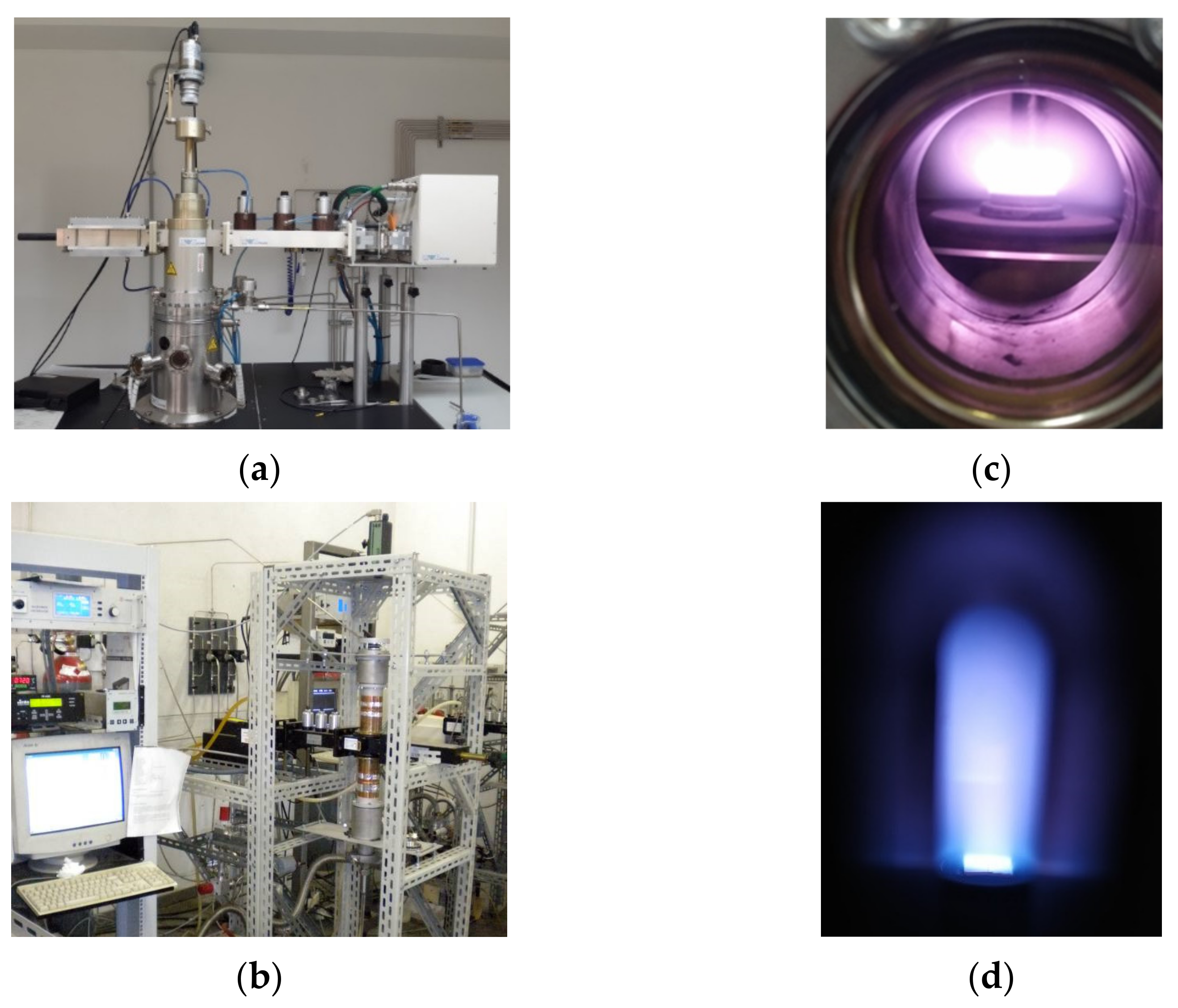
Table 1.
Diamond parameters 1.
| Parameter | Value |
|---|---|
| Atomic Number | 6 |
| Eg at 300 K (eV) | 5.470 |
| Density (g·cm−3) | 3.515 |
| εp (eV) | 13 |
| Fusion temperature (°C) | 4100 |
| Electron mobility (cm2V−1s−1) at 300 K | 1800–2200 |
| Hole mobility (cm2V−1s−1) at 300 K | 1200–1600 |
| Breakdown voltage (Vcm−1) | >107 |
| Thermal conductivity σT (Wcm−1K−1) | 20 |
| Saturation velocity vsat (cm s−1) | 2.7 × 10⁷ |
| Resistivity ρ (ohm cm) | >1013 |
| Intrinsic carrier density at 300 K (cm−3) | <103 |
| Dielectric constant | 5.7 |
| Energy to displace an atom (eV) 1 | 37.5–47.6 |
1 Reference [84].
Table 2.
Work function for some of the most used metals for depositing electrical contacts on diamond films.
Table 2.
Work function for some of the most used metals for depositing electrical contacts on diamond films.
| Element | Work Function 1 (eV) |
|---|---|
| Al | 4.1 |
| Ti | 4.3 |
| Cr | 4.5 |
| Au | 5.1 |
| Pt | 5.7 |
| Cu | 4.65 |
| Ag | 4.29 |
| Ni | 5.25 |
| W | 4.55 |
| Diamond | 4.8–5.8 |
1 Reference [113].
Table 3.
Parameters of the deep level traps in SCD diamond. The reported data are taken from the references listed in Column 6.
Table 3.
Parameters of the deep level traps in SCD diamond. The reported data are taken from the references listed in Column 6.
| Element | Type | Energy (eV) | σc (cm2) | τD | Reference |
|---|---|---|---|---|---|
| B | Impurity | 0.38 | 3.0 × 10⁻¹⁶ | ≈ms | [158] |
| -- | Defect | 0.31 | ≈3.0 × 10⁻¹⁶ | 0.5 ms | [159] |
| -- | Defect | 0.39 | 3.2 × 10⁻¹⁹ | 13 ms | [157] |
| -- | Defect | 1.14 | 9.5 × 10⁻¹⁴ | ≈76 days | [156] |
| - | Defect | 1.23 | 4 × 10⁻¹³ | ≈13 h | [156] |
| N | Impurity | 1.86 | ----- | ≈2 × 10⁹ y | [157] |
Table 4.
n-Carbon reactions for neutron energy up to 20 MeV. Each column reports the total kinetic energy ET (in MeV) of the reaction products as function of the threshold energy (EThr) which is reported in the first column. ET corresponds to the total amount of energy deposited in the diamond bulk. The Q-value of the various reaction is also reported (in italic).
Qvalue (MeV) | 12C(n,α0)9Be −5.701 | 12C(n,3α) −7.275 | 12C(n,n)12C 0 | 12C(n,p)12B −12.587 | 12C(n,d)11B −13.732 | 13C(n,α)10Be −3.835 |
|---|---|---|---|---|---|---|
| EThr | ||||||
| 4.79 | 1.360 | 0.955 | ||||
| 5.72 | 0.019 | 1.625 | 1.885 | |||
| 5.94 | 0.239 | 1.687 | 2.105 | |||
| 6.3 | 0.599 | 1.789 | 2.465 | |||
| 7.33 | 1.629 | 0.055 | 2.082 | 3.495 | ||
| 7.87 | 2.169 | 0.595 | 2.235 | 4.035 | ||
| 8.3 | 2.599 | 1.025 | 2.357 | 4.465 | ||
| 12.82 | 7.119 | 5.545 | 3.641 | 0.233 | 8.985 | |
| 13.79 | 8.089 | 6.515 | 3.917 | 1.203 | 0.058 | 9.955 |
| 15.52 | 9.819 | 8.245 | 4.408 | 2.933 | 1.788 | 11.685 |
| 15.93 | 10.229 | 8.655 | 4.524 | 3.343 | 2.198 | 12.095 |
| 16.30 | 10.599 | 9.025 | 4.630 | 3.713 | 2.568 | 12.465 |
| 17.99 | 12.289 | 10.715 | 5.110 | 5.403 | 4.258 | 14.155 |
| 18.48 | 12.779 | 11.205 | 5.249 | 5.893 | 4.748 | 14.645 |
| 18.96 | 13.259 | 11.685 | 5.385 | 6.373 | 5.228 | 15.125 |
| 20.54 | 14.839 | 13.265 | 5.834 | 7.953 | 6.808 | 16.705 |
Table 5.
Calculated reaction rates for some reactions occurring in carbon (neutron energy > 5 MeV).
| Reaction | % |
|---|---|
| 12C(n,α) | 4 |
| 12C(n,n′) | 5.5 |
| 12C(n,n) | 70 |
| 12C(n,γ) | 0.009 |
Publisher’s Note: MDPI stays neutral with regard to jurisdictional claims in published maps and institutional affiliations. |
© 2021 by the authors. Licensee MDPI, Basel, Switzerland. This article is an open access article distributed under the terms and conditions of the Creative Commons Attribution (CC BY) license (https://creativecommons.org/licenses/by/4.0/).
Share and Cite
MDPI and ACS Style
Angelone, M.; Verona, C. Properties of Diamond-Based Neutron Detectors Operated in Harsh Environments. J. Nucl. Eng. 2021, 2, 422-470. https://doi.org/10.3390/jne2040032
AMA Style
Angelone M, Verona C. Properties of Diamond-Based Neutron Detectors Operated in Harsh Environments. Journal of Nuclear Engineering. 2021; 2(4):422-470. https://doi.org/10.3390/jne2040032
Chicago/Turabian StyleAngelone, Maurizio, and Claudio Verona. 2021. "Properties of Diamond-Based Neutron Detectors Operated in Harsh Environments" Journal of Nuclear Engineering 2, no. 4: 422-470. https://doi.org/10.3390/jne2040032