Article

Effective Method for Multi-Probe Electrical Measurements of Organic Single Crystals: Four-Terminal Natural Adhesion Contact

1
Department of Electrical and Electronic Engineering, Chiba University, 1-33 Yayoi-cho, Inage-ku, Chiba 263-8522, Japan
2
Center for Analytical Instrumentation, Chiba University, 1-33 Yayoi-cho, Inage-ku, Chiba 263-8522, Japan
*
Author to whom correspondence should be addressed.
Solids 2022, 3(2), 311-318; https://doi.org/10.3390/solids3020022
Submission received: 6 April 2022 / Revised: 12 May 2022 / Accepted: 16 May 2022 / Published: 19 May 2022

Abstract

:
A technique to establish electrical contact and perform multi-probe electrical measurements (e.g., four-probe measurements), even at low temperatures, is presented in this work. The natural adhesion contact (NAC) is applicable to the wide range of dimensions of organic crystals. Furthermore, the precise electrode patterns required to carry out multi-probe measurements are guaranteed, in contrast to fine conductive paste painting methods. We demonstrate four-probe electrical measurements of α -(BEDT-TTF) 2 I 3 (where BEDT-TTF = bis(ethylenedithio) tetrathiafulvalene) at temperatures down to 100 K. The obtained temperature dependence showed a steep meta l–insulator transition and exhibited zero hysteresis throughout several measurement sequences.

1. Introduction

Contact resistance is a major issue when conducting electrical measurements because such resistance is sometimes nonnegligible. During the early stages of research in this field, lamination of a thin rubrene single crystal onto an electrode-prepared substrate was demonstrated to be very effective [1,2,3,4]. However, the application of this method was restricted to very thin (less than 1 μ m) organic single crystals because thicker crystals never adhere to the surface of the substrate. Many organic crystals are not necessarily thin flake-like forms. Therefore, this method was not universally applicable. From another perspective, the use of fine drawings of conductive paste on the surfaces of organic crystals was also an effective method to establish Ohmic contacts. The technical levels of these drawings were very high [5,6,7,8,9]. However, this approach had a critical issue in terms of reproducibility. Fine drawing techniques using conductive paste have limiting factors related to handwriting, jig limitations, and paste fluidity. Therefore, a reproducible methodology is required to establish the electrical contacts suitable for a wide range of organic crystals, from thin-flake-like microcrystals to thick or bulk-like crystals. This paper demonstrates that our method is sufficiently well in measuring the temperature dependence of four-probe electrical conductivity measurements of organic charge transfer complexes, covering a wide range of electrical conductivity and temperature variation. This paper emphasizes that this method is stable even at low temperatures, reproducible in 3 thermal cycles, and effective for bulk crystals. Therefore, this contact is also effective in measuring basic electrical properties compared to the research works with laminated devices [10,11,12,13,14].

2. Experimental Details

A photograph of the NAC and its basic configuration are shown in Figure 1a,c, respectively. The NAC is composed of a parylene thin film with a fine multiple-terminal electrode pattern [15,16,17,18,19] (see Figure 1b) fabricated on its surface. The procedure used to fabricate the NAC is explained below. First, we prepared a glass substrate called the ‘preparation substrate’. The preparation substrate was cleaned and immersed in a stripping solution of photoresist that makes the parylene thin film be easily removed from the substrate in the final step. Vapor deposition formed the 900-nm-thick parylene thin film on the preparation substrate. The reasons we used parylene have several points. First, parylene is a hard polymer, so the thin Au electrode pattern does not break when the NAC is peeled off from the preparaton substrate. If the soft polymer was used, Au electrode was broken and exfoliated because of the share strain induced at the Au/parylene interface. Second, the photolithography process can be adequately executed on the parylene surface. Third, parylene thin film is conformally formed from the gas phase on the Au patterned electrodes. And also, parylene thin film is chemically stable and mechanically flexible.Subsequently, an Au thin film (30 nm) was formed on the parylene surface by vacuum deposition, and the Au four-probe electrode pattern (Figure 1b) was formed using standard photolithography and etching processes. Then, as shown in Figure 1a, the parylene thin film was carefully peeled off from the preparation substrate using Kapton adhesive tapes around the periphery as a reinforcement to ensure that the thin parylene film was not destroyed during peeling. After peeling, the NAC was laminated onto the surface of an organic crystal (Figure 1d) using our hand made jig (shown in Figure 2a,b), which is equipped with a four-axis microstage and a digital microscope to align and center the organic crystal and lower the NAC onto the micrometer-sized crystal. As a result, we obtained the sample as illustrated in Figure 1e). The organic crystal was adhered to the surface of a polydimethylsiloxane (PDMS)-coated Neoplim film (Mitsubishi Gas Chemical Company, Inc., Tokyo, Japan ) beforehand. The NAC is aligned and carefully placed in the center of the tiny crystal. Therefore, natural adhesion holds the NAC tightly on the crystal surface. We do not use any adhesion agents in this process. This means that we can even delaminate the NAC from the crystal surface and place it again. However, particles from the atmosphere and crystal fragments tend to stick on the NAC surface during the reuse process. These surface particles inhibit establishing sufficient electrical contact by a natural adhesion. In addition, although we sometimes find that a few air bubbles are confined in the NAC, these confined bubbles can be eliminated through careful vacuum evacuation. After laminating the NAC onto the crystal surface, the sample was placed on the sample stage of a cryostat (Optistat CF-V, Oxford Instruments, Abingdon-on-Thames, UK ). The sample temperature was controlled precisely using a combination of a liquid nitrogen flow and a temperature controller (ITC 503, Oxford Instruments) with a control sequence. Because the variation in the electrical conductivity in the metal–insulator transition temperature region is very steep, we paid close attention to the setting of our temperature control sequence. We established three parameters, comprising the target temperature ( T set ), the wait time ( t wait ), and the temperature tolerance ( Δ T ), to control the sample temperature precisely. After reaching T set , the control sequence waited for 1 min plus t wait . Subsequently, the temperature was measured three times at 15 s intervals. When the deviation of the measured temperature was less than Δ T , the control sequence then executed the four-probe electrical measurements; otherwise, the control sequence waited for t wait and then checked the temperature three times at 15 s intervals again to confirm that the deviation was less than Δ T ; this sequence was repeated until the required condition was satisfied. In this way, the temperature precision of our measurements was in the 0.07–0.09 K range throughout a single series of measurements. Figure 2c shows an optical micrograph of the NAC adhered to the organic charge transfer complex crystal. The charge transfer complex used in this work was the α -(BEDT-TTF) 2 I 3 (where BEDT-TTF = bis(ethylenedithio) tetrathiafulvalene) single crystal, which is well known to exhibit a meta l–insulator phase transition due to the charge ordering [20,21,22,23,24,25,26,27,28]. Single crystals of α -(BEDT-TTF) 2 I 3 were grown by the electrochemical method [20]. We collected several hundred-micrometer crystals from the electrochemical cell.The wide electrodes shown at the left and right edges of the crystal are the electrical current application electrodes, and the two pairs of fine electrodes shown at the top and bottom edges of the crystal are used to detect the electrical potential difference and thus conduct the four-probe electrical resistance measurements. In this optical micrograph, the width of the narrow electrode and the minimum separations are 20 μ m and 60 μ m, respectively. This level of fine drawing is too difficult to reproduce on the crystal surface when using the conductive paste approach.

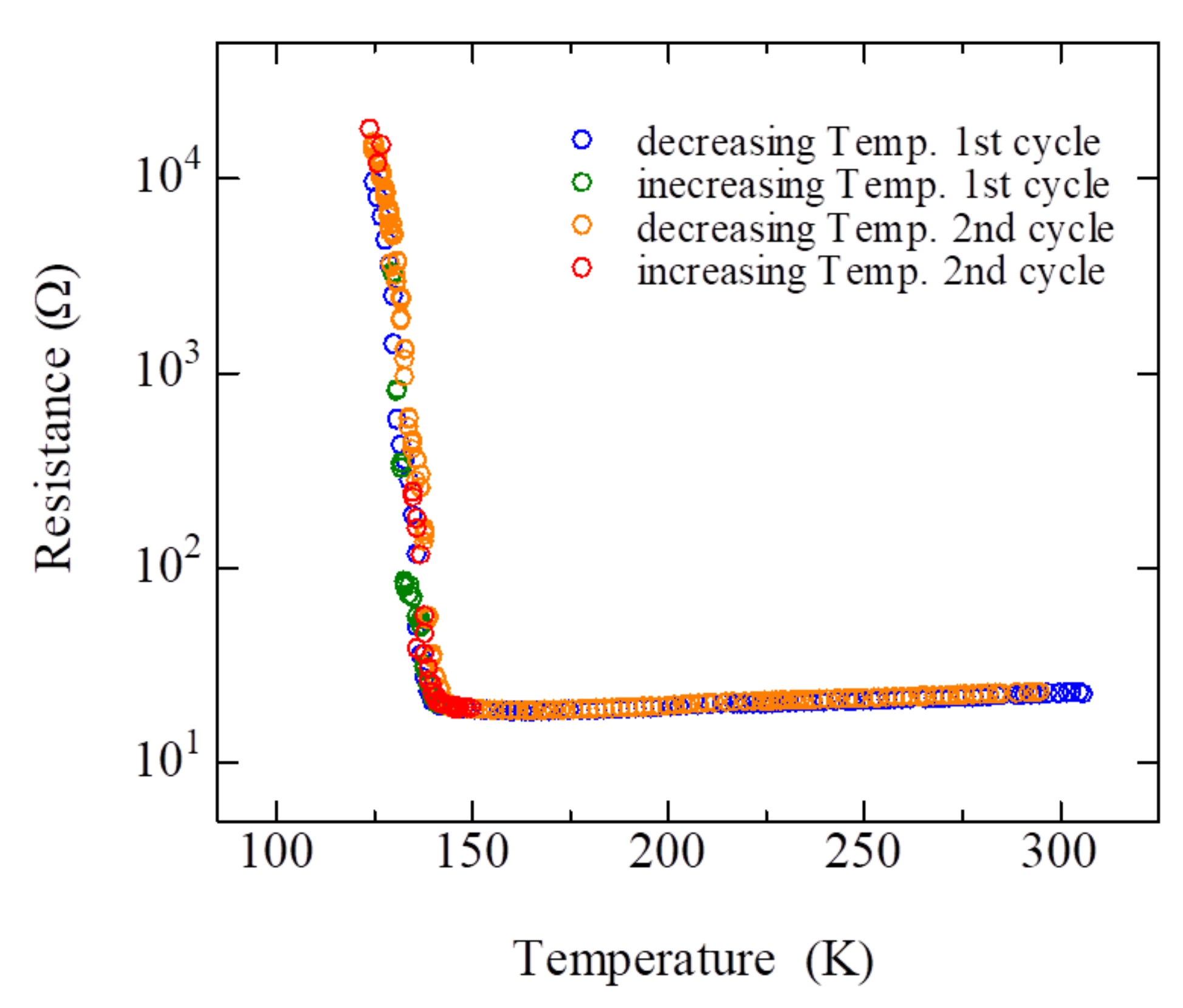
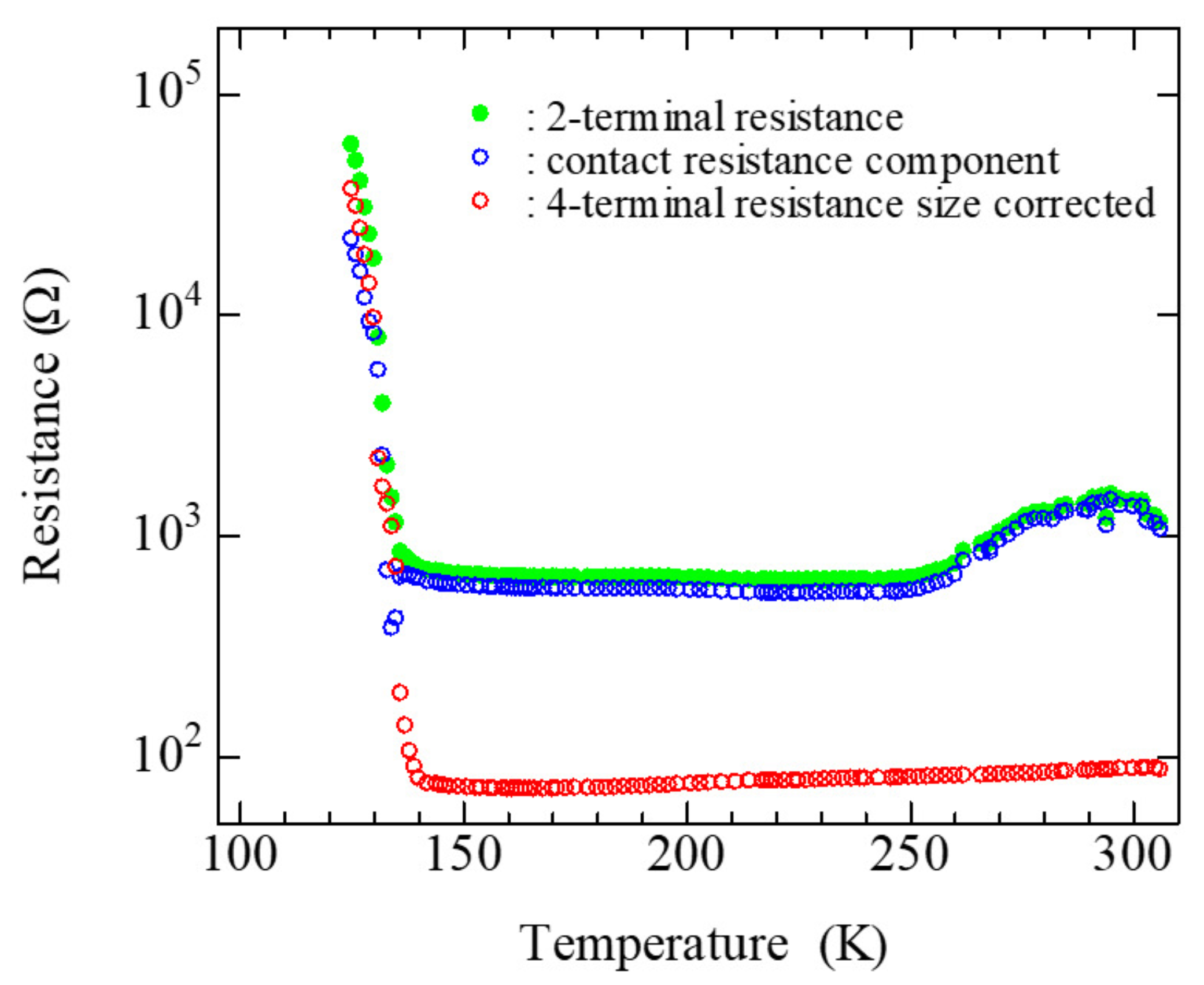
3. Results and Discussion

Figure 3 shows the temperature dependence of the four-probe electrical resistance of the α -(BEDT-TTF) 2 I 3 single crystal measured using the NAC. The meta l–insulator phase transition is observed clearly at approximately 140 K. The metallic temperature dependence of the electrical resistance above 140 K is clearly seen. These temperature dependences have been observed in previous research works [20,29,30]. Therefore, the NAC’s four-probe electrical measurements work sufficiently well, even at low temperatures. Additionally, we have advantages in terms of the size and shape precision of the electrodes, which enabled precise determination of the electrical conductivity and prevented chemical or thermal damage when compared with the conventional methods that apply conductive paste or involve thermal evaporation metals. In fact, before we started this investigation, we were anxious about the availability of the NAC in the low-temperature region because of both the differences in thermal expansion among the NAC, the crystal and the substrate, and the loss of flexibility of the NAC itself. The result showed that these factors of the NAC are negligibly small because of both its small volume and its flexibility due to its thinness. As a result, the availability of the NAC for use in the low-temperature region was successfully demonstrated for a wide range of resistance values from 10 1 up to 10 4 Ω . Additionally, we considered the temperature dependence of the contact resistance. By subtracting the four-probe resistance from the two-terminal resistance with appropriate consideration of the channel length, we extracted the temperature dependence of the contact resistance component. Figure 4 shows the temperature dependences of the two-terminal resistance, the four-terminal resistance component, and the contact resistance component observed in α -(BEDT-TTF) 2 I 3 . As the results clearly show, the contact resistance dominates the two-terminal total resistance above T MI and has little temperature dependence; in contrast, below T MI , the bulk resistance component dominates the observed electrical resistance because of the rapid increase in the bulk resistance, which indicates that the contact resistance is affected by the bulk electronic phase. A comparison of the temperature dependence of the bulk, contact, and total resistances in Figure 4 shows that the bulk resistance clearly exhibits a metallic temperature dependence above T MI . In contrast, the contact resistance does not exhibit such a metallic temperature dependence above T MI . Consequently, the total temperature dependence of electrical resistance above T MI does not show a metallic temperature dependence. This indicates that it is easy to miss an intrinsic temperature dependence if only two-terminal measurements are performed. Therefore, applying four-terminal measurements for a wide range of tiny crystals is expected. This technique is applicable to a wide range of crystals. The NAC well adheres on any surface, from bulky to flake-like crystals, because NAC itself is sufficiently thin and flexible like a cling film. Therefore, NAC is useful for multi-probe electrical measurement for organic crystals with a sufficient mirror surface area. For example, in our trial, electrical measurement of bulky β -(BEDT-TTF) 2 PF 6 crystal around the meta l–insulator transition temperature (about 295 K) was also obtained. In this paper, we showed the result of more severe conditions because NAC has to be both stable and flexible to obtain the electrical properties of α -(BEDT-TTF) 2 I 3 below 140 K. Our NAC offers an alternative to obtaining the precise electrical characteristics of such crystals.

4. Conclusions

We have indicated a technique to establish multiple electrical contacts to a wide range of organic crystals, even for crystals of several hundred micrometers in size. The NAC sticks to an organic crystal surface by natural adhesion. This means neither thermal nor chemical damage occurs when forming an electrical contact with an organic crystal. The NAC can even be delaminated from the crystal without damage. Additionally, we have demonstrated that the NAC is stable and effective even for low-temperature measurements.

Author Contributions

Formal analysis and investigation, H.W., S.U. and M.S.; resources, H.M.; Writing—original draft preparation, M.S. and H.W.; writing—review and editing, M.S. and K.K.; supervision, K.K.; funding acquisition, K.K. and M.S. All authors have read and agreed to the published version of the manuscript.

Funding

This research was financially supported by a Grant-in-aid for Scientific Research (#17H02760) from the Ministry of Education, Culture, Sports, Science & Technology, Japan.

Institutional Review Board Statement

Not applicable.

Informed Consent Statement

Not applicable.

Data Availability Statement

The data presented in this study are available on request from the corresponding author.

Acknowledgments

The authors thank Yuto Tanino, Ryoma Ishii, Daiki Yamamoto, Takahiro Ueda, and Yugo Okada for their experimental help. We thank David MacDonald, from Edanz Group (https://en-author-services.edanzgroup.com/, accessed on 7 November 2021) for editing a draft of this manuscript.

Conflicts of Interest

The authors declare no conflict of interest. The funders had no role in the design of the study; in the collection, analyses, or interpretation of data; in the writing of the manuscript, or in the decision to publish the results.

References

  1. Takeya, J.; Goldmann, C.; Haas, S.; Pernstich, K.P.; Ketterer, B.; Batlogg, B. Field-induced charge transport at the surface of pentacene single crystals: A method to study charge dynamics of two-dimensional electron systems in organic crystals. J. Appl. Phys. 2003, 94, 5800–5804. [Google Scholar] [CrossRef] [Green Version]
  2. Takeya, J.; Nishikawa, T.; Takenobu, T.; Kobayashi, S.; Iwasa, Y.; Mitani, T.; Goldmann, C.; Krellner, C.; Batlog, B. Effects of polarized organosilane self-assembled monolayers on organic single-crystal field-effect transistors. Appl. Phys. Lett. 2004, 85, 5078–5080. [Google Scholar] [CrossRef] [Green Version]
  3. Takeya, J.; Tsukagoshi, K.; Aoyagi, Y.; Takenobu, T.; Iwasa, Y. Hall Effect of Quasi-Hole Gas in Organic Single-Crystal Transistors. Jpn. J. Appl. Phys. 2005, 44, L1393. [Google Scholar] [CrossRef] [Green Version]
  4. Sundar, V.C.; Zaumseil, J.; Podzorov, V.; Menard, E.; Willett, R.L.; Someya, T.; Gershenson, M.E.; Rogers, J.A. Elastomeric Transistor Stamps: Reversible Probing of Charge Transport in Organic Crystals. Science 2004, 303, 1644–1646. [Google Scholar] [CrossRef] [Green Version]
  5. Takafumi, A.; Emiko, O.; Zh, N.B.; Hayao, K.; Takafumi, M.; Madoka, T. Electrical Properties of an Organic Conductor, β’- (BEDT-TTF)2ICl2 up to 10 GPa. Chem. Lett. 2000, 29, 406–407. [Google Scholar]
  6. Suda, M.; Kawasugi, Y.; Minari, T.; Tsukagoshi, K.; Kato, R.; Yamamoto, H.M. Strain-Tunable Superconducting Field-Effect Transistor with an Organic Strongly-Correlated Electron System. Adv. Mater. 2014, 26, 3490–3495. [Google Scholar] [CrossRef]
  7. Suda, M.; Yamamoto, H.M. Field-, strain- and light-induced superconductivity in organic strongly correlated electron systems. Phys. Chem. Chem. Phys. 2018, 20, 1321–1331. [Google Scholar] [CrossRef]
  8. Yoshimoto, S.; Miyahara, R.; Yoshikura, Y.; Tang, J.; Mukai, K.; Yoshinobu, J. Initial gas exposure effects on monolayer pentacene field-effect transistor studied using four gallium indium probes. Org. Electron. 2018, 54, 34–39. [Google Scholar] [CrossRef]
  9. Yoshimoto, S.; Takahashi, K.; Suzuki, M.; Yamada, H.; Miyahara, R.; Mukai, K.; Yoshinobu, J. Highly anisotropic mobility in solution processed TIPS-pentacene film studied by independently driven four GaIn probes. Appl. Phys. Lett. 2017, 111, 073301. [Google Scholar] [CrossRef]
  10. Loo, Y.-L.; Someya, T.; Baldwin, K.W.; Bao, Z.; Ho, P.; Dodabalapur, A.; Katz, H.E.; Rogers, J.A. Soft, conformable electrical contacts for organic semiconductors: High-resolution plastic circuits by lamination. Proc. Natl. Acad. Sci. USA 2002, 99, 10252–10256. [Google Scholar] [CrossRef] [Green Version]
  11. Yamamura, A.; Fujii, H.; Ogasawara, H.; Nordlund, D.; Takahashi, O.; Kishi, Y.; Ishii, H.; Kobayashi, N.; Niitsu, N.; Blulle, B.; et al. Sub-molecular structural relaxation at a physisorbed interface with monolayer organic single-crystal semiconductors. Commun. Phys. 2020, 3, 1–8. [Google Scholar] [CrossRef] [Green Version]
  12. Zaumseil, J.; Someya, T.; Bao, Z.; Loo, Y.-L.; Cirelli, R.; Rogers, J.A. Nanoscale organic transistors that use source/drain electrodes supported by high resolution rubber stamps. Appl. Phys. Lett. 2003, 82, 793–795. [Google Scholar] [CrossRef] [Green Version]
  13. Bernards, D.A.; Biegala, T.; Samuels, Z.A.; Slinker, J.D.; Malliaras, G.G.; Flores-Torres, S.; Abruna, H.D.; Rogers, J.A. Organic light-emitting devices with laminated top contacts. Appl. Phys. Lett. 2004, 84, 3675–3677. [Google Scholar] [CrossRef] [Green Version]
  14. Kim, J.-H.; Sun, Q.; Seo, S. Pressure dependent current-controllable devices based on organic thin film transistors by soft-contact lamination. Org. Electron. 2010, 11, 964–968. [Google Scholar] [CrossRef]
  15. Liu, C.; Chen, C.; Li, X.; Hu, S.; Liu, C.; Huang, K.; Dai, F.; Zhang, B.; Liu, X.; Minari, T.; et al. A General Approach to Probe Dynamic Operation and Carrier Mobility in Field-Effect Transistors with Nonuniform Accumulation. Adv. Funct. Mater. 2019, 29, 1901700. [Google Scholar] [CrossRef]
  16. Li, D.; Li, S.; Lu, W.; Feng, S.; Wei, P.; Hu, Y.; Wang, X.; Lu, G. Rapidly Measuring Charge Carrier Mobility of Organic Semiconductor Films Upon a Point-Contact Four-Probes Method. IEEE J. Electron. Devices Soc. 2019, 7, 303–308. [Google Scholar] [CrossRef]
  17. Hamai, T.; Arai, S.; Hasegawa, T. Effects of tunneling-based access resistance in layered single-crystalline organic transistors. J. Mater. Res. 2018, 33, 2350–2363. [Google Scholar] [CrossRef]
  18. Hamai, T.; Arai, S.; Minemawari, H.; Inoue, S.; Kumai, R.; Hasegawa, T. Tunneling and Origin of Large Access Resistance in Layered-Crystal Organic Transistors. Phys. Rev. Appl. 2017, 8, 054011. [Google Scholar] [CrossRef] [Green Version]
  19. Cho, J.-M.; Mori, T. Low-Temperature Band Transport and Impact of Contact Resistance in Organic Field-Effect Transistors Based on Single-Crystal Films of Ph-BTBT-C10. Phys. Rev. Appl. 2016, 5, 064017. [Google Scholar] [CrossRef]
  20. Bender, K.; Dietz, K.; Endres, H.; Helberg, H.W.; Hennig, I.; Keller, H.J.; Schafer, H.W.; Schweitzer, D. (BEDT-TTF)2+J3-: A Two-Dimensional Organic Metal. Mol. Cryst. Liqid Cryst. 1984, 107, 45–53. [Google Scholar] [CrossRef] [Green Version]
  21. Bender, K.; Hennig, I.; Schweitzer, D.; Dietz, K.; Endres, H.; Keller, H.J. Synthesis, Structure and Physical Properties of a Two-Dimensional Organic Metal, Di[bis(ethylenedithiolo)tetrathiofulvalene] triiodide, (BEDT-TTF)2+ I3-. Mol. Cryst. Liqid Cryst. 1984, 108, 359–371. [Google Scholar] [CrossRef] [Green Version]
  22. Kawakami, Y.; Fukatsu, T.; Sakurai, Y.; Unno, H.; Itoh, H.; Iwai, S.; Sasaki, T.; Yamamoto, K.; Yakushi, K.; Yonemitsu, K. Early-Stage Dynamics of Light-Matter Interaction Leading to the Insulator-to-Metal Transition in a Charge Ordered Organic Crystal. Phys. Rev. Lett. 2010, 105, 246402. [Google Scholar] [CrossRef] [PubMed]
  23. Seo, H. Broken symmetry states in quasi-one-dimensional molecular conductors - competitions, co-existences, and frustration. Physica B 2010, 405, S126–S130. [Google Scholar] [CrossRef]
  24. Wojciechowski, R.; Yamamoto, K.; Yakushi, K.; Inokuchi, M.; Kawamoto, A. High-pressure Raman study of the charge ordering in α-(BEDT-TTF)2I3. Phys. Rev. B 2003, 67, 224105. [Google Scholar] [CrossRef]
  25. Yue, Y.; Yamamoto, K.; Uruichi, M.; Nakano, C.; Yakushi, K.; Yamada, S.; Hiejima, T.; Kawamoto, A. Nonuniform site-charge distribution and fluctuations of charge order in the metallic state of α-(BEDT-TTF)2I3. Phys. Rev. B 2010, 82, 075134. [Google Scholar] [CrossRef] [Green Version]
  26. Ivek, T.; Korin-Hamzic, B.; Milat, O.; Tomic, S.; Clauss, C.; Drichko, N.; Schweitzer, D.; Dressel, M. Electrodynamic response of the charge ordering phase: Dielectric and optical studies of α-(BEDT-TTF)2I3. Phys. Rev. B 2011, 83, 165128. [Google Scholar] [CrossRef] [Green Version]
  27. Tajima, N.; Sugawara, S.; Tamura, M.; Nishio, Y.; Kajita, K. Electronic Phases in an Organic Conductor α-(BEDT-TTF)2I3: Ultra Narrow Gap Semiconductor, Superconductor, Metal, and Charge-Ordered Insulator. J. Phys. Soc. Jpn. 2006, 75, 051010. [Google Scholar] [CrossRef] [Green Version]
  28. Kodama, K.; Kimata, M.; Takahide, Y.; Kurita, N.; Harada, A.; Satsukawa, H.; Terashima, T.; Uji, S.; Yamamoto, K.; Yakushi, K. Charge Transport in Charge-Ordered States of Two-Dimensional Organic Conductors, α-(BEDT-TTF)2I3 and α’-(BEDT-TTF)2IBr2. J. Phys. Soc. Jpn. 2012, 81, 044703. [Google Scholar] [CrossRef]
  29. Ivek, T.; Culo, M.; Kuvezdic, M.; Tutis, E.; Basletic, M.; Mihaljevic, B.; Tafra, E.; Tomic, S.; Lohle, A.; Dressel, M.; et al. Semimetallic and charge-ordered α-(BEDT-TTF)2I3: On the role of disorder in dc transport and dielectric properties. Phys. Rev. B 2017, 96, 075141. [Google Scholar] [CrossRef] [Green Version]
  30. Ishikawa, K.; Hirata, M.; Liu, D.; Miyagawa, K.; Tamura, M.; Kanoda, K. Spin excitations in the quasi-two-dimensional charge-ordered insulator α-(BEDT-TTF)2I3 probed via 13C NMR. Phys. Rev. B 2016, 94, 085154. [Google Scholar] [CrossRef] [Green Version]
Figure 1. (a) Photograph of NAC during the process of being peeled off the preparation substrate. (b) Magnified view of the center of the NAC pattern. D and S denote the drain and source electrodes used as the current application electrodes in four-probe measurements. V 1 –V 4 denote the electrodes for measurement of the electrical potential. Illustrations of (c) the NAC structure and (d) the sample. The NAC is prepared on the glass substrate, peeled off, and then laminated onto the organic crystal using natural adhesion. (e) Cross-sectional view of the sample.
Solids 03 00022 g001
Figure 2. (a) Hand-made jig used to laminate the NAC precisely onto the tiny crystal. The crystal on the substrate is placed on the top plate of the X-Y and θ -stage on the left side, and the NAC is settled on the top fork arm of the Z-stage on the right side. (b) the same jig being viewed from the θ -stage side. The NAC is mounted between the folk arms as it descends onto the crystal via the action of the Z-stage. (c) Optical micrograph of the NAC after adhesion to the organic charge transfer complex. The crystal is shown at the center, and six patterned electrodes are contacting the crystal.
Solids 03 00022 g002
Figure 3. Temperature dependence of four-terminal electrical resistance of α -(BEDT-TTF) 2 I 3 . Both a metallic temperature dependence of the resistance above 140 K and an insulator-like temperature dependence below 140 K are observed clearly. Therefore, the NAC remains stable even at low temperatures. Furthermore, the degradation during the two measurement cycles displayed here is almost negligible, as the results show.
Solids 03 00022 g003
Figure 4. Temperature dependences of the two-terminal resistance, the four-terminal resistance after the channel length correction, and the contact resistance observed in α -(BEDT-TTF) 2 I 3 with the NAC. The contact resistance was extracted by subtracting the four-terminal resistance from the two-terminal resistance.
Solids 03 00022 g004
Publisher’s Note: MDPI stays neutral with regard to jurisdictional claims in published maps and institutional affiliations.

