
Developments in Mask-Free Singularly Addressable Nano-LED Lithography

1
Ernst-Ruska-Centre (ER-C-2), Forschungszentrum Jülich, 52425 Jülich, Germany
2
Jülich-Aachen Research Alliance (JARA), Fundamentals of Future Information Technology, 52425 Jülich, Germany
3
Robert Bosch GmbH, 72760 Reutlingen, Germany
4
Central Facility for Electron Microscopy (GFE), RWTH Aachen University, 52074 Aachen, Germany
*
Authors to whom correspondence should be addressed.
Nanomanufacturing 2024, 4(2), 99-110; https://doi.org/10.3390/nanomanufacturing4020007
Submission received: 27 October 2023
/
Revised: 8 February 2024
/
Accepted: 22 March 2024
/
Published: 22 April 2024
(This article belongs to the Special Issue Feature Papers for Nanomanufacturing in 2023)
Abstract
:LED devices are increasingly gaining importance in lithography approaches due to the fact that they can be used flexibly for mask-less patterning. In this study, we briefly report on developments in mask-free lithography approaches based on nano-LED devices and summarize our current achievements in the different building blocks needed for its application. Individually addressable nano-LED structures can form the basis for an unprecedented fast and flexible patterning, on demand, in photo-chemically sensitive films. We introduce a driving scheme for nano-LEDs in arrays serving for a singularly addressable approach. Furthermore, we discuss the challenges facing nano-LED fabrication and possibilities to improve their performance. Additionally, we introduce LED structures based on a hybrid nanocrystal/nano-LED approach. Lastly, we provide an outlook how this approach could further develop for next generation lithography systems. This technique has a huge potential to revolutionize the field and to contribute significantly to energy and resources saving device nanomanufacturing.
1. Introduction
Although a large amount of work was carried out on the development of optical lithographical techniques during the last half century, there still is a lack of fast and cheap as well as energy and resources saving solutions. Therefore, next developments in this field will be focused on mask-free approaches, which can serve with an unprecedented flexibility in structure patterning on demand. Nevertheless, several “building blocks” are needed for a new generation mask-less approach, before this could be realized. First, the development of group III nitrides material and appropriate epitaxial techniques were successfully driven forward since the end of the 1980’s [1,2,3,4,5,6,7]. Additionally, advanced fabrication technologies are required in the micro- down to the nanoscale device processing. Indeed, sophisticated methods for the fabrication of efficient light emitter sources as well as several approaches to produce them down to the micro- [8,9,10,11,12] and to the nanoscale [13,14,15,16,17,18,19,20] were already achieved. With respect to singularly addressable light emitter sources, Orenstein and co-workers reached an important milestone in their pioneering work where matrix driven arrays with surface emitting laser diodes were developed [21,22,23,24] albeit for signal processing and optical communication. The further developments, which represent a significant step forward, were reported on the arrangement of LEDs in arrays [25,26,27,28,29,30,31] and the possibility to drive them preferably singularly (among others for displays) [32,33,34,35,36,37,38,39,40,41,42,43]. Hence, if all of these “ingredients/building blocks” are available within a lithography system, in principle, next generation lithography can be carried out mask-free, allowing time and resources savings, flexible structure patterning on demand. Indeed J. N. Kurtin presented in 2005 an array of LED structures suitable for such individually addressable lithographical patterning [44]. The application of UV (microscale) LEDs to lithography was also reported [45,46,47,48,49,50,51,52]. Alternative approaches were pursued such as amongst others plasmonic lithography [53]. In 2012 and 2015 we presented a first proof of principle [54,55], where nano-LED devices with diameters ~100 nm arranged hexagonally in arrays were used in the lithographical exposure process for “hole” shaped structure fabrication. A “hole” structure size down to about 400 nm was achieved when the nano-LED sources emitted light with a central wavelength of ~405 nm. Finally, in 2020, we presented for the first time (to the best of our knowledge) nano-LED devices with metallic apertures for the lithographical process in the so-called “near-field” regime [56]. Photochemical reactions initialized by those nano-emitter devices resulted in a space-lateral distribution of photo-induced reactions in the exposed regions of ~75 nm in diameter. This confirms that nano-LED devices with appropriate apertures for near-field applications can be potentially applied in mass-production successfully for nanomanufacturing. Nevertheless, the ultimate demonstration of single photon lithography was up to now/date not demonstrated. Since favorable photochemical reactions could be theoretically driven by single photons, with an appropriate energy in processes where—depending on the molecule cross-section—one or a couple of photons can alter one chemical bond, this technique would allow to enable the era of mass nanomanufacturing for, e.g., molecular electronics. However, in nowadays/conventional photoresists, a higher yield of incident photons is required for the photochemical reaction. Additionally, before this concept can be realized, suitable single photon sources operated at room temperature, and their industrial mass production, have to be developed. Besides other “light emitting” solutions, our previous studies reveal that III-nitride based nano-LEDs are very promising as multifunctional photon emitting devices, which can be used as hybrid photon emitting sources. In such hybrid device architectures, we presented single nano-LED structures driven electrically, and integrated with freestanding CdSe nanocrystals [57]. Such hybrid architectures can serve as testing platforms for the investigation of plasmonic effects. This could be of benefit especially for the sake of field enhancement at the position of a light emitting nanoparticle. Further methods discussed for micro-LEDs with respect to localized surface plasmon enhancement for device improvement [58] and the improvement of light extraction and shaping using metamaterials could in the far future also be applied to nano-LEDs [59] and their employment for future mask-free singularly addressable lithography. Here, in this study, we deliver a short overview/roadmap of the most promising developments in this new arising nanomanufacturing field and present current achievements for (hybrid) nano-LED assisted mask-less lithography.
2. Materials and Methods
The singularly addressable nano-LEDs employed for the mask-free lithography approach were all based on the same parent structure. To this end 2″ c-plane sapphire substrates were chosen and group III-nitride heterostructures were deposited by metalorganic vapor phase epitaxy (MOVPE). First, n-doped GaN 5 × 1018 cm−3 was grown followed by a five-fold superlattice structure consisting of 16 nm GaN barriers and 2.5 nm In0.16Ga0.84N wells. At last, a 250 nm thick GaN layer p-doped to 5 × 1017 cm−3 followed by 20 nm of p+-doped GaN (6 × 1018 cm−3) were deposited.
In the next building block nano-LED devices positioned in arrays were defined by using e-beam lithography to pattern holes in the PMMA 600 K resist and subsequent developing in AR 600-55 developer. After the physical vapor deposition (PVD) of Ni and the lift-off process, 100 nm Ni caps were formed serving as the etching mask for the space definition/formation of nano-LEDs. In a first step, reactive ion etching was performed up to the bottom n-doped GaN contact layer in an Oxford Plasmalab 100 reactor with an inductively coupled plasma (ICP) 180 source at a pressure of 4 µbar, a sample temperature of 5 °C, a chlorine:argon gas mixture of 16:4, and an ICP power of 750 W [18,60]. In the next step, n-doped GaN bottom contacts (word lines) were defined with the help of optical lithography. The photoresist AZ 5206 was chosen followed by developing in a standard developer (MIF 326). An Ar-ion beam etching process (Ar-IBE, Oxford Instruments, 200 V, 20 mA) was carried out down to the sapphire substrate. The nano-LEDs were insulated from neighbors using hydrogen silsesquioxane (HSQ), which was spun onto the structured template to obtain a planar surface. The template was then annealed to induce the chemical reaction to the SiO2 layer. At last, transparent top contacts (bit lines) were prepared using optical lithography and the same photoresist and developer mentioned above followed by deposition of the transparent Ni/Au (5 nm/5 nm) top-contact metallization and a subsequent conventional rapid thermal annealing process. The nano-LEDs were annealed locally with the laser micro-annealing (LMA) process presented earlier [60]. Furthermore, it becomes possible to fabricate an array of hybrid nano-LEDs. A micropipette is used [57,61] to apply the polymer—nanocrystal suspension, the details and procedure of which will be published separately.
The structures were inspected with optical microscopy and scanning electron microscopy (SEM). Furthermore, micro-photoluminescence (µ-PL) and micro-electroluminescence spectroscopy (µ-EL) were carried out at room temperature to assess the fabrication procedure and to evaluate the long-term stability of the nano-LED performance. For both the LMA process as well as the µ-PL and µ-EL spectroscopy experiments, a confocal Raman and photoluminescence spectrometer (Renishaw inVia FSM REFLEX, New Mills, Gloucestershire, UK) was used which was equipped with a HeCd laser (325 nm) and a CCD detector [60].
The basic idea behind mask-free singularly addressable LED lithography is presented in Figure 1. In general, nano-LEDs are arranged in a crossbar geometry, allowing for their individual driving after the fabrication of “word” and “bit” lines. In such a way, different patterns can be “created” on demand flexibly. This lithographical approach has the potential to simplify and accelerate patterning significantly compared to conventional mask-based lithographical processes, since large areas of the photosensitive films/photoresists can be exposed at the same time.
3. Results
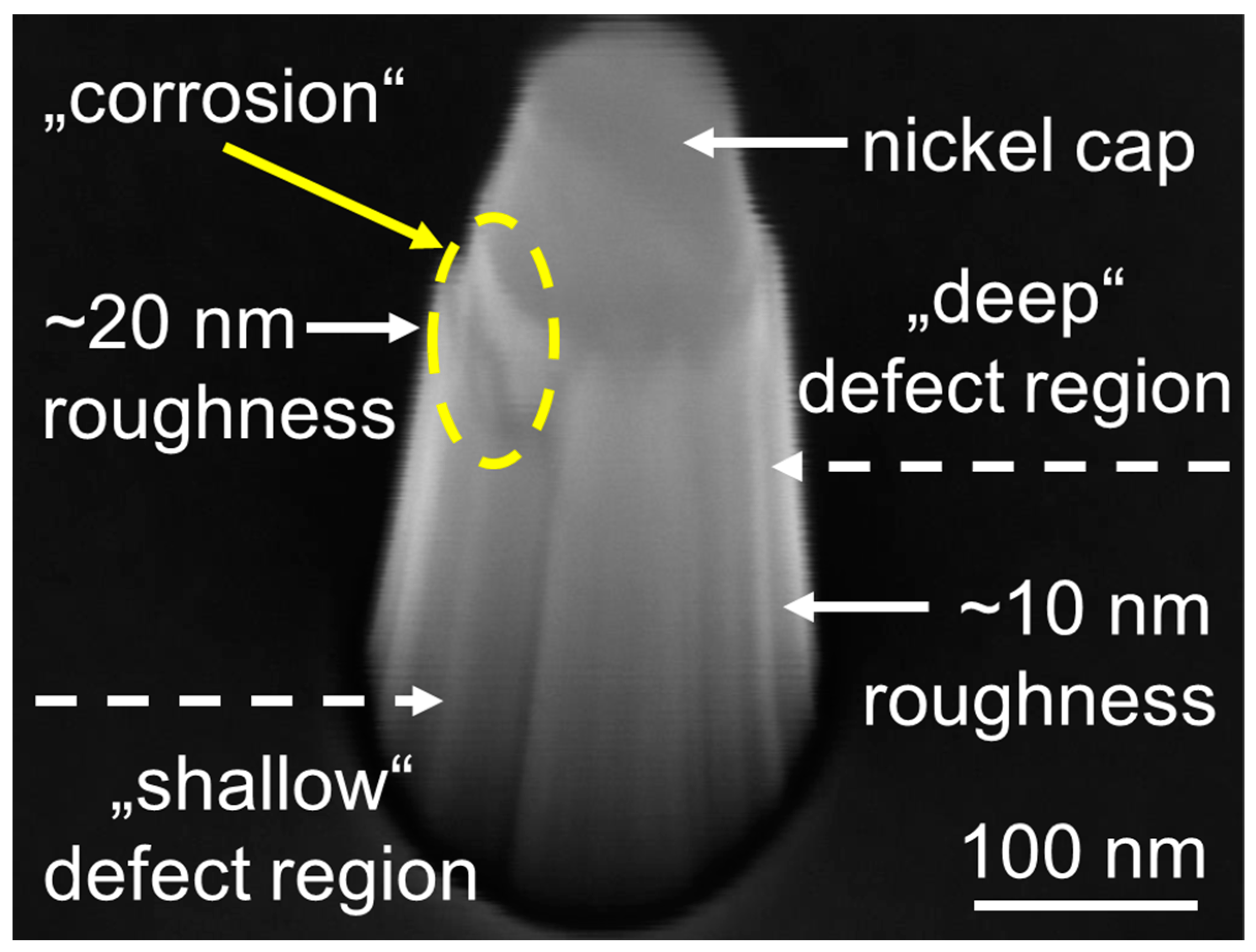
It is well known that conventional argon ion beam etching (IBE) as well as reactive ion etching (RIE) used for the spatial definition/formation of nano-LEDs leads to a degradation of the devices’ optical properties which is manifested by a significant decrease in their electroluminescence [57,60,62]. Here, in this study, SEM investigations (Figure 2) reveal inhomogeneous surface nano-LED morphology. This inhomogeneity is a result of the surface damage of the combined physical and chemical reactive ion etching processes. These physical and/or most probably chemical processes take place along the whole surface of the nano-LED. However, a physical damage up to 20 nm was observed only at the “top” of the nanostructure regions. This can be explained by the longer times that the tops of the nanostructures are exposed to the etching reactants during the RIE processes. Deeper regions close to the nano-LED’s “base” are affected only by “shorter” etching times (i.e., a shorter exposure) which is manifested among others by “smoother” surface morphology. With respect to the morphology of the nano-LEDs it must be taken into account that the LED parent structure used as the basis for the etched nano-LEDs has a high defect density and defects themselves will most probably affect their morphology. Here it should be noted, that even though the SEM inspection over a large area reveals almost individual surface morphology (damage) for every nano-LED structure, nevertheless, the nano-LEDs all have the same average dimensions (e.g., top and bottom diameter, total height). Therefore, the SEM image in Figure 2 is only an example of such a nano-LED. A comprehensive analysis on the causes of the defects is in preparation and will be the subject of a future report. The photoluminescence measurements presented e.g in our earlier stuides [60,62] reveal the negative effect of RIE processes on the optical and electrical device characteristics. Hence, alternative technological steps are required to “heal” such “defect” structures. Previously, we presented such an approach—a local laser micro annealing (LMA) procedure [60], a next building block, which will be described in the following section. After the nano-LED’s device definition/formation, n-GaN regions located at a depth of ~1 µm schematically shown in Figure 1, are defined by conventional photolithography and a subsequent Ar-IBE procedure. An example for nano-LED structures located on the “word line” is presented in Figure 3. Details of the structures presented in Figure 3B reveal that the etched regions do not reach the nano-LED structures themselves. The Ar-IBE etching process leads to a significant surface damage only in the n-GaN/sapphire interface region (Figure 3C) as well as in “deeper” regions where the n-GaN layer was already fully removed and the sapphire substrate was reached. Here it should be noted, as is evident in Figure 3B, the defined n-GaN layer regions, which later serve as a “word line”, are not affected by the etching technology. An example for the large array of “buried” nano-LED structures with a diameter of ~100 nm is presented in Figure 4. All devices are encompassed in a SiO2 layer as can be seen in detail in Figure 5. It serves on the one hand for electrical insulation and on the other hand as a planarization layer for the subsequent final top contact and bit line processing. These “buried” nano-LEDs arranged in large testing arrays were subsequently characterized by micro-photoluminescence (micro-PL) spectroscopy at room temperature. An example for a micro-PL mapping is presented in Figure 6. Details are discussed in the following section “Discussion”. Furthermore, after top contact metallization, apertures are formed, which can take up the polymer—nanocrystal suspension. Figure 7a presents a “buried” single nano-LED structure with an aperture filled with polymer—nanocrystal suspension in detail and Figure 7b shows exemplarily a layout for hybrid nano-LEDs singularly addressable by the respective “word” (grey) and “bit” lines (gold). This device layout represents a first example for “combined” hybrid nano-LED structures. We demonstrated the nano-LEDs with a metallic aperture in our previous report [56]. The fabrication process and characterization of hybrid nano-LED devices was reported in [57]. The combination of both device architectures results in the structure presented in detail in Figure 7a. If the appropriate nanocrystals with different materials and/or diameters are locally injected in the targeted nano-LED´s aperture regions, such combined structures allow to create “multicolor” light emitter arrays suitable for a lithographical process where “mixtures” of photosensitive films or layer-stacks could be selectively photo-chemically altered. This would allow the processing of complex patterning architectures simultaneously in the future.
4. Discussion
Developments in mask-free singularly addressable nano-LED lithography with respect to its future implementation are closely connected to a number of challenges such as the reproducibility and control of the fabrication process, its simplicity and efficiency as well as the long-term stability of the light emitter sources. Therefore, selected/critical steps involved are discussed and assessed in the following. As we already mentioned in the previous section, conventional reactive ion etching (RIE) is used for the spatial definition and/or structure formation of nano-LED devices. The optimization of the nanomanufacturing/etching procedure is key to obtaining nano-LEDs, that can be (singularly) adressable [18,55]. The nano-LED/structure definition is carried out up to the n-doped GaN contact layer which should not degrade by the etching process. For the preparation of the nano-LEDs into individual “word lines”, etching in a further step must be carried out (Ar-IBE procedure) to define the respective contact layer.
Therefore the sapphire substrate has to be reached to ensure the insulation of the lines. The principle of this device architecture is presented in Figure 1. It needs to be taken into account that a redeposition of etched GaN takes place along the lines (Figure 3C in detail). In spite of careful etching optimization, the etching procedure nevertheless leads to a significant decrease in the nano-LEDs’ electroluminescence intensity. Hence, alternative fast and efficient technological procedures need to be applied for device performance improvement. A number of technological approaches are available to heighton the efficiency of micrometer and nano-sized LED structures. One of these is the precise local laser micro annealing (LMA) procedure, a building block the full potential of which has still to be uncovered. As we already mentioned in Section 3 (Results) the etching process for the formation and fabrication of nano-LED devices leads to a degradation of their optical properties [60]. Since various emerging applications such as “nano-LED singularly addressable lithography” introduced in this work and others require full control and/or tuning of the electroluminescence intensity of individual devices, a suitable technology needs to be developed. The application of the LMA process resulted in meeting the requirement and the expected optical properties can then be achieved. In our previous study [60], the simple model based on a defect layer depth described the direct correlation between the suppression of radiative recombination as a follow of the MQW’s effective volume reduction after the etching procedure. As a result, the respective effective volume can be increased after the LMA procedure was applied locally for the individual nano-LED structures. This effect was confirmed by our photoluminescence studies and an about 70% decrease in the defect layer depth was evaluated [60]. Hence, the application of the LMA is advantageous also in the fabrication of the singularly addressable nano-LED architecture, since the precise control of the EL intensity of all the individual devices reduces along the way the overall device power consumption as well as increases their lifetime as it was reported previously [60]. Nevertheless, LMA is not limited only to nano-LED devices, this technique can be applied also to transmistor based devices forming core components for optical computing [63,64]. The conditioning of LED devices plays [60] an important role also in the development of novel correlative characterization techniques as we already presented in our previous studies [60,62]. Unfortunately, the formation of nano-LED devices remains a crucial point in spite of all of these development efforts. This is demonstrated in Figure 2.
After SEM inspection of the fabricated nano-LEDs it was confirmed that the RIE procedure has to be further optimized in future—targeting the aim to prevent surface and/or detrimental damage especially in the MQW region. In this “building” block, special attention has to be paid also to alternative gas mixtures for RIE, which could be used instead of the conventional one. As a consequence of the etching procedure and the damage related to the chemical and physical etching processes, the distribution of the photoluminescence differs strongly over the array as can be seen in Figure 6a. It presents an intensity mapping of the single nano-LEDs in the array at the individually measured points. The mapping consists of hundreds of PL-spectra, which were then evaluated for the map presentation. Where only GaN remains after etching, a high GaN band edge luminescence (denoted in blue) is observed. Defect luminescence (emission maxima in the PL spectra range of ~540–600 nm, denoted in green-red) is detected presumably at the circumference of the nano-LEDs and PL emission maxima (~440–445 nm) denoted in pink/violet color are attributed to the MQW luminescence of the nano-LEDs. The mapping discloses that radiative recombination is suppressed due to the damage induced by the etching process as was previously reported [60]. Therefore, a further building block—the LMA technique—has to be applied in the nano-LED’s device processing as well. A simple model showing the effect of the reduction of defect layer depth after laser micro annealing was introduced in our previous work [60]. The subsequent micro photoluminescence studies disclosing an increased photoluminescence intensity indicated that the LMA process has a direct impact on the curing of etching related defects. These are deemed responsible for the suppression of radiative recombination in the nano-LED devices. Photoluminescence measurements on the nano-LED structures revealed [60] that by using the LMA procedure, the nano-LED properties were enhanced in comparison to their non-locally annealed counterparts. According to the simple model mentioned above, the integrated PL-intensity enhancement of the nano-LEDs observed can be explained by the reduction of the defect layer depth from ~17 nm to ~5 nm [60]. Furthermore, the application of the LMA process to the nano-LEDs leads to a current increase up to ~3.7-fold at 5 V [60]. Additionally, only a “moderate reduction” ~15% in electroluminescence intensity (during continuous wave long term operation for 5000 h) in comparison to its non-locally annealed counterpart (~50%), was demonstrated. Furthermore, micro-Raman thermography investigations performed on single nano-LED structures (after the LMA procedure) revealed an up to 60 K decrease in work temperature [60]. This is advantageous, since lithographical processes, in general, are temperature “sensitive”. One other important issue are the long-term “costs” for such lithographical techniques. They can be decreased significantly if the device lifetime, stability as well as reliability could be increased in comparison to/with existing “light/exposure” sources used for conventional lithography. Indeed, it has already been disclosed that the application of the LMA procedure for nano-LED devices could be of a large benefit. During up to 5000 h of operation, the electroluminescence of such nano-LEDs barely decreases (i.e., the optical properties do not degrade). This means that the nano-LED lifetime and reliability increase by local annealing with the LMA process. The performance of such locally annealed nano-LEDs renders them suitable for a future employment as a key component for on chip integrated electro-optic convertors [62]. Additionally, they may achieve still unprecedented importance in the development of novel optical computing architectures based on transmistor/all optical switch units.
5. Conclusions
In this contribution, we discussed the technology of nano light emitting diodes (nano-LEDs) for future mask-free singularly addressable lithographical techniques. Our previous studies revealed that the nano-LEDs are suitable devices for the local initialization of photochemical reactions. Hence, advanced “LED-based” lithographical techniques such as for applications in the “near” field regime could potentially revolutionize the fabrication of nanodevices. Ultimately, if appropriate arrays of single photon sources could be developed and integrated into a singularly addressable approach, they could serve for future molecular lithographical/patterning techniques. In addition, inspired by the technology developed for color displays, “light” sources of different wavelengths can be applied principally in the future to “multi-color” singularly addressable nano-LED lithographical techniques. Nevertheless, the development of the LEDs’ device nanomanufacturing technologies are not limited only to the in this study presented advanced lithographical techniques. They are also driven/motivated by strong technological needs and demand on highly efficient, energy and resources saving solutions as well. Highly resolved illumination microscopy and a large range of spectroscopic and diagnostic methods such as in security (e.g., gas and drugs monitoring) and/or where localized light sources attaining deeper insights into biological cells are needed, are just a selection of applications in which the nano-LEDs could gain importance. They could potentially represent key/basic components in sophisticated technological architectures necessary for future developments towards on chip optical communication, advanced data processing and storage for optical and/or neuromorphic computing as well. Finally, singularly addressable nano-LEDs introduced in a driving scheme for the lithographical approach in this work could also be of benefit in emerging optogenetic and neuronal stimulation applications. The key to their successful application will be, however, the development of such nanofabrication technologies as presented in this report.
Author Contributions
Conceptualization, M.M. and H.H.H.; methodology, M.M. and H.H.H.; validation, M.M.; investigation, M.M., H.H.H. and A.W.; resources, J.M.; data curation, M.M. and H.H.H.; writing—original draft, M.M. and H.H.H.; writing—review and editing, M.M., H.H.H. and J.M.; supervision, H.H.H. and J.M. All authors have read and agreed to the published version of the manuscript.
Funding
This research received no external funding.
Data Availability Statement
Experimental data are available upon reasonable request from the corresponding authors.
Conflicts of Interest
Author Andreas Winden was employed by the Robert Bosch GmbH. The remaining authors declare that the research was conducted in the absence of commercial or financial relationships that could be construed as a potential conflict of interest.
References
- Amano, H.; Akasaki, I.; Hiramatsu, K.; Koide, N.; Sawaki, N. Effects of the buffer layer in metalorganic vapour phase epitaxy of GaN on sapphire substrate. Thin Solid Films 1988, 163, 415–420. [Google Scholar] [CrossRef]
- Amano, H.; Kitoh, M.; Hiramatsu, K.; Akasaki, I. Growth and Luminescence Properties of Mg-Doped GaN Prepared by MOVPE. J. Electrochem. Soc. 1990, 137, 1639–1641. [Google Scholar] [CrossRef]
- Nakamura, S.; Mukai, T.M.T.; Senoh, M.S.M. High-Power GaN P-N Junction Blue-Light-Emitting Diodes. Jpn. J. Appl. Phys. 1991, 30, L1998–L2001. [Google Scholar] [CrossRef]
- Akasaki, I.A.I.; Amano, H.A.H. Crystal Growth and Conductivity Control of Group III Nitride Semiconductors and Their Application to Short Wavelength Light Emitters. Jpn. J. Appl. Phys. 1997, 36, 5393–5408. [Google Scholar] [CrossRef]
- Kukushkin, S.A.; Osipov, A.V.; Zhukov, S.G.; Zavarin, E.E.; Lundin, W.V.; Sinitsyn, M.A.; Rozhavskaya, M.M.; Tsatsulnikov, A.F.; Troshkov, S.I.; Feoktistov, N.A. Group-III-nitride-based light-emitting diode on silicon substrate with epitaxial nanolayer of silicon carbide. Tech. Phys. Lett. 2012, 38, 297–299. [Google Scholar] [CrossRef]
- Wang, Q.; Yuan, G.-D.; Liu, W.-Q.; Zhao, S.; Zhang, L.; Liu, Z.-Q.; Wang, J.-X.; Li, J.-M. Monolithic semi-polar (1101) InGaN/GaN near white light-emitting diodes on micro-striped Si (100) substrate. Chin. Phys. B 2019, 28, 087802. [Google Scholar] [CrossRef]
- Hu, N.; Dinh, D.V.; Pristovsek, M.; Honda, Y.; Amano, H. How to obtain metal-polar untwinned high-quality (10 −13) GaN on m-plane sapphire. J. Cryst. Growth 2019, 507, 205–208. [Google Scholar] [CrossRef]
- Wang, Y.; Zhu, G.; Cai, W.; Gao, X.; Yang, Y.; Yuan, J.; Shi, Z.; Zhu, H. On-chip photonic system using suspended p-n junction InGaN/GaN multiple quantum wells device and multiple waveguides. Appl. Phys. Lett. 2016, 108, 162102. [Google Scholar] [CrossRef]
- Olivier, F.; Tirano, S.; Dupré, L.; Aventurier, B.; Largeron, C.; Templier, F. Influence of size-reduction on the performances of GaN-based micro-LEDs for display application. J. Lumin. 2017, 191, 112–116. [Google Scholar] [CrossRef]
- Lei, P.-H.; Yang, C.-D.; Huang, P.-C.; Yeh, S.-J. Enhancement of Light Extraction Efficiency for InGaN/GaN Light-Emitting Diodes Using Silver Nanoparticle Embedded ZnO Thin Films. Micromachines 2019, 10, 239. [Google Scholar] [CrossRef] [PubMed]
- Wierer, J.J.; Tansu, N. III-Nitride Micro-LEDs for Efficient Emissive Displays. Laser Photonics Rev. 2019, 13, 1900141. [Google Scholar] [CrossRef]
- Zhou, G.; Lin, R.; Qian, Z.; Zhou, X.; Shan, X.; Cui, X.; Tian, P. GaN-based micro-LEDs and detectors defined by current spreading layer: Size-dependent characteristics and their multifunctional applications. J. Phys. D Appl. Phys. 2021, 54, 335104. [Google Scholar] [CrossRef]
- Kishino, K.; Kikuchi, A.; Sekiguchi, H.; Ishizawa, S. InGaN/GaN nanocolumn LEDs emitting from blue to red. In Gallium Nitride Materials and Devices II; Morkoc, H., Litton, C.W., Eds.; SPIE: San Jose, CA, USA, 2007; p. 64730T. [Google Scholar] [CrossRef]
- Sekiguchi, H.; Kishino, K.; Kikuchi, A. Emission color control from blue to red with nanocolumn diameter of InGaN/GaN nanocolumn arrays grown on same substrate. Appl. Phys. Lett. 2010, 96, 231104. [Google Scholar] [CrossRef]
- Lin, Y.; Chang, S.; Su, Y.; Tsai, T.; Chang, C.; Shei, S.; Kuo, C.; Chen, S. InGaN/GaN light emitting diodes with Ni/Au, Ni/ITO and ITO p-type contacts. Solid-State Electron. 2003, 47, 849–853. [Google Scholar] [CrossRef]
- Waag, A.; Wang, X.; Fündling, S.; Ledig, J.; Erenburg, M.; Neumann, R.; Al Suleiman, M.; Merzsch, S.; Wei, J.; Li, S.; et al. The nanorod approach: GaN NanoLEDs for solid state lighting. Phys. Status Solidi 2011, 8, 2296–2301. [Google Scholar] [CrossRef]
- Ra, Y.-H.; Wang, R.; Woo, S.Y.-M.; Djavid, M.; Sadaf, S.M.; Lee, J.; Botton, G.A.; Mi, Z. Full-Color Single Nanowire Pixels for Projection Displays. Nano Lett. 2016, 16, 4608–4615. [Google Scholar] [CrossRef] [PubMed]
- Moers, J.; Mikulics, M.; Marso, M.; Trellenkamp, S.; Sofer, Z.; Grutzmacher, D.; Hardtdegen, H. Fabrication of UV sources for novel lithographical techniques: Development of nano-LED etching procedures. In Proceedings of the 11th International Conference on Advanced Semiconductor Devices & Microsystems (ASDAM), Smolenice, Slovakia, 13–16 November 2016; pp. 81–84. [Google Scholar] [CrossRef]
- Krause, T.; Hanke, M.; Nicolai, L.; Cheng, Z.; Niehle, M.; Trampert, A.; Kahnt, M.; Falkenberg, G.; Schroer, C.G.; Hartmann, J.; et al. Structure and Composition of Isolated Core-Shell(In,Ga)N/GaNRods Based on Nanofocus X-ray Diffraction and Scanning Transmission Electron Microscopy. Phys. Rev. Appl. 2017, 7, 024033. [Google Scholar] [CrossRef]
- Kour, R.; Arya, S.; Verma, S.; Singh, A.; Mahajan, P.; Khosla, A. Review—Recent Advances and Challenges in Indium Gallium Nitride (InxGa1−xN) Materials for Solid State Lighting. ECS J. Solid State Sci. Technol. 2019, 9, 015011. [Google Scholar] [CrossRef]
- Orenstein, M.; von Lehmen, A.; Chang-Hasnain, C.; Stoffel, N.; Harbison, J.; Florez, L. Matrix addressable vertical cavity surface emitting laser array. Electron. Lett. 1991, 27, 437–438. [Google Scholar] [CrossRef]
- Kapon, E.; Orenstein, M. Large Two-Dimensional Arrays of Phase-Locked Vertical Cavity Surface Emitting Diode Lasers. Opt. Photonics News 1991, 2, 8. [Google Scholar] [CrossRef]
- Orenstein, M.; Kapon, E.; Harbison, J.P.; Florez, L.T.; Stoffel, N.G. Large two-dimensional arrays of phase-locked vertical cavity surface emitting lasers. Appl. Phys. Lett. 1992, 60, 1535–1537. [Google Scholar] [CrossRef]
- Orenstein, M. Semiconductor plasmonic devices for interconnects. In Proceedings of the 2014 Conference on Lasers and Electro-Optics (CLEO)—Laser Science to Photonic Applications, San Jose, CA, USA, 8–13 June 2014. [Google Scholar] [CrossRef]
- Sun, Y.; Cho, Y.-H.; Kim, H.-M.; Kang, T.W. High efficiency and brightness of blue light emission from dislocation-free InGaN/GaN quantum well nanorod arrays. Appl. Phys. Lett. 2005, 87, 093115. [Google Scholar] [CrossRef]
- Fan, Z.Y.; Lin, J.Y.; Jiang, H.X. III-nitride micro-emitter arrays: Development and applications. J. Phys. D Appl. Phys. 2008, 41, 094001. [Google Scholar] [CrossRef]
- Li, Q.; Westlake, K.R.; Crawford, M.H.; Lee, S.R.; Koleske, D.D.; Figiel, J.J.; Cross, K.C.; Fathololoumi, S.; Mi, Z.; Wang, G.T. Optical performance of top-down fabricated InGaN/GaN nanorod light emitting diode arrays. Opt. Express 2011, 19, 25528–25534. [Google Scholar] [CrossRef] [PubMed]
- Liu, Z.J.; Chong, W.C.; Wong, K.M.; Keung, C.W.; Lau, K.M. Investigation of Forward Voltage Uniformity in Monolithic Light-Emitting Diode Arrays. IEEE Photonics Technol. Lett. 2013, 25, 1290–1293. [Google Scholar] [CrossRef]
- Templier, F. GaN-based emissive microdisplays: A very promising technology for compact, ultra-high brightness display systems. J. Soc. Inf. Disp. 2016, 24, 669–675. [Google Scholar] [CrossRef]
- Franch, N.; Canals, J.; Moro, V.; Alonso, O.; Moreno, S.; Vilà, A.; Prades, J.D.; Gülink, J.; Wasisto, H.S.; Waag, A.; et al. Towards a super-resolution structured illumination microscope based on an array of nanoLEDs. In Proceedings of the Novel Optical Systems, Methods, and Applications XXII, San Diego, CA, USA, 13–14 August 2019; p. 23. [Google Scholar] [CrossRef]
- Shi, Y.; Taniguchi, T.; Byun, K.-N.; Kurimoto, D.; Yamamoto, E.; Kobayashi, M.; Tsukagoshi, K.; Osada, M. Damage-free LED lithography for atomically thin 2D material devices. Sci. Rep. 2023, 13, 2583. [Google Scholar] [CrossRef]
- Chung, K.; Sui, J.; Demory, B.; Teng, C.-H.; Ku, P.-C. Monolithic integration of individually addressable light-emitting diode color pixels. Appl. Phys. Lett. 2017, 110, 111103. [Google Scholar] [CrossRef]
- Ding, K.; Avrutin, V.; Izyumskaya, N.; Özgür, Ü.; Morkoç, H. Micro-LEDs, a Manufacturability Perspective. Appl. Sci. 2019, 9, 1206. [Google Scholar] [CrossRef]
- Kishino, K.; Sakakibara, N.; Narita, K.; Oto, T. Two-dimensional multicolor (RGBY) integrated nanocolumn micro-LEDs as a fundamental technology of micro-LED display. Appl. Phys. Express 2020, 13, 014003. [Google Scholar] [CrossRef]
- Nakanishi, Y.; Takeshita, T.; Qu, Y.; Imabayashi, H.; Okamoto, S.; Utsumi, H.; Kanehiro, M.; Angioni, E.; Boardman, E.A.; Hamilton, I.; et al. Active matrix QD-LED with top emission structure by UV lithography for RGB patterning. J. Soc. Inf. Disp. 2020, 28, 499–508. [Google Scholar] [CrossRef]
- Pasayat, S.S.; Gupta, C.; Wong, M.S.; Ley, R.; Gordon, M.J.; DenBaars, S.P.; Nakamura, S.; Keller, S.; Mishra, U.K. Demonstration of ultra-small (<10 μm) 632 nm red InGaN micro-LEDs with useful on-wafer external quantum efficiency (>0.2%) for mini-displays. Appl. Phys. Express 2021, 14, 011004. [Google Scholar] [CrossRef]
- Kluczyk-Korch, K.; Palazzo, D.; Waag, A.; Dieguez, A.; Prades, J.D.; Di Carlo, A.; der Maur, M.A. Optical design of InGaN/GaN nanoLED arrays on a chip: Toward: Highly resolved illumination. Nanotechnology 2021, 32, 105203. [Google Scholar] [CrossRef] [PubMed]
- Wu, C.; Wang, K.; Zhang, Y.; Zhou, X.; Guo, T. Emerging Nanopixel Light-Emitting Displays: Significance, Challenges, and Prospects. J. Phys. Chem. Lett. 2021, 12, 3522–3527. [Google Scholar] [CrossRef] [PubMed]
- Qi, L.; Zhang, X.; Chong, W.C.; Li, P.; Lau, K.M. 848 ppi high-brightness active-matrix micro-LED micro-display using GaN-on-Si epi-wafers towards mass production. Opt. Express 2021, 29, 10580–10591. [Google Scholar] [CrossRef]
- Wu, M.-C.; Chung, M.-C.; Wu, C.-Y. 3200 ppi Matrix-Addressable Blue MicroLED Display. Micromachines 2022, 13, 1350. [Google Scholar] [CrossRef] [PubMed]
- Qi, L.; Zhang, X.; Chong, W.C.; Lau, K.M. Monolithically integrated high-resolution full-color GaN-on-Si micro-LED microdisplay. Photonics Res. 2023, 11, 109–120. [Google Scholar] [CrossRef]
- Gong, Y.; Gong, Z. Laser-Based Micro/Nano-Processing Techniques for Microscale LEDs and Full-Color Displays. Adv. Mater. Technol. 2022, 8, 2200949. [Google Scholar] [CrossRef]
- Chen, D.; Chen, Y.-C.; Zeng, G.; Zhang, D.W.; Lu, H.-L. Integration Technology of Micro-LED for Next-Generation Display. Research 2023, 6, 0047. [Google Scholar] [CrossRef]
- Kurtin, J. Near-Field Photo-Lithography Using Nano Light Emitting Diodes. U.S. Patent US7274998B2, 25 September 2007. [Google Scholar]
- Guilhabert, B.; Massoubre, D.; Richardson, E.; McKendry, J.J.D.; Valentine, G.; Henderson, R.K.; Watson, I.M.; Gu, E.; Dawson, M.D. Sub-Micron Lithography Using InGaN Micro-LEDs: Mask-Free Fabrication of LED Arrays. IEEE Photonics Technol. Lett. 2012, 24, 2221–2224. [Google Scholar] [CrossRef]
- Wang, G.G.; Gao, Y.Q.; Xiao, M.C. Ultraviolet LED Light Source System for Lithography. Appl. Mech. Mater. 2014, 667, 405–408. [Google Scholar] [CrossRef]
- Yapici, M.K.; Farhat, I. UV LED lithography with digitally tunable exposure dose. J. Micro/Nanolithogr. MEMS MOEMS 2014, 13, 043004. [Google Scholar] [CrossRef]
- Kim, J.; Paik, S.; Allen, M.; Herrault, F. UV-LED lithography for 3-D high aspect ratio microstructure patterning. In Proceedings of the 14th Solid State Sensors, Actuators, Microsystems Workshop, Hilton Head Island, SC, USA, 3–7 June 2012; pp. 481–484. [Google Scholar]
- Bezshlyakh, D.D.; Spende, H.; Weimann, T.; Hinze, P.; Bornemann, S.; Gülink, J.; Canals, J.; Prades, J.D.; Dieguez, A.; Waag, A. Directly addressable GaN-based nano-LED arrays: Fabrication and electro-optical characterization. Microsyst. Nanoeng. 2020, 6, 88. [Google Scholar] [CrossRef]
- Shiba, S.F.; Tan, J.Y.; Kim, J. Multidirectional UV-LED lithography using an array of high-intensity UV-LEDs and tilt-rotational sample holder for 3-D microfabrication. Micro Nano Syst. Lett. 2020, 8, 5. [Google Scholar] [CrossRef]
- Wu, M.-C.; Chen, I.-T. High-Resolution 960 × 540 and 1920 × 1080 UV Micro Light-Emitting Diode Displays with the Application of Maskless Photolithography. Adv. Photonics Res. 2021, 2, 2100064. [Google Scholar] [CrossRef]
- Zheng, L.; Zywietz, U.; Birr, T.; Duderstadt, M.; Overmeyer, L.; Roth, B.; Reinhardt, C. UV-LED projection photolithography for high-resolution functional photonic components. Microsyst. Nanoeng. 2021, 7, 64. [Google Scholar] [CrossRef]
- Xie, Z.; Yu, W.; Wang, T.; Zhang, H.; Fu, Y.; Liu, H.; Li, F.; Lu, Z.; Sun, Q. Plasmonic Nanolithography: A Review. Plasmonics 2011, 6, 565–580. [Google Scholar] [CrossRef]
- Mikulics, M.; Hardtdegen, H. Method for Optical Transmission of a Structure into a Recording Medium. U.S. Patent US9798237B2, 24 October 2017. [Google Scholar]
- Mikulics, M.; Hardtdegen, H. Nano-LED array fabrication suitable for future single photon lithography. Nanotechnology 2015, 26, 185302. [Google Scholar] [CrossRef]
- Mikulics, M.; Sofer, Z.; Winden, A.; Trellenkamp, S.; Förster, B.; Mayer, J.; Hardtdegen, H.H. Nano-LED induced chemical reactions for structuring processes. Nanoscale Adv. 2020, 2, 5421–5427. [Google Scholar] [CrossRef] [PubMed]
- Mikulics, M.; Arango, Y.C.; Winden, A.; Adam, R.; Hardtdegen, A.; Grützmacher, D.; Plinski, E.; Gregušová, D.; Novák, J.; Kordoš, P.; et al. Direct electro-optical pumping for hybrid CdSe nanocrystal/III-nitride based nano-light-emitting diodes. Appl. Phys. Lett. 2016, 108, 061107. [Google Scholar] [CrossRef]
- Du, Z.; Feng, H.; Liu, Y.; Tang, P.; Qian, F.; Sun, J.; Guo, W.; Song, J.; Chen, E.; Guo, T.; et al. Localized Surface Plasmon Coupling Nanorods With Graphene as a Transparent Conductive Electrode for Micro Light-Emitting Diodes. IEEE Electron Device Lett. 2022, 43, 2133–2136. [Google Scholar] [CrossRef]
- Chen, E.; Zhao, M.; Chen, K.; Jin, H.; Chen, X.; Sun, J.; Yan, Q.; Guo, T. Metamaterials for light extraction and shaping of micro-scale light-emitting diodes: From the perspective of one-dimensional and two-dimensional photonic crystals. Opt. Express 2023, 31, 18210–18226. [Google Scholar] [CrossRef]
- Mikulics, M.; Kordoš, P.; Gregušová, D.; Sofer, Z.; Winden, A.; Trellenkamp, S.; Moers, J.; Mayer, J.; Hardtdegen, H. Conditioning nano-LEDs in arrays by laser-micro-annealing: The key to their performance improvement. Appl. Phys. Lett. 2021, 118, 043101. [Google Scholar] [CrossRef]
- Mikulics, M.; Hardtdegen, H. Single Photon Source and Its Fabrication Process Suitable for Mass Production. U.S. Patent US10074771B2, 11 September 2018. [Google Scholar]
- Mikulics, M.; Adam, R.; Sobolewski, R.; Heidtfeld, S.; Cao, D.; Bürgler, D.E.; Schneider, C.M.; Mayer, J.; Hardtdegen, H.H. Nano-LED driven phase change evolution of layered chalcogenides for Raman spectroscopy investigations. FlatChem 2022, 36, 100447. [Google Scholar] [CrossRef]
- Mikulics, M.; Hardtdegen, H.H. Fully photon operated transmistor/all-optical switch based on a layered Ge1Sb2Te4 phase change medium. FlatChem 2020, 23, 100186. [Google Scholar] [CrossRef]
- Mikulics, M.; Mayer, J.; Hardtdegen, H.H. Cutting-edge nano-LED technology. J. Appl. Phys. 2022, 131, 110903. [Google Scholar] [CrossRef]
Figure 1.
Principle driving scheme for the nano-LEDs arranged in arrays allowing the fabrication of different patterns without a mask. The nano-LEDs are singularly addressable by the respective word and bit lines.
Figure 1.
Principle driving scheme for the nano-LEDs arranged in arrays allowing the fabrication of different patterns without a mask. The nano-LEDs are singularly addressable by the respective word and bit lines.

Figure 2.
Example for an SEM image of a single nano-LED structure directly after the reactive ion etching process. The Ni cap used as the etching mask is still visible. The morphology of the nano-LEDs is inhomogeneous: a shallower chemical/physical corrosion depth and lower roughness is observed near the base region of the nanostructure. The roughness and chemical/physical damage to the nano-LED structure were determined in the SEM.

Figure 3.
(A) Scanning electron micrograph of single hybrid-nano-LED structures positioned on the “base” region formed by the Ar-IBE process, (B) in detail and (C) showing the GaN/sapphire interface region. The n-GaN region serves as the bottom contact and the word line (as can be seen in Figure 7b). The “interface” region visible in the images is a product of material re-deposited during the etching process.

Figure 4.
SEM image of the structured vertical hybrid nano-LED devices after the RIE etching procedure and encompassing the nanostructures in HSQ/SiO2 for device insulation.
Figure 4.
SEM image of the structured vertical hybrid nano-LED devices after the RIE etching procedure and encompassing the nanostructures in HSQ/SiO2 for device insulation.

Figure 5.
Detail-SEM image of the structured vertical hybrid-nano-LED devices, in which a suspension of polymer—nanocrystals was applied to the apertures.
Figure 5.
Detail-SEM image of the structured vertical hybrid-nano-LED devices, in which a suspension of polymer—nanocrystals was applied to the apertures.

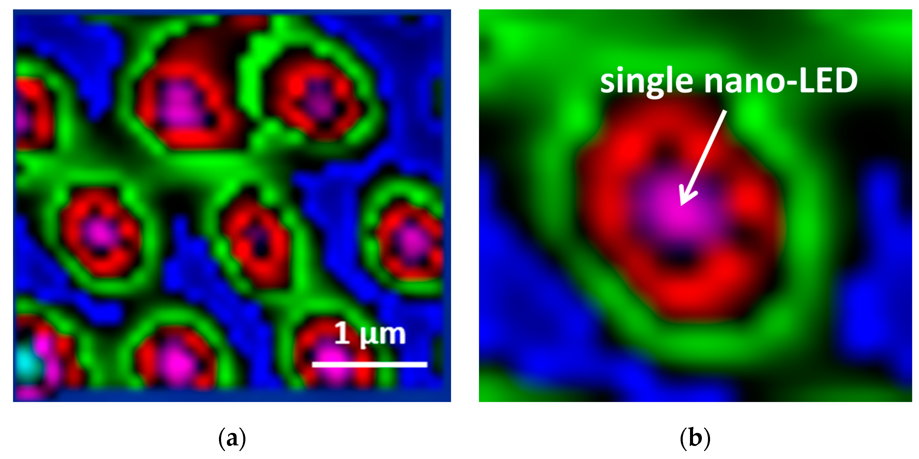
Figure 6.
(a) Micro-PL mapping from the single nano-LEDs in the array. Three different luminescence bands/maxima were observed previously [60] and are presented here graphically in colors. They are attributed to GaN band edge luminescence (blue), radiative recombination from the multi quantum well region with the emission maxima in the PL spectra at ~440–445 nm (pink/violet color) and defect luminescence ~540–600 nm (green-red). The etching process is responsible for the suppression of radiative recombination from the MQW region. (b) Detail of micro PL mapping for a single nano-LED structure without the injected nanocrystal-polymer suspension.

Figure 7.
(a) Detail-SEM image of the vertical hybrid-nano-LED device—aperture filled with injected polymer-nanocrystal suspension; (b) example for a hybrid nano-LED array. The hybrid nano-LEDs are singularly addressable by the respective “word” (grey) and “bit” lines (gold). Please note that “word” and “bit” lines in this image are colored for the sake of increasing the respective structure’s visibility.

Disclaimer/Publisher’s Note: The statements, opinions and data contained in all publications are solely those of the individual author(s) and contributor(s) and not of MDPI and/or the editor(s). MDPI and/or the editor(s) disclaim responsibility for any injury to people or property resulting from any ideas, methods, instructions or products referred to in the content. |
© 2024 by the authors. Licensee MDPI, Basel, Switzerland. This article is an open access article distributed under the terms and conditions of the Creative Commons Attribution (CC BY) license (https://creativecommons.org/licenses/by/4.0/).
Share and Cite
MDPI and ACS Style
Mikulics, M.; Winden, A.; Mayer, J.; Hardtdegen, H.H. Developments in Mask-Free Singularly Addressable Nano-LED Lithography. Nanomanufacturing 2024, 4, 99-110. https://doi.org/10.3390/nanomanufacturing4020007
AMA Style
Mikulics M, Winden A, Mayer J, Hardtdegen HH. Developments in Mask-Free Singularly Addressable Nano-LED Lithography. Nanomanufacturing. 2024; 4(2):99-110. https://doi.org/10.3390/nanomanufacturing4020007
Chicago/Turabian StyleMikulics, Martin, Andreas Winden, Joachim Mayer, and Hilde Helen Hardtdegen. 2024. "Developments in Mask-Free Singularly Addressable Nano-LED Lithography" Nanomanufacturing 4, no. 2: 99-110. https://doi.org/10.3390/nanomanufacturing4020007