Article

GaN-Based PCSS with High Breakdown Fields

1
Department of Electrical and Computer Engineering, Texas Tech University, Lubbock, TX 79409, USA
2
NessEngineering Inc., San Diego, CA 92196, USA
*
Author to whom correspondence should be addressed.
Electronics 2021, 10(13), 1600; https://doi.org/10.3390/electronics10131600
Submission received: 31 May 2021 / Revised: 29 June 2021 / Accepted: 1 July 2021 / Published: 3 July 2021

Abstract

:
The suitability of GaN PCSSs (photoconductive semiconductor switches) as high voltage switches (>50 kV) was studied using a variety of commercially available semi-insulating GaN wafers as the base material. Analysis revealed that the wafers’ physical properties were noticeably diverse, mainly depending on the producer. High Voltage PCSSs were fabricated in both vertical and lateral geometry with various contacts, ohmic (Ti/Al/Ni/Au or Ni/Au), with and without a conductive n-GaN or p-type layer grown by metal-organic chemical vapor deposition. Inductively coupled plasma (ICP) reactive ion etching (RIE) was used to form a mesa structure to reduce field enhancements allowing for a higher field to be applied before electrical breakdown. The length of the active region was also varied from a 3 mm gap spacing to a 600 µm gap spacing. The shorter gap spacing supports higher electric fields since the number of macro defects within the device’s active region is reduced. Such defects are common in hydride vapor phase epitaxy grown samples and are likely one of the chief causes for electrical breakdown at field levels below the bulk breakdown field of GaN. Finally, the switching behavior of PCSS devices was tested using a pulsed, high voltage testbed and triggered by an Nd:YAG laser. The best GaN PCSS fabricated using a 600 µm gap spacing, and a mesa structure demonstrated a breakdown field strength as high as ~260 kV/cm.

1. Introduction

PCSSs are a viable alternative to traditional vacuum or gas switches due to their high switching speed, reasonable lifetimes, and high electric field strength depending on the material. Such switches are capable of operating in two modes: (1) a linear “low-gain” mode where all carriers are supplied through photo-ionization and (2) a lock-on “high-gain” mode where the initial carriers are multiplied through an avalanche-like process. To operate in the lock-on mode, a minimum, material-dependent electric field must be applied across the switch, which was originally observed in high resistivity (semi-insulating) GaAs [1], as well as direct bandgap InP [2]. GaN as a direct bandgap semiconductor may be able to operate in either the linear or lock-on mode. Further acknowledging GaN’s wide bandgap (3.4 eV) and high nominal breakdown field (3.3 MV/cm) [3] make it a promising material for the fabrication of PCSSs. While the crystalline quality of GaN has significantly improved within the last few decades, undoped GaN is still nominally n-type with a relatively high free carrier concentration. Usually, Fe, C, or Mn are used as dopants in SI-GaN to compensate for these shallow donors [4]. Such SI-GaN has been proposed for a high breakdown field PCSS operating in the lock-in mode [5,6]. These wafers are commercially available from various vendors, including Kyma, Ammano, and Roditi. The optical, electrical, and morphological properties of these wafers were previously studied by the authors and were determined to be suitable substrates for the fabrication of high breakdown PCSSs [6]. With proper fabrication to reduce the effect of field enhancements, such SI GaN may be able to sustain the high fields necessary to operate in the lock-on mode [7].
Devices were tested using the pulse generator shown in Figure 1. With this setup, an initial 300 ns pulse is generated that is then amplified and stepped up to a maximum of ~58 kV by a 1:12 pulse transformer charging a transmission line through a series of stacked diodes. A 7 ns FWHM Nd:YAG laser is then used to trigger the device 200 ns after the pulse starts, a self-breaking air spark gap is then used to discharge the switch ~50 µs after the voltage is applied to prevent the voltage from being applied across the PCSS for an extended time. More details can be found in Ref. [8].

2. Processing

The switches were fabricated on 10 × 10 mm2 square SI-GaN (0001) wafers using several different processing techniques. Low contact resistivity n-GaN layers were selectively grown on SI-GaN wafers by metal-organic chemical vapor deposition (MOCVD) using a SiO2 mask grown by plasma-enhanced chemical vapor deposition (PCVD) [9]. P-type layers were also grown by MOCVD then patterned using ICP/RIE etching. Metal contacts were then deposited using a resist mask patterned with standard optical lithography and e-beam deposition of Ti, Al, Ni, and Au layers. A final 1 µm thick Au contact cap was sputtered before removing the resist. The contacts were then annealed in N2 for 110 s at 500 °C. Plasma etching techniques were also used to form a mesa structure. All etching was performed using a Cl2 based ICP/RIE system using 200 W ICP, 200 W RIE, 15/3/15 SCCM of Cl2/BCl3/Ar, respectively, and 30 mTorr. After fabrication, the samples were mounted on a PCB, and wire bonding was used to connect the switch to the PCB. The switches were then covered in a dielectric encapsulant to prevent surface flashover.

3. Design

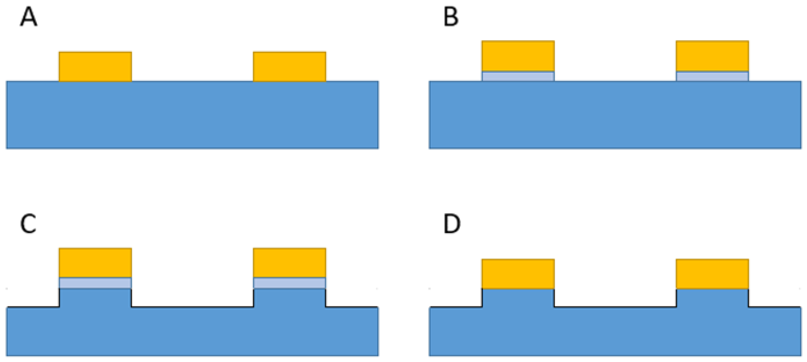
Initial switches were fabricated using a Ti/Al/Ti/Au stack to form ohmic contacts on the bulk SI:GaN, as shown in Figure 2A. These contacts were 2 × 2 mm2 arranged in a square pattern with a 3 mm gap between adjacent contacts allowing for up to four current pathways to be tested per device. Defining the average field amplitude as the quotient of applied voltage and gap size, it was found that switches fabricated in such a geometry have a breakdown average field strength of ~130 kV/cm. This is much lower than the 3.3 MV/cm breakdown field strength of GaN [3], suggesting that a significant field enhancement exists likely at the “triple point” where the GaN, metal contacts, and insulating material meet. Hence, a variety of switch geometries and contacts were implemented to reduce this field enhancement effect. A conductive n-type or p-type GaN layer was added under the metal contacts shown in Figure 2B. This layer helps to reduce the overall contact resistance and assists in lowering the current crowding effect at the edge of the contacts. Using these contacts, a roughly 15% improvement in the breakdown field was observed, with devices holding off fields up to 150 kV/cm.
Adding to the conductive layer, ICP/RIE etching was utilized to form a 1 µm high mesa around the contact, see Figure 2C. This mesa structure was believed to reduce field enhancements at the contact edges. Such etching also removed a layer with elevated impurity concentrations from the active region of the switches. This layer was observed in the SIMS profiles and is limited to approximately the top 700 nm of the wafers [6]. Switches fabricated using such a mesa along with a conductive GaN layer exhibited improved breakdown fields up to ~175 kV/cm.
A modified lateral switch layout was also implemented using the same structure as in Figure 2A, however, with a much smaller gap of 600 µm between the metal contacts. Assuming that there is a roughly constant number of defects per volume in the GaN material, the smaller gap also results in a smaller absolute number of defects, and it was thus possible to charge the devices to higher fields. Ultimately, a 50% increase in the breakdown field was found with ~200 kV/cm.
Finally, mesa etching was also applied to switches with a 600 µm gap spacing shown in Figure 2D. For such samples, no conductive layer was used as it was thought to have less impact on the etched samples. The addition of mesa etching improved the average breakdown field by 100% over the basic 3 mm geometry to ~260 kV/cm.

4. Discussion

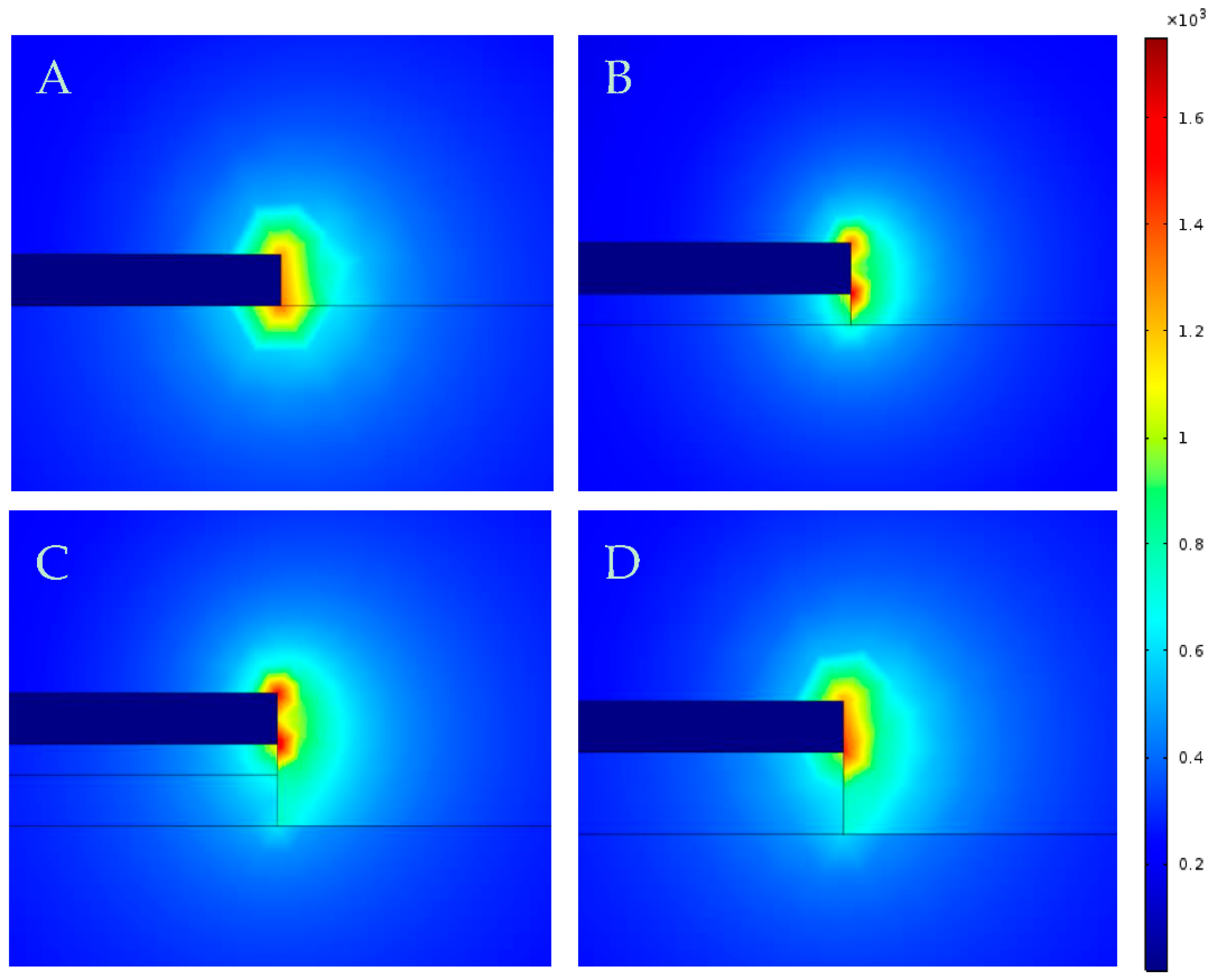
All PCSSs tested experienced breakdown at average electric fields on the order of 100 kV/cm. This is much lower than the expected 3.3 MV/cm breakdown field of GaN, and an indication of large field enhancements likely at the contact edges. Electric field simulations were performed using COMSOL for all geometries and are summarized in Figure 3. Samples fabricated using only metal contacts displayed the highest field enhancements with peak fields of ~16.5 times the applied average field within the GaN, shown in Figure 3A. Such switches experienced breakdown at ~130 kV/cm. From the simulation, it is thought to have had a peak field of ~2.1 MV/cm, which triggered a breakdown within the GaN. This is much more in line with the 3.3 MV/cm nominal breakdown field expected of GaN. A summary of the testing results along with simulated peak fields within the GaN can be seen in Table 1.
The addition of a conductive layer of GaN, shown in Figure 3B, reduced the peak electric field within the GaN. While there is still a notable field enhancement near the contact edges, the stressed volume is small as the enhancement is mainly confined to the dielectric near the contacts. The peak electric field was ~13.7 times the applied average field. Again, this implies a peak field within the GaN of ~2.1 MV/cm during breakdown. Mesa etching of the switches also helped to reduce the field enhancement, shown in Figure 3C. The peak electric field of the mesa switches was ~12.5 times the applied average field. With an average breakdown field of ~260 kV/cm, the associated peak field at breakdown is estimated from the simulation to be ~2.9 MV/cm.
The switches fabricated with a shorter 600 µm gap spacing demonstrated significantly higher breakdown fields than the 3 mm gap switches, which is likely due to fewer macro defects present in the active area of the switch and along the contact edges. Such macro defects are common in HVPE-grown bulk GaN. Initial 600 µm switches with only metal contacts experienced breakdown at an average field of ~200 kV/cm; this corresponds to a peak field of ~3.2 MV/cm.
Simulations also revealed that mesa etched switches with a conductive GaN layer greatly reduce the field enhancements within the bulk GaN. However, there is significant field enhancement within the conductive layer. The field enhancement is even higher than that for mesa-etched samples without a conductive layer. As such, the final 600 µm gap samples fabricated used a mesa structure without a conductive layer. The peak field within these samples was ~11.3 times the average field implying a peak field of ~2.9 MV/cm at an average breakdown field of ~260 kV/cm. The addition of the mesa structure in such samples greatly reduced the field enhancements of the switch. The peak field applied, however, was slightly reduced. This is believed to be the result of damage to the surface of the GaN following plasma etching.
Overall, the mesa structure performed the best, with the 3 mm switch holding off voltages up to 52.5 kV, while the 600 μm gap switch came experimentally closest to the intrinsic breakdown field level of GaN.

5. Conclusions

Bulk GaN PCSSs were fabricated with a variety of geometries to increase the average electric field that may be applied across the switch before electrical breakdown. Such geometries serve to reduce electric field enhancements in the GaN at the triple point, where the GaN, contact, and epoxy intersect. A shorter active region of the device was found to improve the breakdown field, which is thought to be due to a reduced number of macro defects within the switch. Conductive GaN layers may be added to improve unetched switches. However, this was found to be unnecessary when using a mesa structure to reduce field enhancements. Bulk GaN PCSSs were successfully fabricated to operate at high electric fields before breakdown at ~260 kV/cm. The bulk SI-GaN used for the switches was found to have had a maximum peak applied field of ~3.2 MV/cm at breakdown, which is close to the 3.3 MV/cm breakdown field of GaN.

Author Contributions

Conceptualization, A.N. and R.N.; software, M.G.; validation, M.G., V.K. and N.W.; formal analysis, S.N.; investigation, M.G.; writing—original draft preparation, M.G.; writing—review and editing, S.N. and A.N.; supervision, S.N.; project administration, A.N. All authors have read and agreed to the published version of the manuscript.

Funding

M.G. acknowledges the partial support from the grant #P200A 180068, from the US Department Education in the program of Graduate Assistance in the National Need (GAANN).

Data Availability Statement

Data available on request due to privacy restrictions.

Conflicts of Interest

The authors declare no conflict of interest.

References

  1. Loubriel, G.M.; Zutavern, F.J.; Hjalmarson, H.P.; O’Malley, M.W. Closing photoconductive semiconductor switches. In Proceedings of the 7th Pulsed Power Conference, Monterey, CA, USA, 11–14 June 1989; pp. 365–367. [Google Scholar]
  2. Zutavern, F.J.; Loubruel, G.M.; O′Malley, M.W.; Shanwald, L.P.; Helgeson, W.D.; McLaughlin, D.L.; McKenzie, B.B. Photoconductive semiconductor switch experiments for pulsed power applications. IEEE Trans. Electron Devices 1990, 37, 2472–2477. [Google Scholar] [CrossRef]
  3. Rais-Zadeh, M.; Gokhale, V.J.; Ansari, A.; Faucher, M.; Théron, D.; Cordier, Y.; Buchaillot, L. Gallium Nitride as Electromechanical material. J. Microelectromech. Syst. 2014, 23, 1252–1271. [Google Scholar] [CrossRef]
  4. Iwinska, M.; Zajac, M.; Lucznik, B.; Fijalkowski, M.; Amilusik, M.; Sochacki, T.; Litwin-Staszewska, E.; Piotrzkowski, R.; Grzegory, I.; Bockowski, M. Iron and manganese as dopants used in the crystallization of highly resistive HVPE-GaN on native seeds. Jpn. J. Appl. Phys. 2019, 58, SC1047. [Google Scholar] [CrossRef]
  5. Mar, A.; Hirsch, E.; Zutavern, F.; Pickrell, G.; Delhotal, J.; Gallegos, R.; Bigman, V.; Struve, K.; Teague, J.; Lehr, J.; et al. High-Gain Persistent Nonlinear Conductivity in High-Voltage Gallium Nitride Photoconductive Switches. In Proceedings of the 2018 IEEE International Power Modulator and High Voltage Conference, Jackson, WY, USA, 3–7 June 2018. [Google Scholar]
  6. Gaddy, M.; Kuryatkov, V.; Meyers, V.; Mauch, D.; Dickens, J.; Neuber, A.; Nikishin, S. Structural, morphological, optical and electrical properties of bulk (0001) GaN:Fe wafers. MRS Adv. 2018, 3, 179–184. [Google Scholar] [CrossRef]
  7. Chowdhury, A.R.; Nikishin, S.; Dickens, J.; Neuber, A.; Joshi, R.P.; Ness, R. Numerical srudies into the parameter space conductive to “lock-on” in a GaN photoconductive switch for high power applications. IEEE Trans. Dielectr. Electr. Insul. 2019, 26, 469. [Google Scholar] [CrossRef]
  8. Meyers, V.; Mauch, D.; Kuryatkov, V.; Nikishin, S.; Dickens, J.; Neuber, A.; Ness, R. Toward the development of an efficient bulk semi-insulating GaN photoconductive switch. In Proceedings of the 2017 IEEE 21st International Conference on Pulsed Power, Brighton, UK, 18–22 June 2017. [Google Scholar]
  9. Fen, W.; Kuryatkov, V.; Nikishin, S.; Holtz, M. Selective area epitaxy of InGaN quantum well triangular microrings with a single type of sidewall facets. J. Cryst. Growth 2010, 312, 1717–1720. [Google Scholar]
Figure 1. Electrical schematic diagram of pulse charging PCSS testbed (PCB). C10—energy storage capacitor, R13—current limiting resistor, X1—thyristor switch, TX3—step-up transformer with estimated parasitic capacitances C11, C12; L1—parasitic inductance; C8—pulse charged capacitance; R14—bleed resistor; U5, U7—behavior model of PCSS (closing and opening switch action); C9—parasitic load capacitance; R10—50 Ohm resistive load.
Electronics 10 01600 g001
Figure 2. A cross-sectional view of lateral PCSS fabricated with (A) metal contacts, (B) a conductive GaN layer and metal contacts, (C) a conductive GaN layer and metal contacts with a mesa etched profile, (D) metal contacts with a mesa etched profile.
Electronics 10 01600 g002
Figure 3. Electric field simulation results for lateral PCSS design showing field enhancements when charged to 100 kV/cm for (A) metal contacts, (B) a conductive GaN layer, (C) a conductive GaN layer and mesa etched profile, and (D) mesa etched profile.
Electronics 10 01600 g003
Table 1. Summary of testing results for all geometries and the simulated peak electric field at breakdown.
Sample GeometryGap SpacingApplied VoltageAverage FieldSimulated Peak Field
Metal Contacts3 mm39 kV~130 kV/cm~2.1 MV/cm
Conductive GaN Layer3 mm45 kV~150 kV/cm~2.1 MV/cm
Conductive GaN Layer with Mesa3 mm52.5 kV~175 kV/cm~2.2 MV/cm
Metal Contacts600 µm12.2 kV~200 kV/cm~3.2 MV/cm
Mesa600 µm15.6 kV~260 kV/cm~2.9 MV/cm
Publisher’s Note: MDPI stays neutral with regard to jurisdictional claims in published maps and institutional affiliations.