
Fabrication of a UV Photodetector Based on n-TiO2/p-CuMnO2 Heterostructures


 ,
, 
Abstract
:1. Introduction
2. Materials and Methods
2.1. Reagents
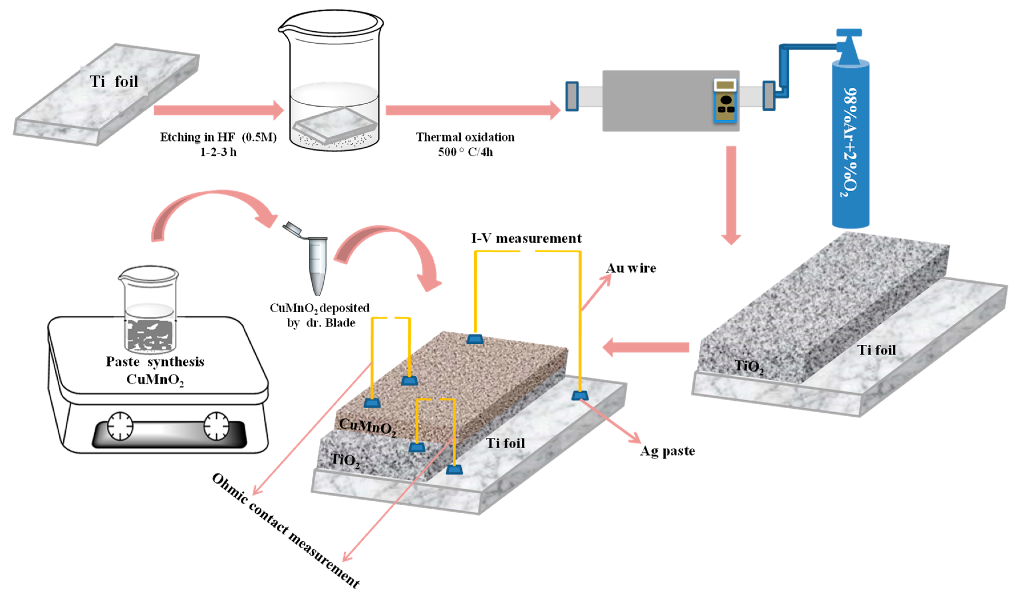
2.2. Fabrication of the Sensors Based on the “n-p” Type Heterojunction Ti-TiO2-CuMnO2
2.3. Materials Characterization
3. Results and Discussion
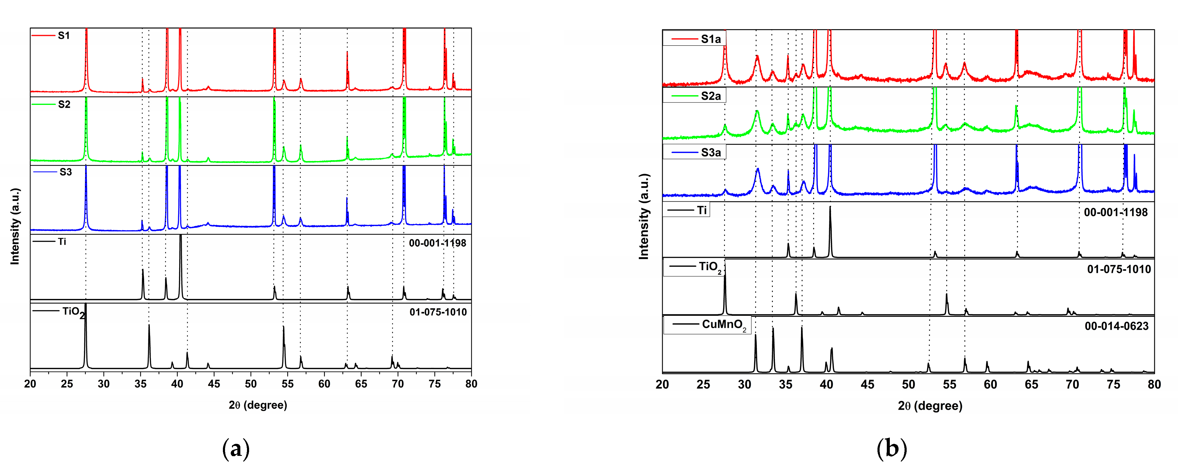
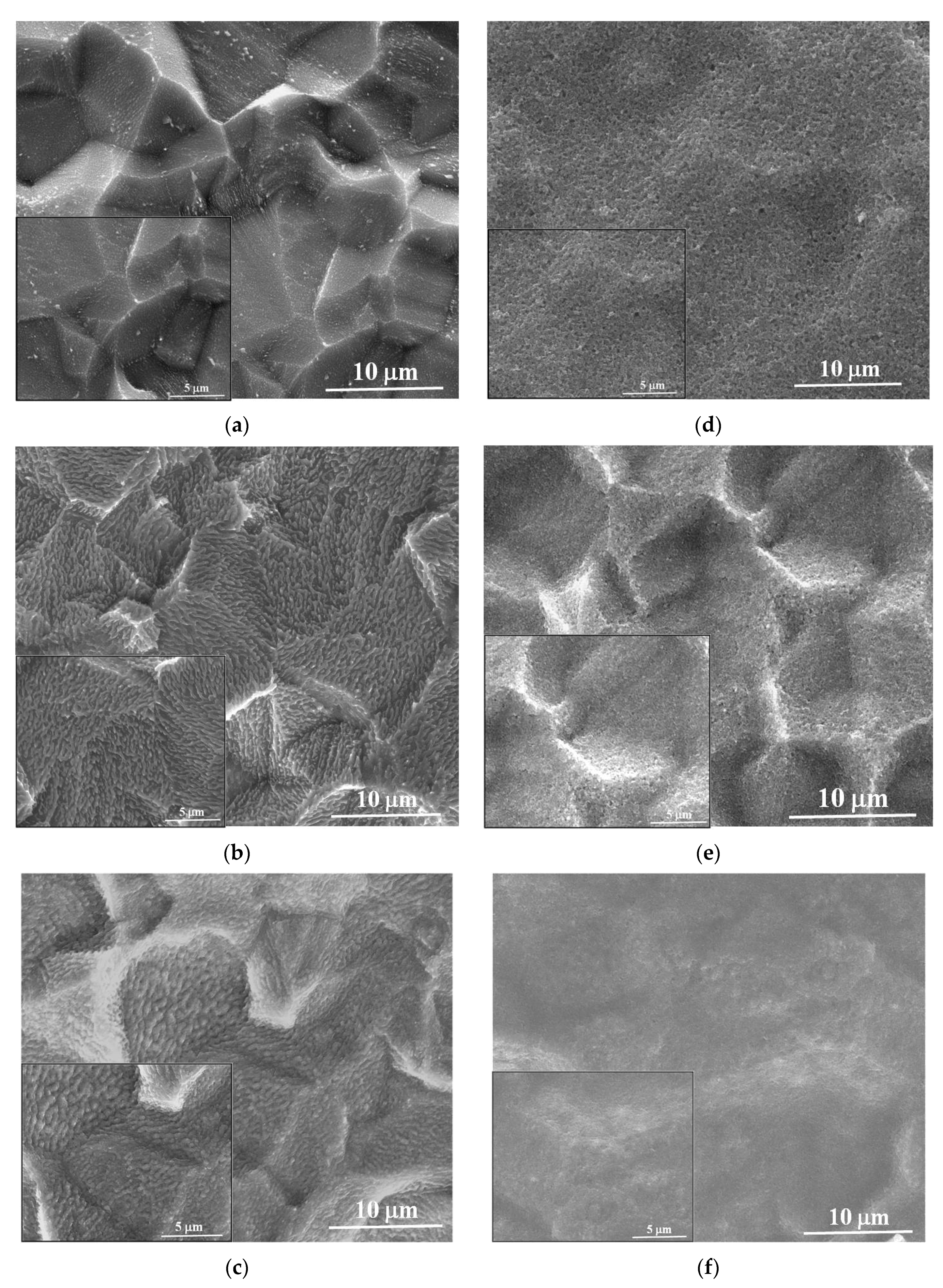
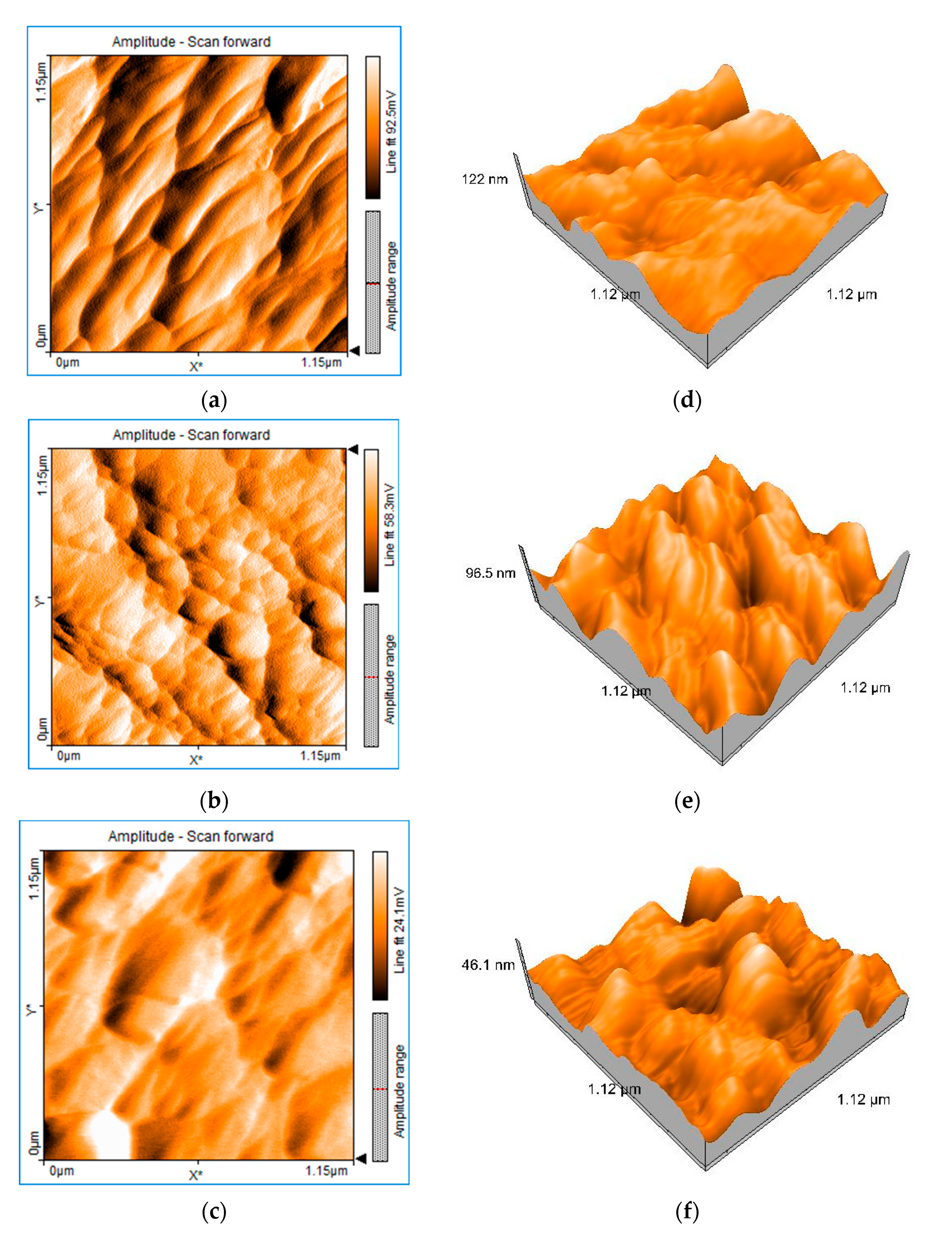
3.1. Structural and Morphological Characteristics
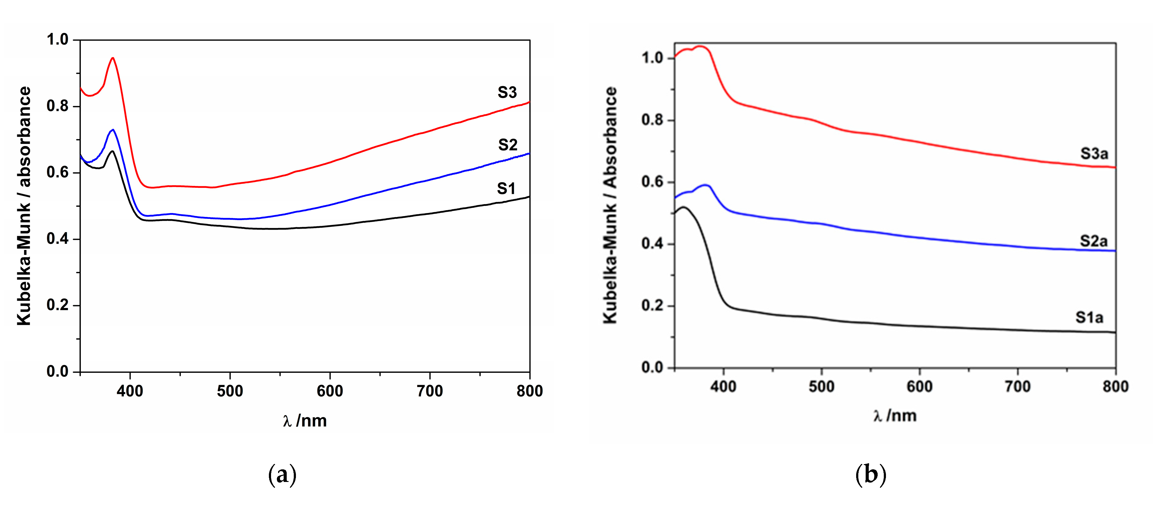
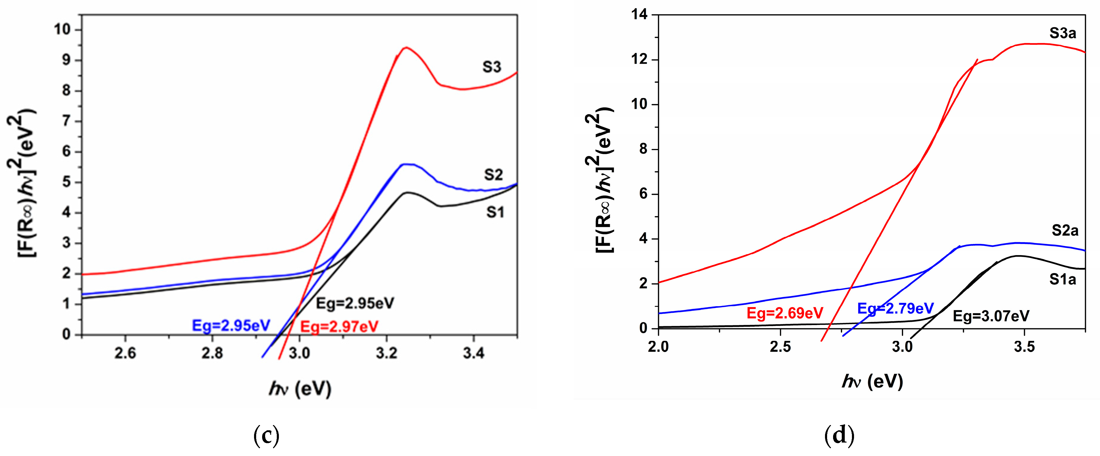
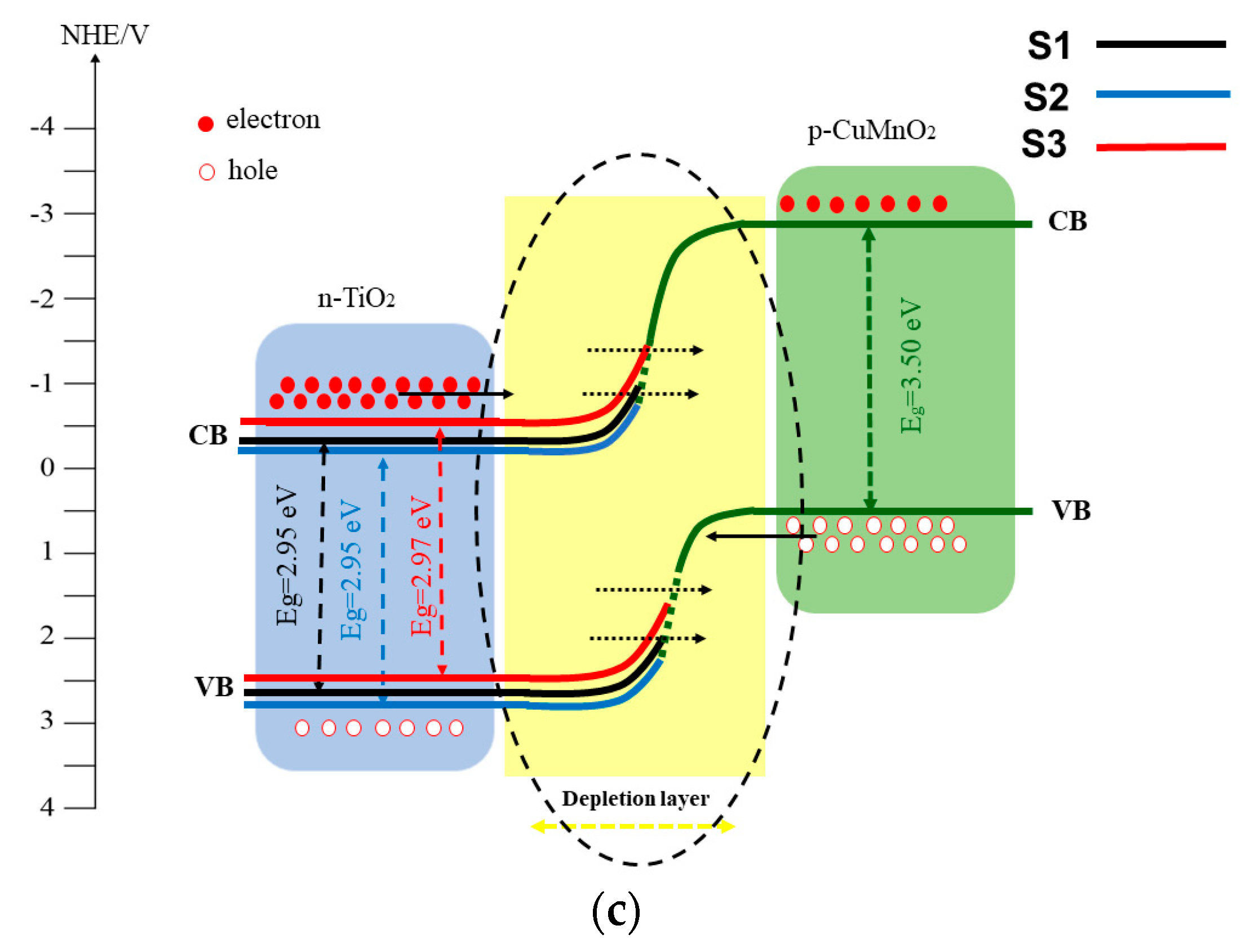
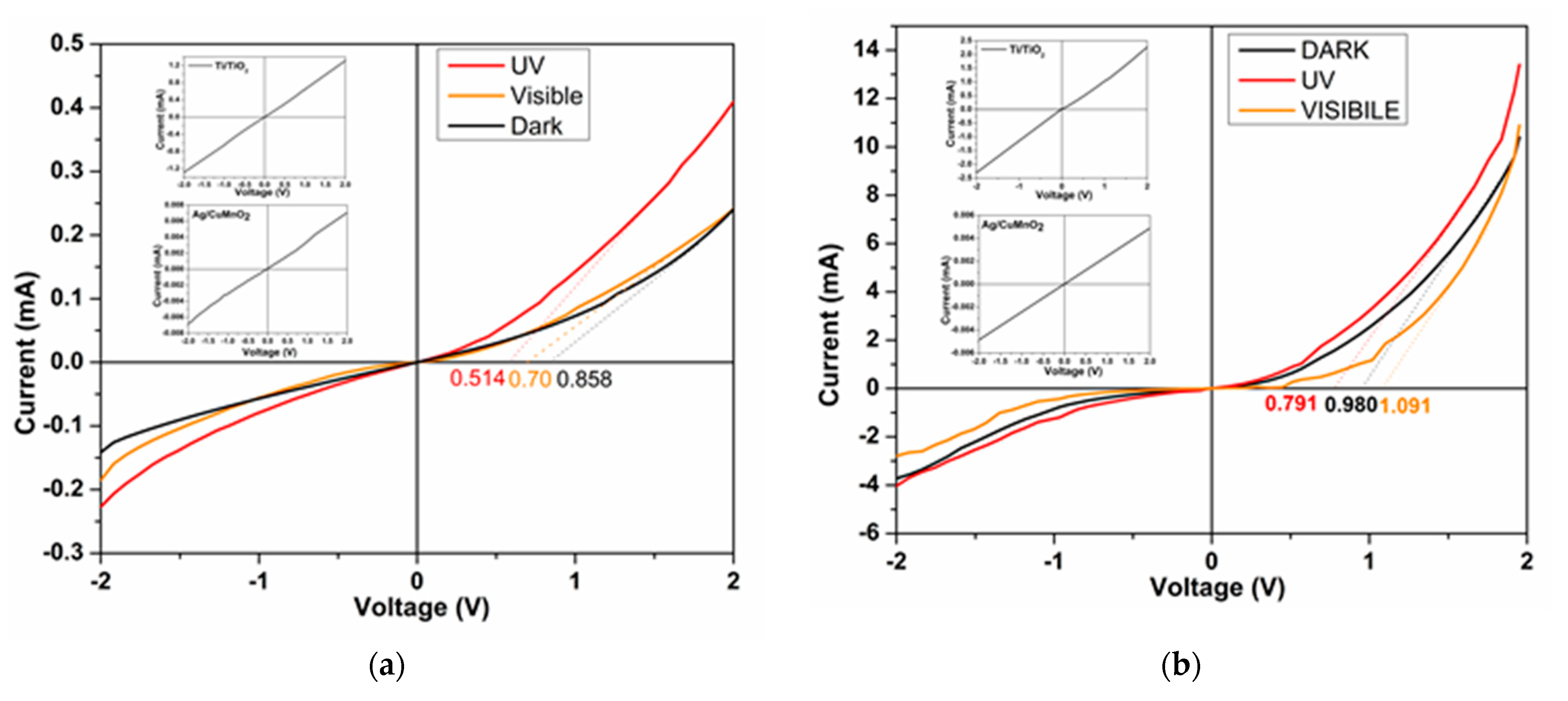
3.2. Optical, Electrochemical and Electrical Properties
4. Conclusions
Author Contributions
Funding
Institutional Review Board Statement
Informed Consent Statement
Data Availability Statement
Acknowledgments
Conflicts of Interest
References
- Nunes, D.; Pimente, A.; Gonçalves, A.; Pereira, S.; Branquinho, R.; Barquinha, P.; Fortunato, E.; Martins, R. Metal Oxide Nanostructures for Sensor Applications. Semicond. Sci. Technol. 2019, 34, 1–178. [Google Scholar] [CrossRef] [Green Version]
- Sun, X.; Azad, F.; Wang, S.; Zhao, L.; Su, S. Low-cost flexible ZnO microwires array ultraviolet photodetector embedded in PAVL substrate. Nanoscale Res. Lett. 2018, 13, 277–285. [Google Scholar] [CrossRef] [PubMed]
- Xie, Y.; Wei, L.; Wei, G.; Li, Q.; Jiao, J. A self-powered UV photodetector based on TiO2 nanorod arrays. Nanoscale Res. Lett. 2013, 8, 188–194. [Google Scholar] [CrossRef] [Green Version]
- Ji, Y.; Jung, U.; Xian, Z.; Kim, D.; Yu, J.; Park, J. Ultraviolet photodetectors using hollow p-CuO nanospheres/n-ZnO nanorods with a pn junction structure. Sens. Actuators B Chem. 2020, 304, 111876–111883. [Google Scholar] [CrossRef]
- Wei, T.; Chao, Z.; Tianyou, Z.; Song-Lin, L.; Xi, W.; Meiyong, L.; Kazuhito, T.; Dmitri, G.; Yoshio, B. Flexible SnO2 hollow nanosphere film based high performance ultraviolet photodetector. Chem. Commun. 2013, 49, 3739–3741. [Google Scholar]
- Jiang, W.; Zheng, T.; Wu, B.; Jiao, H.; Wang, X.; Chen, Y.; Zhang, X.; Peng, M.; Wang, H.; Lin, T.; et al. A versatile photodetector assisted by photovoltaic and bolometric effects. Light Sci. Appl. 2020, 9, 160–169. [Google Scholar] [CrossRef]
- Jia, M.; Wang, F.; Tang, L.; Xiang, J.; Teng, K.S.; Lau, S.P. High-Performance Deep Ultraviolet Photodetector Based on NiO/β-Ga2O3 Heterojunction. Nanoscale Res. Lett. 2020, 15, 47–53. [Google Scholar] [CrossRef] [Green Version]
- Talebian, N.; Nilforoushan, M.R. Comparative study of the structural, optical and photocatalytic properties of semiconductor metal oxides toward degradation of methylene blue. Thin Solid Films. 2010, 518, 2210–2215. [Google Scholar] [CrossRef]
- Xin, X.; Scheiner, M.; Ye, M.; Lin, Z. Surface-treated TiO2 nanoparticles for dye-sensitized solar cells with remarkably enhanced performance. Langmuir 2011, 27, 14594–14598. [Google Scholar] [CrossRef]
- Gholami, M.; Bahar, M.; Azim-Araghi, M.E. The preparation of TiO2 nanoparticles and investigation of its electrical properties as CO2 gas sensor at room temperature. Chem. Phys. Lett. 2012, 48, 9626–9628. [Google Scholar]
- Sarkar, S.; Das, R.; Choi, H.; Bhattacharjee, C. Involvement of process parameters and various modes of application of TiO2 nanoparticles in heterogeneous photocatalysis of pharmaceutical wastes—A short review. R. Soc. Chem. 2014, 4, 57250–57266. [Google Scholar] [CrossRef]
- Nakata, K.; Fujishima, A. TiO2 photocatalysis: Design and applications. J. Photochem. Photobiol. C Photochem. Rev. 2012, 13, 169–189. [Google Scholar] [CrossRef]
- Zu, G.; Li, H.; Liu, S.; Li, D.; Wang, J.; Zhao, J. Highly efficient mass determination of TiO2 nanotube arrays and its application in lithium-ion batteries. Sustain. Mater. Technol. 2018, 18, 79–104. [Google Scholar] [CrossRef]
- Kargan, N.H.; Aliahmad, M.; Azizi, S. Detecting Ultra-Violet Radiation by Using Titanium Dioxide Nanoparticles, Soft Nanoscience. Letters 2012, 2, 29–33. [Google Scholar]
- Nayef, U.M.; Hubeatir, K.A.; Abdulkareem, Z.J. Ultraviolet Photodetector based on TiO2 Nanoparticles/Porous Silicon Hetrojunction. Optik 2016, 127, 2806–2810. [Google Scholar] [CrossRef]
- Nunes, D.; Pimentel, A.; Araujo, A.; Calmeiro, T.R.; Panigrahi, S.; Pinto, J.V.; Barquinha, P.; Gama, M.; Fortunato, E.; Martins, R. Enhanced UV Flexible Photodetectors and Photocatalysts Based on TiO2 Nanoplatforms. Top. Catal. 2018, 61, 1591–1606. [Google Scholar] [CrossRef] [Green Version]
- Gao, P.; Ma, H.; Yan, T.; Wu, D.; Ren, X.; Yang, J.; Du, B.; Wei, Q. Construction of dentate bonded TiO2-CdSe heterostructures with enhanced photoelectrochemical properties: Versatile labels toward photoelectrochemical and electrochemical sensing. Dalton Trans. 2015, 44, 773–781. [Google Scholar] [CrossRef] [PubMed]
- Sun, M.; Hu, J.; Zhai, C.; Zhu, M.; Pan, J. A p-n heterojunction of CuI/TiO2 with enhanced photoelectrocatalytic activity for methanol electro-oxidation. Electrochim. Acta 2017, 245, 863–871. [Google Scholar] [CrossRef]
- Wang, Y.; Zhang, Y.; Zhao, G.; Tian, H.; Shi, H.; Zhou, T. Design of a Novel Cu2O/TiO2/Carbon Aerogel Electrode and Its Efficient Electrosorption-Assisted Visible Light Photocatalytic Degradation of 2,4,6-Trichlorophenol. ACS Appl. Mater. Interfaces 2012, 4, 3965–3972. [Google Scholar] [CrossRef] [PubMed]
- Li, Y.; Cai, C.; Gu, Y.; Cheng, W.; Xiong, W.; Zhao, C. Novel electronic properties of a new MoS2/TiO2 heterostructure and potential applications in solar cells and photocatalysis. Appl. Surf. Sci. 2017, 414, 34–40. [Google Scholar] [CrossRef]
- Zhang, D.; Gu, X.; Jing, F.; Gao, F.; Zhou, J.; Ruan, S. High performance ultraviolet detector based on TiO2/ZnO heterojunction. J. Alloys Compd. 2015, 618, 551–554. [Google Scholar] [CrossRef]
- Shi, J.; Liang, H.; Xia, X.; Abbas, Q. Band alignment analysis of CuGaO2/β-Ga2O3 heterojunction and application to deep-UV photodetector. Appl. Surf. Sci. 2021, 569, 151010. [Google Scholar] [CrossRef]
- Ahmadi, M.; Abrari, M.; Ghanaatshoar, M. An all-sputtered photovoltaic ultraviolet photodetector based on co-doped CuCrO2 and Al-doped ZnO heterojunction. Nature 2021, 11, 18694. [Google Scholar] [CrossRef]
- Dursun, S.; Kaya, I.C.; Kalem, V.; Akyildiz, H. UV/Visible Light Active CuCrO2 Nanoparticle-SnO2 Nanofiber p-n Heterostructured Photocatalyst for Photocatalytic Applications. Dalton Trans. 2018, 47, 14662–14678. [Google Scholar] [CrossRef] [PubMed]
- Velmurugan, S.; Zhi-Xiang, L.; Yang, T.C.-K.; Juan, J.C. Rational design of built-in stannic oxide-copper manganate microrods p-n heterojunction for photoelectrochemical sensing of tetracycline. Chemosphere 2021, 271, 129788–129800. [Google Scholar] [CrossRef]
- Lazau, C.; Poienar, M.; Orha, C.; Ursu, D.; Nicolaescu, M.; Vajda, M.; Bandas, C. Development of a new “n-p” heterojunction based on TiO2 and CuMnO2 synergy materials. Mater. Chem. Phys. 2021, 272, 124999–125008. [Google Scholar] [CrossRef]
- Tsai, T.Y.; Chang, S.J.; Hsueh, T.J.; Hsueh, H.T.; Weng, W.Y.; Hsu, C.L.; Dai, B.T. p-Cu2O-shell/n-TiO2-nanowires-corehetrostructure photodiodes. Nanoscale Res. Lett. 2011, 6, 575–581. [Google Scholar] [CrossRef] [Green Version]
- Wang, D.H.; Jia, L.; Wu, X.L.; Lu, L.Q.; Xu, A.W. One-step hydrothermal synthesis of N-doped TiO2/C nanocomposites with high visible light photocatalytic activity. Nanoscale Res. Lett. 2012, 4, 576–584. [Google Scholar] [CrossRef]
- Chang, Y.H.; Liu, C.M.; Chen, C.; Cheng, H.E. The heterojunction effects of TiO2 nanotubes fabricated by atomic layer deposition on photocarrier transportation direction. Nanoscale Res. Lett. 2012, 7, 231–238. [Google Scholar] [CrossRef] [PubMed] [Green Version]
- Hosseini, Z.S.; Shasti, M.; Sani, S.R.; Mortezaali, A. Photo-detector diode based on thermally oxidized TiO2 nanostructures/p-Si heterojunction. J. Appl. Phys. 2016, 119, 014503. [Google Scholar] [CrossRef]
- Desai, U.V.; Xu, C.K.; Wu, J.M.; Gao, D. Hybrid TiO2-SnO2 nanotube arrays for dye-sensitized solar cells. J. Phys. Chem. C 2013, 117, 3232–3239. [Google Scholar] [CrossRef]
- Khun, K.; Ibupoto, Z.H.; Willander, M. Development of fast and sensitive ultraviolet photodetector using p-type NiO/n-type TiO2 heterostructures. Phys. Status Solidi 2013, 210, 2720–2724. [Google Scholar] [CrossRef]
- Luo, J.S.; Ma, L.; He, T.C.; Ng, C.F.; Wang, S.J.; Sun, H.D.; Fan, H.J. TiO2/(CdS, CdSe, CdSes) nanorod heterostructures and photoelectrochemical properties. J. Phys. Chem. C 2012, 116, 11956–11963. [Google Scholar] [CrossRef]
- Pansri, S.; Supruangnet, R.; Nakajima, H.; Rattanasuporn, S.; Noothongkaew, S. Band offset determination of p-NiO/n-TiO2 heterojunctions for applications in high-performance UV photodetectors. J. Mater. Sci. 2020, 55, 4332–4344. [Google Scholar] [CrossRef]
- Singha, S.V.; Sharma, A.; Biring, S.; Pal, B.N. Solution processed Cu2S/TiO2 heterojunction for visible-near infrared photodetector. Thin Solid Films 2020, 710, 138275. [Google Scholar] [CrossRef]
- Poienar, M.; Lungu, A.; Sfirloaga, P.; Lungu, M.; Mihali, C.V.; Vlazan, P. Use of ultrasound-assisted co-precipitation route to obtain CuMnO2 semiconductor nanomaterials. Chem. Pap. 2019, 73, 1541–1546. [Google Scholar] [CrossRef]
- Skoneczny, W.; Niedźwiedź, M.; Bara, M. The Effect of production parameters of oxide layers on their nanostructure, nanomorphology, and surface free energy. Appl. Sci. 2018, 8, 2251–2262. [Google Scholar] [CrossRef] [Green Version]
- Birdeanu, A.-V.; Birdeanu, M.; Fagadar-Cosma, E. Corrosion protection characteristics of ceramics, porphyrins and hybrid ceramics/porphyrins, deposited as single and sandwich layers, by pulsed laser deposition (PLD). J. Alloy Compd. 2017, 706, 220–226. [Google Scholar] [CrossRef]
- AlShammari, A.S.; Halim, M.M.; Yam, F.K.; Kaus, N.H.M. Effect of precursor concentration on the performance of UV photodetector using TiO2/reduced graphene oxide (rGO) nanocomposite. Results Phys. 2020, 19, 103630. [Google Scholar] [CrossRef]
- Molina-Mendoza, A.J.; Moya, A.; Frisenda, R.; Svatek, A.S.; Gant, P.; Gonzalez-Abad, S.; Antolin, E.; Agraït, N.; Rubio-Bollinger, G.; Perez de Lara, D.; et al. Highly responsive UV-photodetectors based on single electrospun TiO2 nanofibres. J. Mater. Chem. C 2016, 4, 10707–10714. [Google Scholar] [CrossRef] [Green Version]
- Echresh, A.; Chey, C.O.; Zargar Shoushtari, M.; Khranovskyy, V.; Nur, O.; Willander, M. UV photo-detector based on p-NiO thin film/n-ZnO nanorods heterojunction prepared by a simple process. J. Alloy Compd. 2015, 632, 165–171. [Google Scholar] [CrossRef] [Green Version]
- Cossuet, T.; Resende, J.; Rapenne, L.; Chaix-Pluchery, O.; Jiménez, C.; Renou, G.; Pearson, A.J.; Hoye, R.L.Z.; Blanc-Pelissier, D.; Nguyen, N.D.; et al. ZnO/CuCrO2 Core-Shell nanowire heterostructures for self-powered UV photodetectors with fast response. Adv. Funct. Mater. 2018, 28, 1803142–1803154. [Google Scholar] [CrossRef]
- Mishra, M.; Gundimeda, A.; Garg, T.; Dash, A.; Das, S.; Vandana; Gupta, G. ZnO/GaN heterojunction based self-powered photodetectors: Influence of interfacial states on UV sensing. Appl. Surf. Sci. 2019, 478, 1081–1089. [Google Scholar] [CrossRef]
- Chen, L.; Honsho, Y.; Seki, S.; Jiang, D. Light-Harvesting Conjugated Microporous Polymers: Rapid and Highly Efficient Flow of Light Energy with a Porous Polyphenylene Framework as Antenna. J. Am. Chem. Soc. 2010, 132, 6742–6748. [Google Scholar] [CrossRef]
- Um, H.D.; Moiz, S.A.; Park, K.T.; Jung, J.-Y.; Jee, S.W.; Ahn, C.H.; Kim, D.C.; Cho, H.K.; Kim, D.-W.; Lee, J.-H. Highly selective spectral response with enhanced responsivity of n-ZnO/p-Si radial heterojunction nanowire photodiodes. Appl. Phys. Lett. 2011, 98, 033102. [Google Scholar] [CrossRef]
- Brötzmann, M.; Vetter, U.; Hofsäss, H. BN/ZnO heterojunction diodes with apparently giant ideality factors. J. Appl. Phys. 2009, 106, 063704. [Google Scholar] [CrossRef]
- Prabhu, R.R.; Saritha, A.C.; Shijeesh, M.R.; Jayara, M.K. Fabrication of p-CuO/n-ZnO heterojunction diode via sol-gel spin coating technique. Mater. Sci. Eng. B 2017, 220, 82–90. [Google Scholar] [CrossRef]
- Ranjith, K.S.; Kumar, R.T. Facile construction of vertically aligned ZnO nanorod/PEDOT:PSS hybrid heterojunction-based ultraviolet light sensors: Efficient performance and mechanism. Nanotechnology 2016, 27, 095304. [Google Scholar] [CrossRef] [PubMed]
- Sah, C.T.; Noyce, R.N.; Shockley, W. Carrier generation and recombination in pn junctions and pn junction characteristics. Proc. IRE 1957, 45, 1228–1243. [Google Scholar] [CrossRef]
- Mridha, S.; Ghosh, R.; Basak, D. Ultraviolet Photodetection Properties of a Pt Contact on a Mg0.1Zn0.9O/ZnO Composite Film. J. Electron. Mater. 2007, 36, 1643–1647. [Google Scholar] [CrossRef]
- Tyagi, M.; Tomar, M.; Gupta, V. Trap assisted space charge conduction in p-NiO/n-ZnO heterojunction diode. Mater. Res. Bull. 2015, 66, 123–131. [Google Scholar] [CrossRef]
- Qiao, B.; Zhang, Z.; Xie, X.; Li, B.; Li, K.; Chen, X.; Zhao, H.; Liu, K.; Liu, L.; Shen, D. Avalanche Gain in Metal-Semiconductor−Metal Ga2O3 Solar-Blind Photodiodes. J. Phys. Chem. C 2019, 123, 18516–18520. [Google Scholar] [CrossRef]
- Sarwar Rana, A.H.; Shaikh, S.F.; Al-Enizi, A.M.; Agyeman, D.A.; Ghani, F.; Nah, I.W.; Shahid, A. Intrinsic Control in Defects Density for Improved ZnO Nanorod-Based UV Sensor Performance. Nanomaterials 2020, 10, 142–158. [Google Scholar] [CrossRef] [PubMed] [Green Version]
- Velilla, E.; Cano, J.; Jimenez, K.; Valencia, J.; Ramirez, D.; Jaramillo, F. Numerical analysis to determine reliable one-diode model parameters for Perovskite solar cells. Energies 2018, 11, 1963. [Google Scholar] [CrossRef] [Green Version]
- Elsaeedy, H.I.; Qasem, A.; Yakout, H.A.; Mahmoud, M. The pivotal role of TiO2 layer thickness in optimizing the performance of TiO2/P-Si solar cell. J. Alloy Compd. 2021, 867, 159150–159163. [Google Scholar] [CrossRef]
- Chabri, S.; Dhara, A.; Show, B.; Adak, D.; Sinha, A.; Mukherjee, N. Mesoporous CuO-ZnO p-n heterojunction based nanocomposites with high specific surface area for enhanced photocatalysis and electrochemical sensing. Catal. Sci. Technol. 2016, 6, 3238–3252. [Google Scholar] [CrossRef]
- Rothschild, A.; Komem, Y. The effect of grain size on the sensitivity of nanocrystalline metal-oxide gas sensors. J. Appl. Phys. 2004, 95, 6374–6380. [Google Scholar] [CrossRef]
- Wang, C.; Yin, L.; Zhang, L.; Xiang, D.; Gao, R. Metal oxide gas sensors: Sensitivity and influencing factors. Sensors 2010, 10, 2088–2106. [Google Scholar] [CrossRef] [Green Version]


| Sample | Codes | Etching (Ti Foil) CHF(M)/t(h) | Oxidation T(°C)/t(h) | Sensor Type | Codes | Thermal Treatment T(°C)/t(h) | |
|---|---|---|---|---|---|---|---|
| Ti-TiO2 | S1 | 0.5 | 1 | 500/4 | Ti-TiO2-CuMnO2 | S1a | 250/1 |
| S2 | 2 | S2a | |||||
| S3 | 3 | S3a | |||||
| Sample | Etching Time (h) | Particle Size (nm) | Sa (nm) | Sq (nm) | Sp (nm) | Sv (nm) | Layer Thickness Sp-Sv (nm) [38] |
|---|---|---|---|---|---|---|---|
| S1 | 1 | 86 | 20.547 | 24.988 | 29.800 | −37.804 | 57.604 |
| S2 | 2 | 69 | 16.560 | 20.004 | 51.492 | −56.759 | 108.251 |
| S3 | 3 | 20 | 8.4521 | 10.758 | 104.64 | −76.487 | 181.127 |
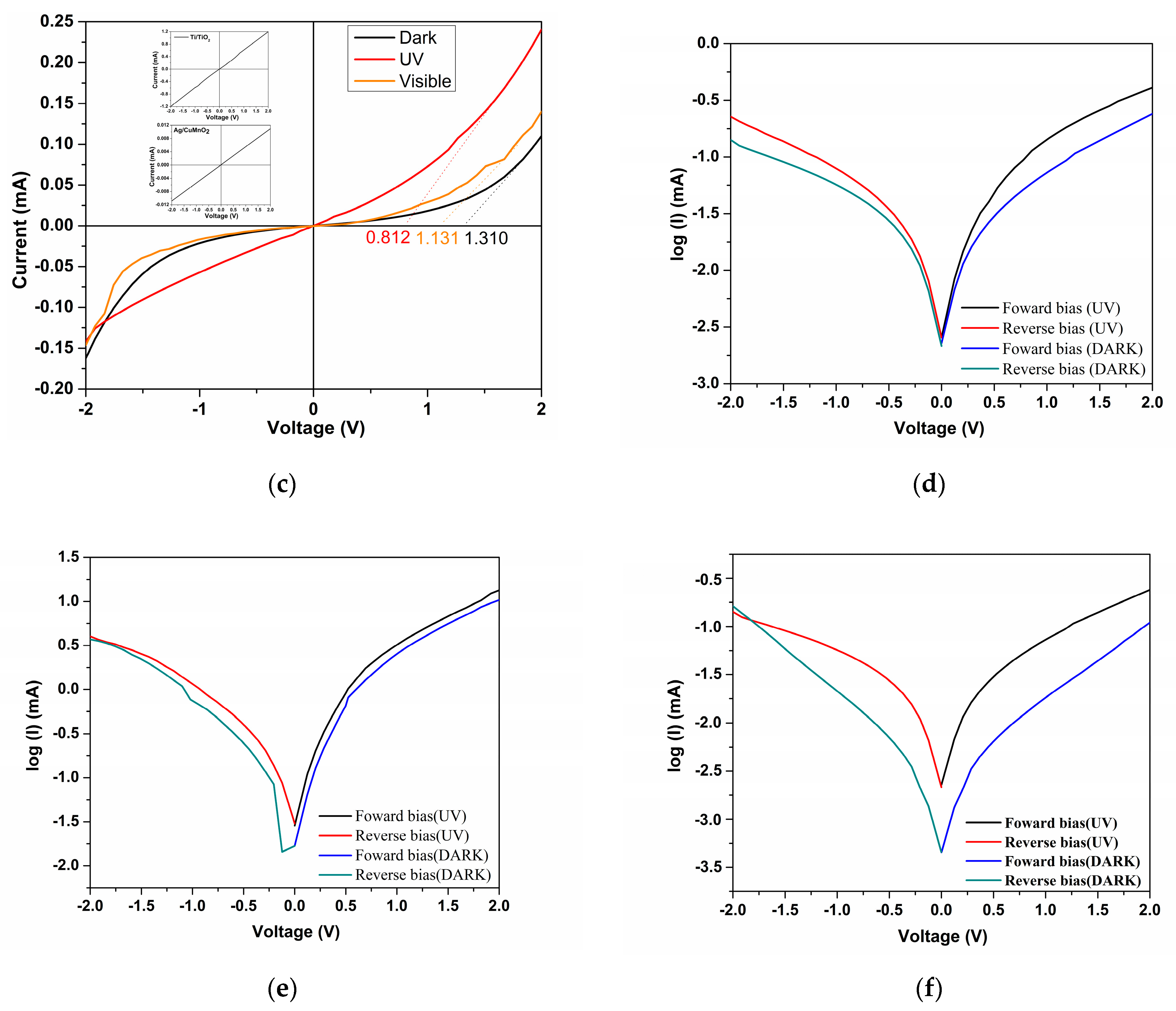
| Sample | Type | VT (V) | IF (A) | IR (A) | n | I0 (A) |
|---|---|---|---|---|---|---|
| S1a | Dark | 0.858 | 0.24 × 10⁻³ | 0.14 × 10⁻³ | 3.95 | 1.66 × 10⁻⁹ |
| UV | 0.513 | 0.41 × 10⁻³ | 0.22 × 10⁻³ | - | 1.82 × 10⁻⁹ | |
| S2a | Dark | 0.980 | 10 × 10−3 | 3 × 10⁻³ | 3.40 | 0.013 × 10⁻⁹ |
| UV | 0.791 | 13 × 10−3 | 4 × 10⁻³ | - | 0.025 × 10⁻⁹ | |
| S3a | Dark | 1.310 | 0.11 × 10⁻³ | 0.16 × 10⁻³ | 6.48 | 0.55 × 10⁻⁹ |
| UV | 0.812 | 0.24 × 10⁻³ | 0.14 × 10⁻³ | - | 3.93 × 10⁻⁹ |
Publisher’s Note: MDPI stays neutral with regard to jurisdictional claims in published maps and institutional affiliations. |
© 2021 by the authors. Licensee MDPI, Basel, Switzerland. This article is an open access article distributed under the terms and conditions of the Creative Commons Attribution (CC BY) license (https://creativecommons.org/licenses/by/4.0/).
Share and Cite
Nicolaescu, M.; Bandas, C.; Orha, C.; Şerban, V.; Lazău, C.; Căprărescu, S. Fabrication of a UV Photodetector Based on n-TiO2/p-CuMnO2 Heterostructures. Coatings 2021, 11, 1380. https://doi.org/10.3390/coatings11111380
Nicolaescu M, Bandas C, Orha C, Şerban V, Lazău C, Căprărescu S. Fabrication of a UV Photodetector Based on n-TiO2/p-CuMnO2 Heterostructures. Coatings. 2021; 11(11):1380. https://doi.org/10.3390/coatings11111380
Chicago/Turabian StyleNicolaescu, Mircea, Cornelia Bandas, Corina Orha, Viorel Şerban, Carmen Lazău, and Simona Căprărescu. 2021. "Fabrication of a UV Photodetector Based on n-TiO2/p-CuMnO2 Heterostructures" Coatings 11, no. 11: 1380. https://doi.org/10.3390/coatings11111380