Abstract
In this work, we describe the role of the different layers in perovskite solar cells to achieve reproducible, ~16% efficient perovskite solar cells. We used a planar device architecture with PEDOT:PSS on the bottom, followed by the perovskite layer and an evaporated C60 layer before deposition of the top electrode. No high temperature annealing step is needed, which also allows processing on flexible plastic substrates. Only the optimization of all of these layers leads to highly efficient and reproducible results. In this work, we describe the effects of different processing conditions, especially the influence of the C60 top layer on the device performance.
1. Introduction
Perovskite solar cells have attracted a lot of attention since their first report in 2009 [1]. Within five years, the reported efficiency has exceeded over 20% [2,3], which makes it an extremely promising and fast developing candidate for a next generation solar cell. This exciting progress is attributed to the application and exploration of organic-inorganic lead-halide perovskite. Perovskite is a large class of materials, named after the Russian mineralogist Lev Perovski. This special lead-halide perovskite possesses almost all desired properties for light-harvesting solar cell materials, such as suitable direct band-gap [4,5,6,7], strong light absorption ability [8,9], long charge carrier diffusion length [10,11,12,13] and so on. It is exceptional that it forms an excellent light harvesting semiconductor material from solution processing.
Perovskite solar cells were first fabricated using dye-sensitized solar cell architecture with the perovskite as a thin absorber layer on top of a mesoporous TiO2 electron acceptor layer [14,15,16]. Soon, it became clear that the mesoporous TiO2 is not needed for charge separation as exciton binding energy in perovskites is very low (comparable to inorganic semiconductors) and charge diffusion lengths for electrons and hole are large and relatively balanced [12,13]. Consecutively, planar n-i-p perovskite solar cell architectures have successfully been fabricated [17,18,19]. However, in the two types of architecture above, the high temperature sintering process of the TiO2 film (mesoporous or planar) and serious hysteresis behavior [20,21,22,23] have become an obstacle to potential commercial application.
In contrast, an inverted perovskite p-i-n planar heterojunction can be fabricated by a low-temperature process when using poly-(2,3-dihydrothieno-1,4-dioxin)–poly(styrene -sulfonate) (PEDOT:PSS) and C60 as hole and electron extraction layers. Such cells are compatible with commercial roll-to-roll fabrication techniques also on flexible substrates, and the hysteresis phenomenon is also greatly suppressed in this cell layout [24,25,26,27,28]. Therefore, a lot of efforts have been focused on achieving the full potential of p-i-n type perovskite solar cells. Several film deposition methods have been used to fabricate perovskite films in flat p-i-n heterojunction solar cells such as two-step dipping [29] or casting [27,30], and a one-step solution processing method [25,31,32,33]. In the latter case, different solvent engineering treatments [34], pre or post annealing treatments [35] or additives (such as i.e., H2O [36], [6,6]-phenyl-C61-butyric acid methyl ester (PCBM) [37], hydriodic acid [26], 1,8-diiodooctane (DIO) [38] and so on) have been studied to achieve a uniform and pin-hole free perovskite film. However, despite the great progress, it still remains a difficult task to deposit compact high-quality perovskite films.
In this article, a novel vacuum assisted one-step solution (VAOS) method is reported for producing high-quality perovskite layers. After optimization, over 16% efficiency is achieved with a fill factor around 80%. This method is highly reproducible with over 15% statistical average and over 16% maximum efficiency.
2. Results
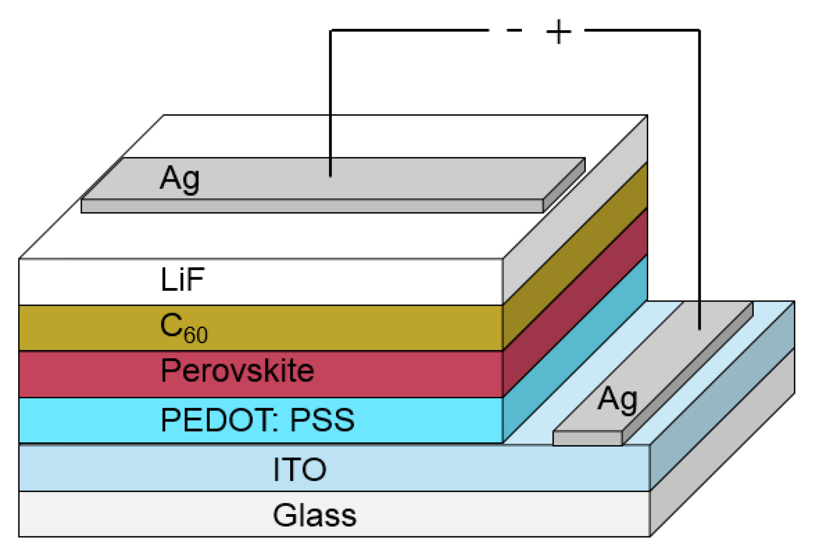
A schematic of the device structure used for optimizing the solar cell performance is shown in Figure 1. We have prepared our devices on glass substrates with a commercial indium-tin-oxide (ITO) layer. As the first layer, we spin-coat PEDOT:PSS, which is used as a base for the perovskite layer that is spin-coated afterwards. The following layers, such as C60, LiF and Ag top contact are consecutively evaporated. Our measurements show that the preparation of the perovskite layer and the evaporation of the C60 layer play significant roles for the final device performance. Therefore, we will focus here in more detail on these layers. All the other layers are processed in a common way and details are described in Section 4.
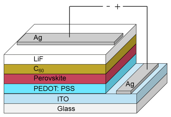
Figure 1.
In this figure, a schematic of the used device structure containing all layers is presented. The layer thicknesses are not in scale. The different layer thicknesses are presented in Section 4.2 for optimized solar cell performance.
2.1. Perovskite Layer
The preparation of perovskite film plays a key role in the fabrication of the whole device. It has been widely accepted that the perovskite crystalization process needs to be carefully tuned to get compact films [39,40]. Perovskite has strong polarity and is prone to forming uncontinuous films. Different precursor solutions and additives have been reported to achieve better film morphology by speeding up [41] or slowing down [38,42,43] the crystallization dynamics. Here, we fabricate a compact and pin-hole free perovskite layer by accelerating the crystallization process by the vacuum assisted one-step solution method (VAOS).
The VAOS method diagram is shown in Figure 2. Simply, mixed halide perovskite solution is spin-coated on ITO/PEDOT:PSS substrates in the glovebox with less than 5 ppm moisture level. Then, the substrates are transferred immediately onto a hotplate in a vacuum chamber. A combination of higher temperature and a vacuum removes very quickly all residual solvent leading to a fast crystallization process in the film, which is expected to be faster than the commonly used temperature annealing without additional vacuum. In Figure 3, the top-view and cross-section SEM image of perovskite films are presented.

Figure 2.
Schematic of the vacuum assisted one-step solution (VAOS) preparation method of the perovskite film.
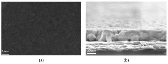
Figure 3.
Smooth, uniform, pin-hole free perovskite film (a) top-view; (b) cross-section SEM images.
The film is quite compact and no pin-holes were observed on the top-view image. On the cross-section image, the perovskite layer on ITO/PEDOT:PSS has a uniform thickness of 300 nm as demonstrated in Figure 3b).
Compared to other methods, because of the fast crystallization process, the perovskite crystals are relatively small and have a wide range of size distribution (from around 100 nm to 1 µm). On the other hand, the crystallization nuclei are forced to pack closely and form a very flat and continuous, virtually pin-hole free film. It is worth mentioning that the film is so flat that no obvious undulation could be observed even for an only 70 nm thick perovskite thin film (see Supplementary Material Figure S1), which enables simple formation of semi-transparent perovskite solar cells by reducing the film thickness. During vacuum annealing, the perovskite film color changed from colorless to red-brown, and longer vacuum annealing leads to a notably darker color. It has been found the vacuum annealing needs to be carefully optimized regarding annealing time and temperature, as soon as fully conversion is completed, further annealing could be harmful leading to perovskite decomposition [44,45]. In our experiments, a vacuum annealing directly after spin-coating of the perovskite film for 4 min at 80 °C leads to the most efficient device performance.
2.2. C60 Layer
2.2.1. Influence of C60 Layer Thickness
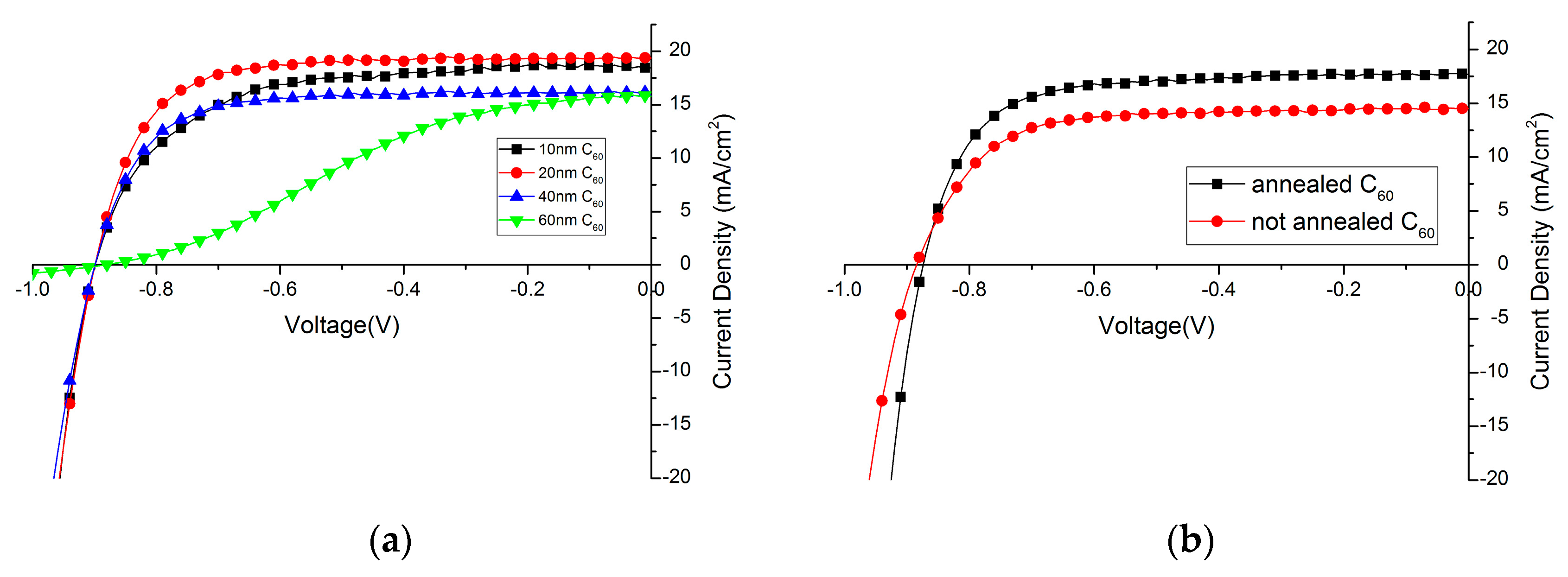
C60 layer is used to act as a selective electron extraction layer in the solar cell. Its thickness needs to be carefully controlled, as it needs to be thick enough to form a compact layer over the perovskite film, but a too thick C60 layer will increase the series resistance of the device. C60 layers with different thickness have been thermally evaporated on top of the perovskite film. In Figure 4a, the influence of the C60 layer thickness on the device performance is shown. Detailed solar cell parameters are summarized in Table 1. Clearly, 20 nm C60 is already enough as a hole-blocking layer, and doubling its thickness greatly impedes its ability to transfer electrons which can be observed in a low fill factor and also lower photocurrent density. If the layer is too thin, the fill factor and photocurrent density also decreases slightly, which is assumed to be due to a not full coverage of the perovskite film without any pinholes. Compared to PCBM, which is usually around 100 nm [30], C60 is more electron-conductive [46] and requires a very flat perovskite film as a layer underneath. Only, in this case, it is possible to have thin, but compact and pinhole-free films.
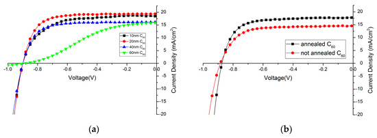
Figure 4.
Influence of C60 layer (a) thickness; and (b) annealing effect on device performance.

Table 1.
Effect of C60 layer thickness on device performance.
2.2.2. Influence of C60 Annealing
It is found that the performance of solar cells will benefit from a short annealing treatment after deposition of C60 layer (10 min at 90 °C in N2 atmosphere), mainly due to the increase of photocurrent. (Figure 4b, Table 2). It has been reported that PCBM strongly diffuses through films when annealed. It is expected that also the C60 diffuses with annealing and changes the perovskite/C60 interface promoting charge transfer [30]. Additional aggregation might increase the charge carrier mobility of the C60 film, thus improving charge collection at the electrode.

Table 2.
Annealing effect of C60 layer.
2.3. Further Optimization
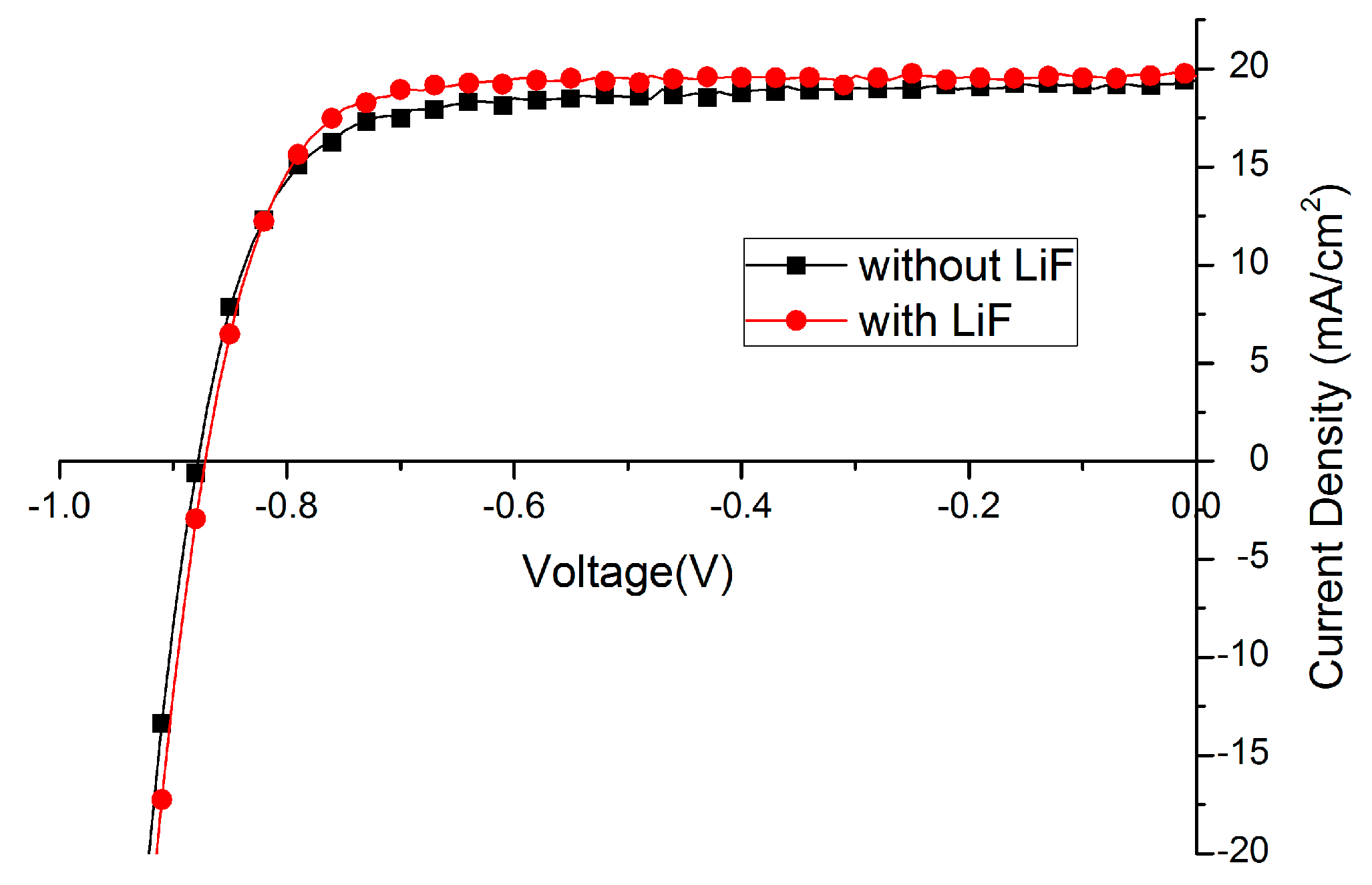
Lithium fluoride (LiF), bathocuproine (BCP) or Ca are widely used as the interfacial layer between electron transport layer (ETL) and metal back contact. In this paper, the effect of LiF is studied. Amazingly, the fill factor (FF) of solar cells could be improved from 70%–75% to around 80% just by depositing 1 nm LiF before Ag evaporation (Figure 5, Table 3). Such an effect has been reported [34,47,48], implying the energy mismatch between cathode and electron transporting layer is compensated by the formation of dipoles with LiF insertion layer. We also expect that the LiF layer protects the layers underneath when the silver is evaporated on top. Less silver will diffuse into the film forming high conducting channels leading to a recombination reducing fill-factor.

Figure 5.
Effect of lithium fluoride (LiF) layer on Current density -Voltage (J–V) curve.

Table 3.
Effect of lithium fluoride (LiF) layer on solar cell performance.
2.4. Optimized Solar Cell Performance and Statistical Results
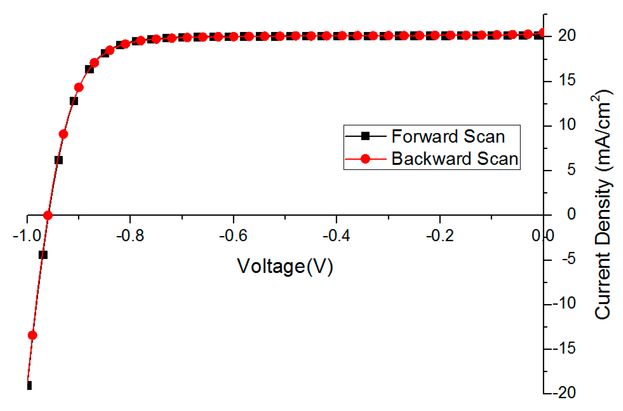
Based on the optimization results mentioned above, we deposited 30 perovskite films and fabricated solar cells in successive three batches. The performance of the best fully optimized solar cell is presented in Figure 6 and Table 4 with no obvious hysteresis behavior.
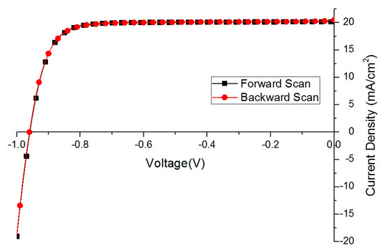
Figure 6.
The best solar cell performance without hysteresis behavior (scan rate 0.1 V/s).

Table 4.
The best perovskite solar cell performance after full optimization.
The FF of the backward scan is lower (79.4 vs. 81.0 in Table 4) mainly due to a steeper current drop at 0 bias points, which is attributed to certain charge accumulation.
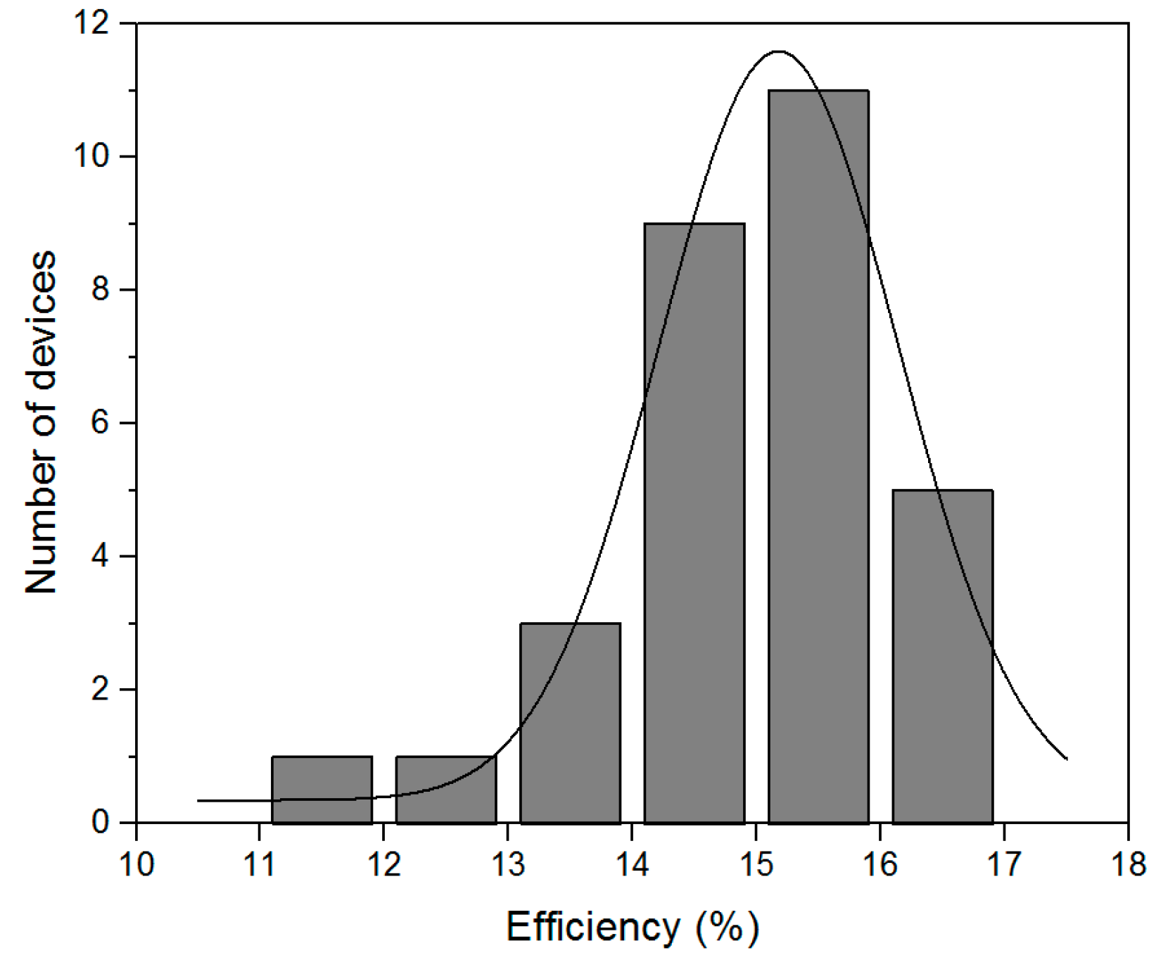
The statistical distribution of these results is shown in Figure 7. As can be seen, our fabrication method is quite reproducible, and over 80% solar cells have over 14% efficiency. The inefficient results are considered to come from intrinsic flaw-prone spin-coating process which, with the oversaturated precursor solution, sometimes induces macroscopic pinholes.
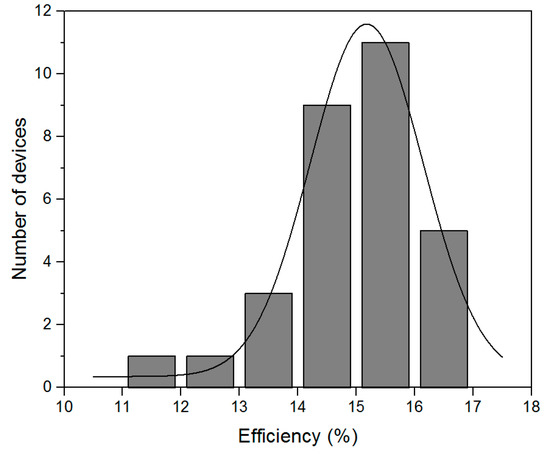
Figure 7.
The statistical distribution of 30 solar cell efficiencies fabricated in three successive processes.
3. Discussion
The optimization results in the previous sections clearly indicate that not only does the perovskite layer preparation play a significant role in the final device performance, but also the interfacial layers. With the described method, we could achieve a champion device efficiency over 16%. Most cells showed a performance exceeding 14% efficiency.
It has been considered that large perovskite crystals are superior to small ones in solar cells, as they have less grain boundaries, thus less recombination and longer charge carrier life time. However, in our case, we show that, even with small perovskite crystals, solar cells still work very efficiently with an over 80% fill factor with optimized C60 and LiF layer. The presented novel VAOS deposition method could produce ultra-thin, ultra-flat and compact perovskite film, and we believe it will contribute to this flourishing research area.
4. Materials and Methods
4.1. Preparation of the Precursor
Methylammonium iodide (MAI) was synthesized as reported [49]. In short, 24 mL of methylamine solution (33% in ethanol, Sigma-Aldrich, Schnelldorf, Germany) was diluted with 100 mL of absolute ethanol in a 250 mL round-bottom flask. In addition, 10 mL of hydroiodic acid (33 wt%) was added under constant stirring into the flask. After reacting one hour at room temperature, the solvents were removed by rotary evaporation. The obtained white solid was washed with dry diethyl ether and finally recrystallized with ethanol. To prepare mixed-halide perovskite precursor solutions, PbI2, PbCl2 and MAI were mixed in anhydrous dimethylformamide (DMF) (99.9%) with a molar ration of 1:1:4 [50]. The solution concentration is around 40 wt%. The solutions were stirred at room temperature overnight in a glovebox and stored there for use.
4.2. Fabrication of the Devices
The ITO-coated glass substrates (15 Ω per sq) were ultrasonic cleaned for 5 min by detergent, acetone and isopropanol successively. Then, they were treated with oxygen plasma for 7 min. After that, around 30 nm PEDOT:PSS (Clevios™ VP AI 4083) film was spin-coated on top (Supplementary Material Figure S2) and then annealed at 180 °C for 5 min. Then, the substrates were transferred to a glovebox with moisture and oxygen level both lower than 5 ppm. The prepared precursor solution was spin-coated on the substrates with 3000 rpm for 20 s. Then, the films were transferred immediately to a vacuum chamber on a hotplate at 90 °C. After evacuating, the films turned red-brown and then were further annealed at normal pressure at 100 °C for full conversion to perovskite. Finally, a C60 layer, LiF layer and Ag back contact were thermally evaporated consecutively on top of the spin-coated perovskite film. Layer thickness details are summarized in Table 5.

Table 5.
Layer deposition technique and thickness of different layers in the optimized solar cell geometry.
4.3. Device Characterization
The morphology of the perovskite film were characterized using a scanning electron microscopy (SEM) (Zeiss Neon 40 EsB, Oberkochen, Germany) operated at 5 kV accelerating voltage. Current density-voltage (J–V) measurements were performed using a Keithley 2400 SourceMeter (Tektronix GmbH, Keithley Instruments, Germering, Germany) controlled through a self-written LabView program (National Instruments, Austin, Texas, US). Cells were illuminated via a LOT-Oriel LS0106 solar simulator (LOT, Darmstadt, Germany) through a shadow mask with a resulting active area of 0.09 cm2. Light intensities were calibrated with a certified Si reference solar cell (Fraunhofer Institute, Freiburg, Germany) with a KG5 filter (Schott, Mainz, Germany). The light intensity of the solar simulator was around 0.95 sun.
Supplementary Materials
The following are available online at: http://www.mdpi.com/1420-3049/21/4/542/s1, Figure S1: Ultraflat perovskite film with around 70 nm thickness deposited with the VAOS method, Figure S2: Cross-section SEM graph of PEDOT:PSS film.
Acknowledgments
We acknowledge funding The Federal Ministry of Education and Research (BMBF) (MesoPIN project) and the Baden–Württemberg Foundation (BioMats-SuperSol project). H.H. thanks the Chinese Scholarship Council (CSC) and K.K.W. the German Academic Exchange Service (DAAD) for funding.
Author Contributions
H.H. and K.K.W. conceived and designed the experiments. Experiments were conducted by H.H. T.K., F.H., S.P. and P.D. contributed to precursor synthesis and perovskite film preparation. L.S.-M. supervised the project. H.H. and L.S.-M. wrote the manuscript. All authors contributed to the discussion of the results.
Conflicts of Interest
The authors declare no conflict of interest.
References
- Kojima, A.; Teshima, K.; Shirai, Y.; Miyasaka, T. Organometal Halide Perovskites as Visible-Light Sensitizers for Photovoltaic Cells. J. Am. Chem. Soc. 2009, 131, 6050–6051. [Google Scholar] [CrossRef] [PubMed]
- Yang, W.S.; Noh, J.H.; Jeon, N.J.; Kim, Y.C.; Ryu, S.; Seo, J.; Seok, S.I. High-performance photovoltaic perovskite layers fabricated through intramolecular exchange. Science 2015, 348, 1234–1237. [Google Scholar] [CrossRef] [PubMed]
- Jeon, N.J.; Noh, J.H.; Yang, W.S.; Kim, Y.C.; Ryu, S.; Seo, J.; Seok, S.I. Compositional engineering of perovskite materials for high-performance solar cells. Nature 2015, 517, 476–480. [Google Scholar] [CrossRef] [PubMed]
- Walsh, A. Principles of Chemical Bonding and Band Gap Engineering in Hybrid Organic-Inorganic Halide Perovskites. J. Phys. Chem. C 2015, 119, 5755–5760. [Google Scholar] [CrossRef] [PubMed]
- Noh, J.H.; Im, S.H.; Heo, J.H.; Mandal, T.N.; Seok, S.I. Chemical Management for Colorful, Efficient, and Stable Inorganic-Organic Hybrid Nanostructured Solar Cells. Nano Lett. 2013, 13, 1764–1769. [Google Scholar] [CrossRef] [PubMed]
- Kulkarni, S.A.; Baikie, T.; Boix, P.P.; Yantara, N.; Mathews, N.; Mhaisalkar, S. Band-gap tuning of lead halide perovskites using a sequential deposition process. J. Mater. Chem. A 2014, 2, 9221–9225. [Google Scholar] [CrossRef]
- D’Innocenzo, V.; Srimath Kandada, A.R.; De Bastiani, M.; Gandini, M.; Petrozza, A. Tuning the Light Emission Properties by Band Gap Engineering in Hybrid Lead Halide Perovskite. J. Am. Chem. Soc. 2014, 136, 17730–17733. [Google Scholar] [CrossRef] [PubMed]
- De Wolf, S.; Holovsky, J.; Moon, S.-J.; Löper, P.; Niesen, B.; Ledinsky, M.; Haug, F.-J.; Yum, J.-H.; Ballif, C. Organometallic Halide Perovskites: Sharp Optical Absorption Edge and its Relation to Photovoltaic Performance. J. Phys. Chem. Lett. 2014, 5, 1035–1039. [Google Scholar] [CrossRef] [PubMed]
- Zhu, X.; Su, H.; Marcus, R.A.; Michel-Beyerle, M.E. Computed and Experimental Absorption Spectra of the Perovskite CH3NH3PbI3. J. Phys. Chem. Lett. 2014, 5, 3061–3065. [Google Scholar] [CrossRef] [PubMed]
- Dong, Q.; Fang, Y.; Shao, Y.; Mulligan, P.; Qiu, J.; Cao, L.; Huang, J. Electron-hole diffusion lengths > 175 µm in solution-grown CH3NH3PbI3 single crystals. Science 2015, 347, 967–970. [Google Scholar] [CrossRef] [PubMed]
- Shi, D.; Adinolfi, V.; Comin, R.; Yuan, M.; Alarousu, E.; Buin, A.; Chen, Y.; Hoogland, S.; Rothenberger, A.; Katsiev, K.; et al. Low trap-state density and long carrier diffusion in organolead trihalide perovskite single crystals. Science 2015, 347, 519–522. [Google Scholar] [CrossRef] [PubMed]
- Stranks, S.D.; Eperon, G.E.; Grancini, G.; Menelaou, C.; Alcocer, M.J.P.; Leijtens, T.; Herz, L.M.; Petrozza, A.; Snaith, H.J. Electron-Hole Diffusion Lengths Exceeding 1 Micrometer in an Organometal Trihalide Perovskite Absorber. Science 2013, 342, 341–344. [Google Scholar] [CrossRef] [PubMed]
- Xing, G.; Mathews, N.; Sun, S.; Lim, S.S.; Lam, Y.M.; Gratzel, M.; Mhaisalkar, S.; Sum, T.C. Long-Range Balanced Electron- and Hole-Transport Lengths in Organic-Inorganic CH3NH3PbI3. Science 2013, 342, 344–347. [Google Scholar] [CrossRef] [PubMed]
- Im, J.H.; Lee, C.R.; Lee, J.W.; Park, S.W.; Park, N.G. 6.5% efficient perovskite quantum-dot-sensitized solar cell. Nanoscale 2011, 3, 4088–4093. [Google Scholar] [CrossRef] [PubMed]
- Etgar, L.; Gao, P.; Xue, Z.S.; Peng, Q.; Chandiran, A.K.; Liu, B.; Nazeeruddin, M.K.; Gratzel, M. Mesoscopic CH3NH3PbI3/TiO2 Heterojunction Solar Cells. J. Am. Chem. Soc. 2012, 134, 17396–17399. [Google Scholar] [CrossRef] [PubMed]
- Kim, H.S.; Lee, C.R.; Im, J.H.; Lee, K.B.; Moehl, T.; Marchioro, A.; Moon, S.J.; Humphry-Baker, R.; Yum, J.H.; Moser, J.E.; et al. Lead Iodide Perovskite Sensitized All-Solid-State Submicron Thin Film Mesoscopic Solar Cell with Efficiency Exceeding 9%. Sci. Rep. 2012, 2, 591. [Google Scholar] [CrossRef] [PubMed]
- Zhou, H.; Chen, Q.; Li, G.; Luo, S.; Song, T.-B.; Duan, H.-S.; Hong, Z.; You, J.; Liu, Y.; Yang, Y. Interface engineering of highly efficient perovskite solar cells. Science 2014, 345, 542–546. [Google Scholar] [CrossRef] [PubMed]
- Chen, Q.; Zhou, H.; Hong, Z.; Luo, S.; Duan, H.-S.; Wang, H.-H.; Liu, Y.; Li, G.; Yang, Y. Planar heterojunction perovskite solar cells via vapor assisted solution process. J. Am. Chem. Soc. 2013, 136, 622–625. [Google Scholar] [CrossRef] [PubMed]
- Liu, M.; Johnston, M.B.; Snaith, H.J. Efficient planar heterojunction perovskite solar cells by vapour deposition. Nature 2013, 501, 395–398. [Google Scholar] [CrossRef] [PubMed]
- Kim, H.-S.; Park, N.-G. Parameters Affecting I–V Hysteresis of CH3NH3PbI3 Perovskite Solar Cells: Effects of Perovskite Crystal Size and Mesoporous TiO2 Layer. J. Phys. Chem. Lett. 2014, 5, 2927–2934. [Google Scholar] [CrossRef] [PubMed]
- Shao, Y.H.; Xiao, Z.G.; Bi, C.; Yuan, Y.B.; Huang, J.S. Origin and elimination of photocurrent hysteresis by fullerene passivation in CH3NH3PbI3 planar heterojunction solar cells. Nat. Commun. 2014, 5, 5784. [Google Scholar] [CrossRef] [PubMed]
- Heo, J.H.; You, M.S.; Chang, M.H.; Yin, W.; Ahn, T.K.; Lee, S.-J.; Sung, S.-J.; Kim, D.H.; Im, S.H. Hysteresis-less mesoscopic CH3NH3PbI3 perovskite hybrid solar cells by introduction of Li-treated TiO2 electrode. Nano Energy 2015, 15, 530–539. [Google Scholar] [CrossRef]
- Jena, A.K.; Chen, H.-W.; Kogo, A.; Sanehira, Y.; Ikegami, M.; Miyasaka, T. The Interface between FTO and the TiO2 Compact Layer Can Be One of the Origins to Hysteresis in Planar Heterojunction Perovskite Solar Cells. ACS Appl. Mater. Interfaces 2015, 7, 9817–9823. [Google Scholar] [CrossRef] [PubMed]
- Docampo, P.; Ball, J.M.; Darwich, M.; Eperon, G.E.; Snaith, H.J. Efficient organometal trihalide perovskite planar-heterojunction solar cells on flexible polymer substrates. Nat. Commun. 2013, 4, 2761. [Google Scholar] [CrossRef] [PubMed]
- Forgacs, D.; Sessolo, M.; Bolink, H.J. Lead acetate precursor based p-i-n perovskite solar cells with enhanced reproducibility and low hysteresis. J. Mater. Chem. A 2015, 3, 14121–14125. [Google Scholar] [CrossRef]
- Heo, J.H.; Han, H.J.; Kim, D.; Ahn, T.K.; Im, S.H. Hysteresis-less inverted CH3NH3PbI3 planar perovskite hybrid solar cells with 18.1% power conversion efficiency. Energy Environ. Sci. 2015, 8, 1602–1608. [Google Scholar] [CrossRef]
- Wu, C.-G.; Chiang, C.-H.; Tseng, Z.-L.; Nazeeruddin, M.K.; Hagfeldt, A.; Gratzel, M. High efficiency stable inverted perovskite solar cells without current hysteresis. Energy Environ. Sci. 2015, 8, 2725–2733. [Google Scholar] [CrossRef]
- Heo, J.H.; Im, S.H. Highly reproducible, efficient hysteresis-less CH3NH3PbI3-xClx planar hybrid solar cells without requiring heat-treatment. Nanoscale 2016, 8, 2554–2560. [Google Scholar] [CrossRef] [PubMed]
- El-Henawey, M.I.; Gebhardt, R.S.; El-Tonsy, M.M.; Chaudhary, S. Organic solvent vapor treatment of lead iodide layers in the two-step sequential deposition of CH3NH3PbI3-based perovskite solar cells. J. Mater. Chem. A 2016, 4, 1947–1952. [Google Scholar] [CrossRef]
- Chiang, C.-H.; Tseng, Z.-L.; Wu, C.-G. Planar heterojunction perovskite/PC71BM solar cells with enhanced open-circuit voltage via a (2/1)-step spin-coating process. J. Mater. Chem. A 2014, 2, 15897–15903. [Google Scholar] [CrossRef]
- Chiang, Y.-F.; Jeng, J.-Y.; Lee, M.-H.; Peng, S.-R.; Chen, P.; Guo, T.-F.; Wen, T.-C.; Hsu, Y.-J.; Hsu, C.-M. High voltage and efficient bilayer heterojunction solar cells based on an organic-inorganic hybrid perovskite absorber with a low-cost flexible substrate. Phys. Chem. Chem. Phys. 2014, 16, 6033–6040. [Google Scholar] [CrossRef] [PubMed]
- Jeng, J.Y.; Chen, K.C.; Chiang, T.Y.; Lin, P.Y.; Tsai, T.D.; Chang, Y.C.; Guo, T.F.; Chen, P.; Wen, T.C.; Hsu, Y.J. Nickel oxide electrode interlayer in CH3NH3PbI3 perovskite/PCBM planar-heterojunction hybrid solar cells. Adv. Mater. 2014, 26, 4107–4113. [Google Scholar] [CrossRef] [PubMed]
- Jeng, J.Y.; Chiang, Y.F.; Lee, M.H.; Peng, S.R.; Guo, T.F.; Chen, P.; Wen, T.C. CH3NH3PbI3 Perovskite/Fullerene Planar-Heterojunction Hybrid Solar Cells. Adv. Mater. 2013, 25, 3727–3732. [Google Scholar] [CrossRef] [PubMed]
- Seo, J.; Park, S.; Chan Kim, Y.; Jeon, N.J.; Noh, J.H.; Yoon, S.C.; Seok, S.I. Benefits of very thin PCBM and LiF layers for solution-processed p-i-n perovskite solar cells. Energy Environ. Sci. 2014, 7, 2642–2646. [Google Scholar] [CrossRef]
- Even, J.; Pedesseau, L.; Katan, C.; Kepenekian, M.; Lauret, J.-S.; Sapori, D.; Deleporte, E. A Solid State Physics Perspective on Hybrid Perovskite Semiconductors. J. Phys. Chem. C 2015, 119, 10161–10177. [Google Scholar] [CrossRef]
- Gong, X.; Li, M.; Shi, X.-B.; Ma, H.; Wang, Z.-K.; Liao, L.-S. Controllable Perovskite Crystallization by Water Additive for High-Performance Solar Cells. Adv. Funct. Mater. 2015, 25, 6671–6678. [Google Scholar] [CrossRef]
- Chiang, C.-H.; Wu, C.-G. Bulk heterojunction perovskite–PCBM solar cells with high fill factor. Nat. Photon 2016, 10, 196–200. [Google Scholar] [CrossRef]
- Liang, P.W.; Liao, C.Y.; Chueh, C.C.; Zuo, F.; Williams, S.T.; Xin, X.K.; Lin, J.; Jen, A.K. Additive enhanced crystallization of solution-processed perovskite for highly efficient planar-heterojunction solar cells. Adv. Mater. 2014, 26, 3748–3754. [Google Scholar] [CrossRef] [PubMed]
- Moore, D.T.; Sai, H.; Tan, K.W.; Smilgies, D.M.; Zhang, W.; Snaith, H.J.; Wiesner, U.; Estroff, L.A. Crystallization kinetics of organic-inorganic trihalide perovskites and the role of the lead anion in crystal growth. J. Am. Chem. Soc. 2015, 137, 2350–2358. [Google Scholar] [CrossRef] [PubMed]
- Tidhar, Y.; Edri, E.; Weissman, H.; Zohar, D.; Hodes, G.; Cahen, D.; Rybtchinski, B.; Kirmayer, S. Crystallization of Methyl Ammonium Lead Halide Perovskites: Implications for Photovoltaic Applications. J. Am. Chem. Soc. 2014, 136, 13249–13256. [Google Scholar] [CrossRef] [PubMed]
- Zhang, W.; Saliba, M.; Moore, D.T.; Pathak, S.K.; Horantner, M.T.; Stergiopoulos, T.; Stranks, S.D.; Eperon, G.E.; Alexander-Webber, J.A.; Abate, A.; et al. Ultrasmooth organic-inorganic perovskite thin-film formation and crystallization for efficient planar heterojunction solar cells. Nat. Commun. 2015, 6, 6142. [Google Scholar] [CrossRef] [PubMed]
- Chang, C.-Y.; Chu, C.-Y.; Huang, Y.-C.; Huang, C.-W.; Chang, S.-Y.; Chen, C.-A.; Chao, C.-Y.; Su, W.-F. Tuning Perovskite Morphology by Polymer Additive for High Efficiency Solar Cell. ACS Appl. Mater. Interfaces 2015, 7, 4955–4961. [Google Scholar] [CrossRef] [PubMed]
- Heo, J.H.; Song, D.H.; Im, S.H. Planar CH3NH3PbBr3 hybrid solar cells with 10.4% power conversion efficiency, fabricated by controlled crystallization in the spin-coating process. Adv. Mater. 2014, 26, 8179–8183. [Google Scholar] [CrossRef] [PubMed]
- Schoonman, J. Organic–inorganic lead halide perovskite solar cell materials: A possible stability problem. Chem. Phys. Lett. 2015, 619, 193–195. [Google Scholar] [CrossRef]
- Conings, B.; Drijkoningen, J.; Gauquelin, N.; Babayigit, A.; D’Haen, J.; D’Olieslaeger, L.; Ethirajan, A.; Verbeeck, J.; Manca, J.; Mosconi, E.; et al. Intrinsic Thermal Instability of Methylammonium Lead Trihalide Perovskite. Adv. Energy Mater. 2015, 5, 1500477–1500485. [Google Scholar] [CrossRef]
- Liang, P.W.; Chueh, C.C.; Williams, S.T.; Jen, A.K.Y. Roles of Fullerene-Based Interlayers in Enhancing the Performance of Organometal Perovskite Thin-Film Solar Cells. Adv. Energy Mater. 2015, 5, 1402321–1402327. [Google Scholar] [CrossRef]
- Sun, K.; Chang, J.; Isikgor, F.H.; Li, P.; Ouyang, J. Efficiency enhancement of planar perovskite solar cells by adding zwitterion/LiF double interlayers for electron collection. Nanoscale 2015, 7, 896–900. [Google Scholar] [CrossRef] [PubMed]
- Liu, X.; Yu, H.; Yan, L.; Dong, Q.; Wan, Q.; Zhou, Y.; Song, B.; Li, Y. Triple cathode buffer layers composed of PCBM, C60, and LiF for high-performance planar perovskite solar cells. ACS Appl. Mater. Interfaces 2015, 7, 6230–6237. [Google Scholar] [CrossRef] [PubMed]
- Binek, A.; Hanusch, F.C.; Docampo, P.; Bein, T. Stabilization of the Trigonal High-Temperature Phase of Formamidinium Lead Iodide. J. Phys. Chem. Lett. 2015, 6, 1249–1253. [Google Scholar] [CrossRef] [PubMed]
- Wang, D.; Liu, Z.; Zhou, Z.; Zhu, H.; Zhou, Y.; Huang, C.; Wang, Z.; Xu, H.; Jin, Y.; Fan, B.; et al. Reproducible One-Step Fabrication of Compact MAPbI3-xClxThin Films Derived from Mixed-Lead-Halide Precursors. Chem. Mat. 2014, 26, 7145–7150. [Google Scholar] [CrossRef]
- Sample Availability: Not available.
© 2016 by the authors. Licensee MDPI, Basel, Switzerland. This article is an open access article distributed under the terms and conditions of the Creative Commons by Attribution (CC-BY) license ( http://creativecommons.org/licenses/by/4.0/).

