Article

Origins of Giant Dielectric Properties with Low Loss Tangent in Rutile (Mg1/3Ta2/3)0.01Ti0.99O2 Ceramic

by
Nateeporn Thongyong
1,
Narong Chanlek
2,
Pornjuk Srepusharawoot
1 and
Prasit Thongbai
1,*
1
Giant Dielectric and Computational Design Research Group (GD–CDR), Department of Physics, Faculty of Science, Khon Kaen University, Khon Kaen 40002, Thailand
2
Synchrotron Light Research Institute (Public Organization), 111 University Avenue, Muang District, Nakhon Ratchasima 30000, Thailand
*
Author to whom correspondence should be addressed.
Molecules 2021, 26(22), 6952; https://doi.org/10.3390/molecules26226952
Submission received: 30 September 2021 / Revised: 13 November 2021 / Accepted: 14 November 2021 / Published: 17 November 2021
(This article belongs to the Section Materials Chemistry)

Abstract

:
The Mg2+/Ta5+ codoped rutile TiO2 ceramic with a nominal composition (Mg1/3Ta2/3)0.01Ti0.99O2 was synthesized using a conventional solid-state reaction method and sintered at 1400 °C for 2 h. The pure phase of the rutile TiO2 structure with a highly dense microstructure was obtained. A high dielectric permittivity (2.9 × 10⁴ at 103 Hz) with a low loss tangent (<0.025) was achieved in the as-sintered ceramic. After removing the outer surface, the dielectric permittivity of the polished ceramic increased from 2.9 × 10⁴ to 6.0 × 10⁴, while the loss tangent also increased (~0.11). The dielectric permittivity and loss tangent could be recovered to the initial value of the as-sintered ceramic by annealing the polished ceramic in air. Notably, in the temperature range of −60–200 °C, the dielectric permittivity (103 Hz) of the annealed ceramic was slightly dependent (<±4.4%), while the loss tangent was very low (0.015–0.036). The giant dielectric properties were likely contributed by the insulating grain boundaries and insulative surface layer effects.

1. Introduction

Multilayer ceramic capacitors (MLCCs) are essential components in microelectronics applications throughout the development of technology. With the rapid growth of the electronic industry, the efficiency potential of MLCCs is demanded. The crucial way to significantly improve the properties of MLCCS is to use a giant dielectric material with a high dielectric permittivity of ε′ > 104. Numerous types of giant dielectric material have been developed in past decades, such as CaCu3Ti4O12 (CCTO) and related ACu3Ti4O12 compounds [1,2,3,4,5,6], CuO [7], AFe1/2B1/2O3 (A = Ba, Sr, Ca; B = Nb, Ta, Sb) [8], (Li, Ti) doped NiO [9], and codoped SrTiO3-based ceramics [10]. However, the dielectric loss tangent (tanδ) of most giant dielectric oxides is still huge (>>0.1), which is not required for use in MLCCs. Thus, the importance of developing MLCCs with good temperature stability and electroceramics for high energy density capacitors has been widely reported [11,12,13].
In 2013, the first experiment on TiO2 codoped with acceptors/donors was reported [14]. The (ln1/2Nb1/2)0.1Ti0.90O2 exhibited outstanding dielectric performance properties, including a high ε′ (>104), low tanδ (<0.02), and slight temperature dependence of ε′ over a wide range. A new approach to this research is the electron-pinned defect dipole (EPDDs) mechanism, which was proposed as the source of the excellent dielectric behavior. Free electrons in the rutile TiO2 structure, which can be produced by doping with Nb5+, are localized in the 2 l n 3 + + V o + 2 T i 3 + + 2 N b 5 + + T i 4 + defect clusters under an applied electric field. Codoping an electron donor into the rutile TiO2 structure can produce a high ε′ with a low tanδ. The substitution of TiO2 with electron acceptor dopants was necessary to reduce tanδ by restricting the long range movement within defect clusters.
The enhancement of the giant dielectric properties of TiO2 by codoping it with acceptor–donor dopants has been intensively studied, including Ga3+/Nb5+ [15], Ga3+/Ta5+ [16], Al3+/Nb5+ [17], Al3+/Ta5+ [18], Zn2+/Nb5+ [19,20], and Ag+/Nb5+ (or Ta5+/W6+) [21,22,23]. Wei et al. [24] reported significantly enhanced dielectric properties with ε′ ≈ 3.0 × 10⁴ and low tanδ ≈ 0.05. Dong et al. [24] reported a significant improvement of the dielectric properties of Mg2+/Ta5+ codoped TiO2 ceramics, which were described by the formation of the EPDDs. According to the previous works, the internal barrier layer capacitor (IBLC) [25,26,27], surface barrier layer capacitor (SBLC) [15,28,29], and small polaron hopping models [30,31] were also proposed to be the primary origins of the giant dielectric properties of the Ga3+/Ta5+, Al3+/Ta5+, and In3+/Nb5+ codoped TiO2 ceramics. Furthermore, broad-band dielectric spectroscopy up to the THz IR range showed that the giant dielectric response in codoped TiO2 ceramics was clearly attributed to the IBLC effect [32,33]. Therefore, it is important to systematically study the possible origins of the giant dielectric responses in TiO2 ceramics codoped with +2/+5 dopants, which had never before been reported. Thus, the objective of this work was to systematically study the effects of EPDD, IBLC, and SBLC on the giant dielectric properties of Mg2+/Ta5+ codoped TiO2 ceramic to seek the primary origin of the giant dielectric response in that ceramic.
In this work, the Mg2+/Ta5+ codoped TiO2 ceramic was prepared using a solid-state reaction (SSR) method. The phase structure and microstructure of the Mg2+/Ta5+ codoped TiO2 ceramic were characterized. The dielectric properties of as-sintered and polished Mg2+/Ta5+ codoped TiO2 ceramics were investigated. A high ε′ with a low tanδ was achieved in the as-sintered Mg2+/Ta5+ codoped TiO2 ceramic. After removing the outer surface layers, the dielectric properties changed significantly. The dielectric properties of the polished ceramic could be recovered to the initial value by the annealing process. It was found that the temperature stability of the ε′ could be tuned by suppressing the SBLC effect. Furthermore, a broadband dielectric spectroscopy was performed to explain all possible origins of the giant dielectric phenomena in the Mg2+/Ta5+ codoped TiO2 ceramics.

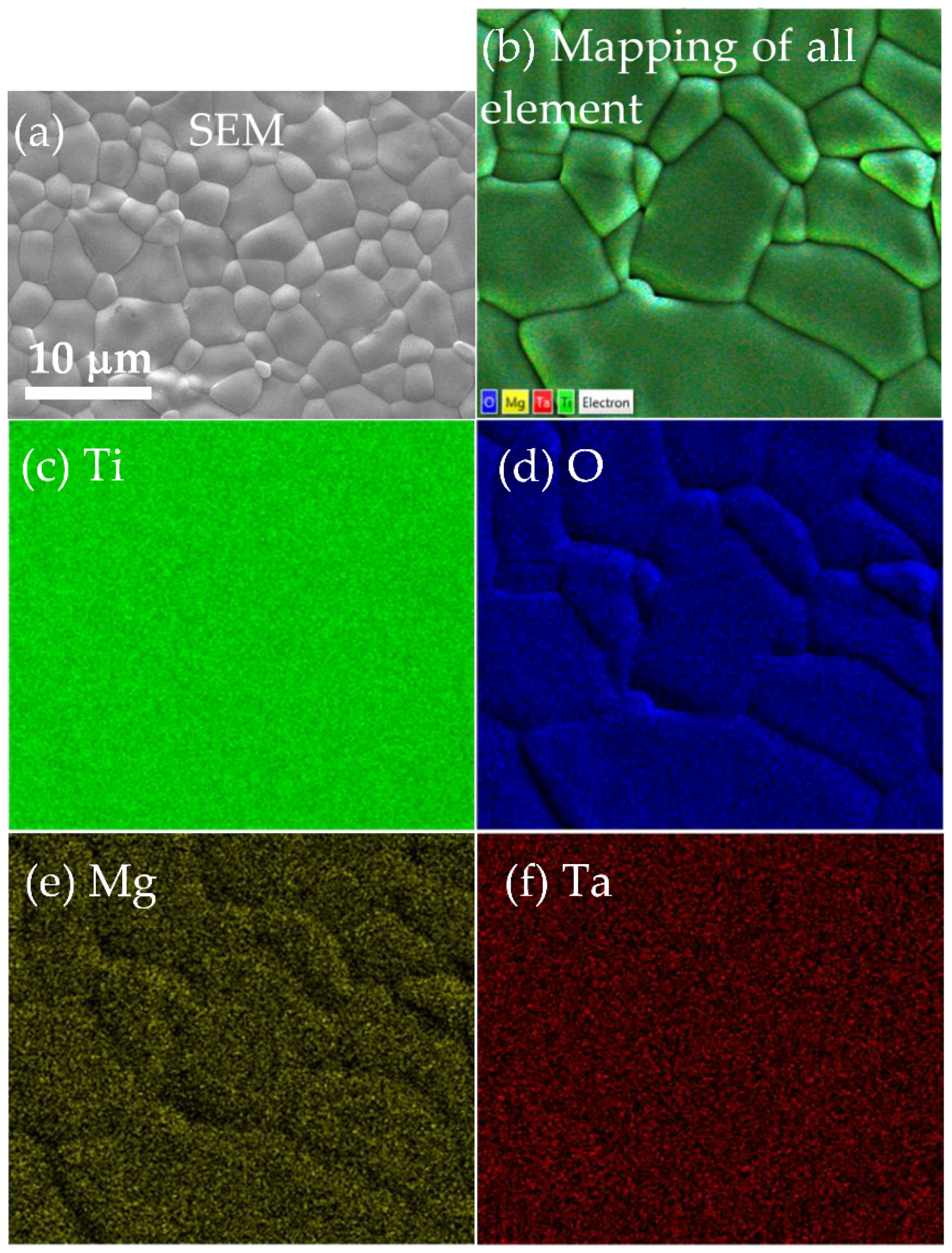
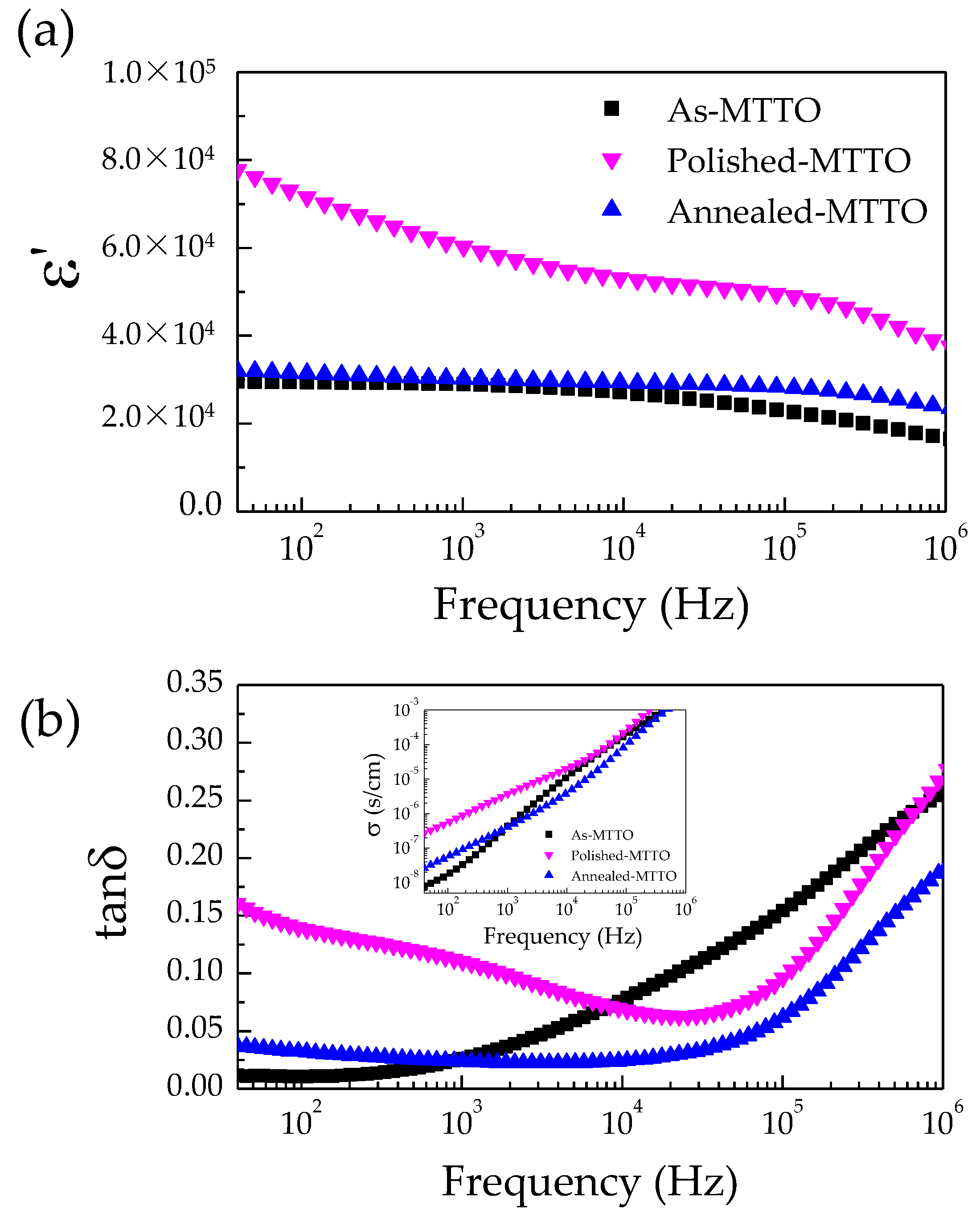
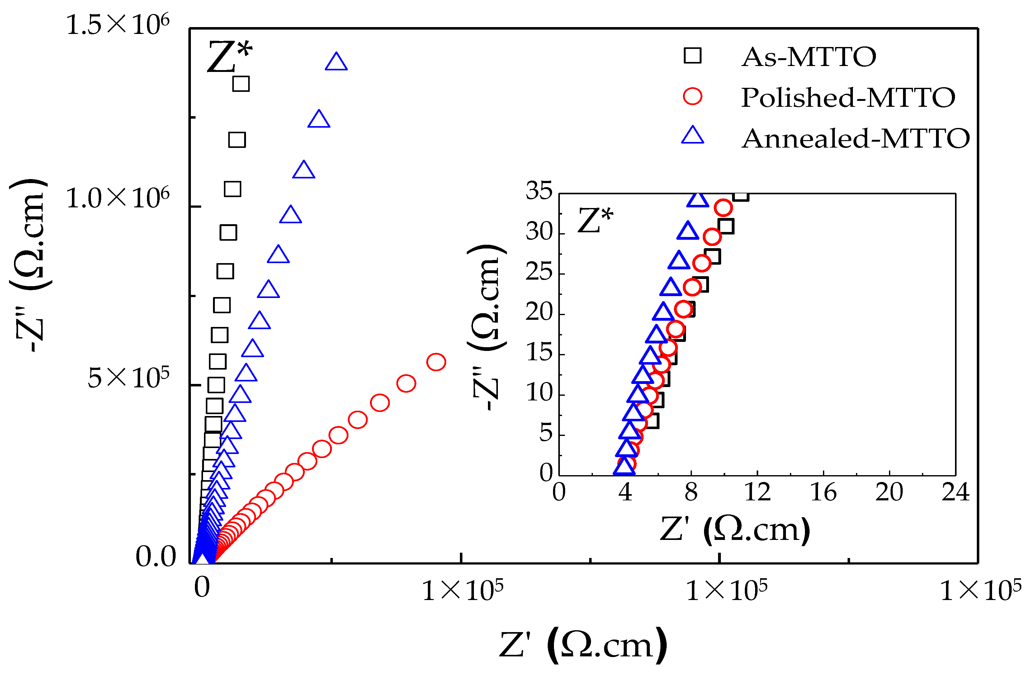
2. Results and Discussion

The XRD patterns of the as-MTTO, polished MTTO, and annealed MTTO ceramics are shown in Figure 1a. A single phase of rutile TiO2 was obtained in all ceramic samples (JCPDS #21-1276). No impurity was detected, indicating the substitution of TiO2 by Mg2+ and Ta5+ due to the small mismatch of the ionic radii between Ta5+ (r6 = 64 pm), Mg2+ (r6 = 72 pm), and Ti4+ (r6 = 60.5 pm). This result was similar to other acceptors/donors codoped TiO2 systems reported in the literature [18,21,24]. There was no segregation of any additional phase on the outer surface and in the inner core of the ceramic samples. Furthermore, the annealing process (800 °C for 30 min) did not result in the segregation of a new phase. Thus, it was expected that only defects on the outer surface would change. The lattice parameters (a and c values) of all the ceramics are shown in Table 1. The a or c value for all the ceramic samples was nearly the same owing to the same codoping concentration. Nevertheless, the a and c values of all the ceramic samples were still larger than those pf the undoped rutile TiO2, confirming that the Mg2+ and Ta5+ can completely replace Ti4+ ions in the crystal lattice [34].
Due to the crystallite size, modification of the cell parameters can also affect the Raman intensity and peak position. Thus, the Raman spectra spectroscopy of the pure TiO2, as-MTTO, polished MTTO, and annealed MTTO were needed, displayed in Figure 1b. The pure TiO2 showed the highest intensity of Raman peak, indicating its highest crystallinity [35]. The Raman peak intensity of TiO2 decreased with codoping with Mg2+/Ta5+. The codoping enhanced the distortion of the host lattice, reducing its crystallinity. For this reason, the annealing process was modifying the defect equilibrium that may reduce the crystallinity on the surface. The Raman active modes (i.e., B1g, Eg, and A1g) were observed. The A1g peak corresponded to the symmetric stretching of the O–Ti–O bonds in [110] plane, while the Eg peak was due to oxygen atom liberation along with the c-axis being out of phase [17,36,37,38]. The peak positions of the Eg and A1g modes are summarized in Table 1. It is worth noting that the peak positions of the Eg and A1g modes for the as-MTTO, polished MTTO, and annealed MTTO ceramics did not change due to the same codoping concentration. Generally, the existence of oxygen vacancies in MTTO ceramics has been attributed to the Mg2+ doping ions according to the following Equation [17]:
M g O T i O 2 M g i T i + V o + O o
The concentrations of defects, especially for oxygen vacancies, on the surfaces of the as-MTTO, polished MTTO, and annealed MTTO ceramic samples were slightly different. However, the slight differences in defects may have had a pronounced effect on the dielectric properties of the MTTO ceramics samples.
Figure 2a shows the dense microstructure of the as-MTTO ceramic sample, with an average grain size of around 3.9 ± 1.3 µm. Furthermore, the SEM mapping image of all elements in the as-MTTO ceramic sample is shown in Figure 2b. The element mapping images of the Ti, O, Mg, and Ta are shown in Figure 2c–f, respectively. There was no segregation of any elements in a specific region.
The dielectric properties as a function of the frequencies of the as-MTTO, polished MTTO, and annealed MTTO ceramics were studied. Usually, the ε′ value of the undoped TiO2 ceramic is about 250 due to a lattice vibration or ionic polarization [39]. The ε′ value of the Ta5+ (or Nb5+) single doped TiO2 ceramic be extremely increased to 104–105 in the radio frequency range, while the tanδ value can also be significantly increased [14,16,40]. The simultaneously increased ε′ and tanδ values can be explained by electron hopping [14,15,16,24,41]. The substitution of rutile TiO2 with Ta5+ can produce free electrons, according to the following Equations:
  2 T i O 2 + T a 2 O 5 4 T i O 2 2 T a T i + 2 T i T i + 8 O 0 + 0.5 O 2
T i 4 + + e T i 3 +
Nevertheless, the substitution of Ta5+ (or Nb5+) doped TiO2 with acceptor dopants (e.g., Ag+, Zn2+, or In3+) can cause a significant decrease in the tanδ value [14,16,20,23,40]. The reduced tanδ value has been explained by many factors such as defect clusters [14], insulating grain boundaries [20,42], and insulative outer surface layers [16,28,29,43]. It was reported that a high ε′ and low tanδ can be obtained in as-sintered In3+/Nb5+ codoped TiO2 ceramics or annealed In3+/Nb5+ codoped TiO2 ceramics [28,29,42]. The tanδ value can be significantly increased after removing the outer surface layer [28,42]. As illustrated in Figure 3a,b, a high ε′ (>104) over the measured frequency range can be obtained in the as-MTTO ceramic, while a low tanδ (<0.05) was achieved in the frequency range below 2 kHz. After removing the outer surface layer, the ε′ of the polished MTTO ceramic was increased by a factor of two compared to that of the as-MTTO ceramic. However, the tanδ value of the polished MTTO ceramic was also increased by more than two times over the measured frequency range. Surprisingly, the ε′ value of the annealed MTTO ceramic could be returned to the initial value of the as-MTTO ceramic by annealing in air. Furthermore, a low tanδ (<0.05) could be extended to a higher frequency range of 105 Hz compared to that of the as-MTTO ceramic. This observation indicates that the outer surface layer had a remarkable influence on the overall dielectric properties of the MTTO ceramics, which was similar to that observed in other codoped TiO2 systems such as Ga3+/Ta5+ [16], In3+/Nb5+ [28], and Al3+/Nb5+ [17]. The ε′ values at 1 kHz of the as-MTTO, polished MTTO, and annealed MTTO ceramics were 28,970, 60,221, and 30,249, respectively, while the tanδ values at 1 kHz were 0.026, 0.110, and 0.024, respectively. The dielectric properties of the polished MTTO ceramic are comparable those +2/+5 codoped TiO2 systems, as summarized in Table 2.
After removing the outer surface layer, the tanδ and associated low frequency conductivity of the polished MTTO ceramic (inset of Figure 3b) increased significantly, indicating the insulating nature of the outer surface layer. After removing the insulating surface layer, the outer surface of the polished MTTO ceramic became a semiconductor. Generally, the Schottky barrier height (SBH) can be created at the interface between the electrode and semiconducting core in accordance with the Schottky–Mott theory [44]. The SBH is dependent on the different work functions between the electron affinity of the semiconductor and that of the metal electrode. Therefore, the highest ε′ value of the polished MTTO ceramic has been attributed to the artificial interfacial polarization at the sample–electrode interface, which is associated with DC conduction. However, this is usually accompanied by an increase in tanδ. Note that the SBH could not be created on the surface of the as-MTTO ceramic due to its insulating outer surface skin. The dielectric properties of the annealed MTTO ceramic were almost entirely returned to the initial properties of the as-MTTO ceramic. These results indicate that the formation of the SBH was inhibited in the annealed MTTO ceramic due to its insulating outer surface layer, just like the as-MTTO ceramic. Typically, the annealing process can fill oxygen vacancies on the surfaces and/or along the grain boundaries, converting the semiconducting surface to an insulating surface, according to Equation (4) [45].
1 2 O 2 + V o + 2 e O O x
Notably, it was also observed that the dielectric properties of the annealed MTTO ceramic were better than those of the as-MTTO ceramic. The ε′ of the annealed MTTO ceramic was more stable in frequency than that of the as-MTTO ceramic, while a low tanδ (<0.05) value was extended to a higher frequency range. The temperature dependence of the dielectric properties of the as-MTTO and annealed MTTO ceramics was studied. As illustrated in Figure 4a, the ε′ values of as-MTTO and annealed MTTO ceramics were nearly the same in the temperature range of 20–210 °C. However, a significant difference in ε′ values was observed below 20 °C. A step-like decrease in the ε′ was observed in the as-MTTO ceramic, which was accompanied by the appearance of tanδ peak, as shown in the inset of Figure 4a. This result may indicate the different electrical properties of the surface layers and/or grain boundaries between the as-MTTO and annealed MTTO ceramics [46]. After the annealing process, the ε′ of the annealed MTTO ceramic shows a plateau over the temperature range of −60–200 °C, while the step-like decrease in the ε′ disappeared. Hence, the annealing process could improve the temperature stability of the ε′ in a low temperature range. As displayed in Figure 4b, the temperature coefficients’ (Δε′(T)/ε′RT) values at different temperatures indicate the fabulous performance of the dielectric properties of the as-MTTO and annealed MTTO ceramics. Interestingly, the temperature coefficient of the annealed MTTO ceramic was in the range of ±15% between −60 and 200 °C, while the temperature coefficient of the as-MTTO ceramic was very large in a low temperature range. Furthermore, at 1 kHz and 200 °C, the Δε′(200 °C)/ε′RT of the annealed MTTO ceramic was as low as 4.38%. The properties were much better than those of CCTO [1], CuO [44], NiO-based oxides [9], as well as other acceptor/donor codoped TiO2 [16,21,24].
Table 2. ε′ and tanδ at 1 kHz and room temperature of +2/+5 ions codoped TiO2 ceramics.
Codoped TiO2ε′tanδReference
(Zn1/3Nb2/3)0.05Ti0.95O2~30,000~0.05[19]
(Ca1/3Nb2/3)0.01Ti0.99O2130,5000.19[47]
(Mg1/3Tab2/3)0.005Ti0.995O2>70000.002[24]
(Cu1/3Ta2/3)0.2Ti0.8O265,314>0.1[48]
(Sr1/3Ta2/3)0.05Ti0.95O2186,0000.15[41]
(Mg1/3Ta2/3)0.01Ti0.99O230,2490.024This work
To further explore the dielectric performance of the annealed MTTO ceramic, the effects of DC bias on the ε′ and tanδ values were measured in the range of 0–35 V, shown in Figure 4c. The ε′ was independent of the DC bias voltage. At the same time, tanδ was significantly increased in a low-frequency range. Figure 4d shows the ε′ and tanδ values at the selected frequencies of 1 kHz and 10 kHz. The ε′ value was nearly independent of the DC voltage bias. The tanδ at 10 kHz was also only slightly dependent on the DC bias voltage, whereas the tanδ at 1 kHz tended to change with DC bias at ≥ 25 V. This may have been caused by the release of trapped electrons from internal interfaces caused by an applied DC bias—i.e., the interface between semiconducting grains and insulating grain boundary and the interface between the semiconducting core and insulative outer surface layer. Generally, the SBH can be created at the interface between n-type grains and interfaces between a resistive outer surface layer and a semiconducting inner core [44]. Under an applied DC bias, the Schottky barrier is asymmetric, meaning that the depletion width in the forward direction decreases [49]. This results in a decreased SBH in this direction, leading to an increased conductivity and associated tanδ value [16,49]. The ε′ and tanδ in a high range (>104 Hz) was not affected by the DC bias below 35 V. This indicated that DC bias did not affect the primary source(s) of the polarization that give(s) rise to the high dielectric performance of annealed MTTO ceramic. The giant dielectric properties were enhanced by various factors (i.e., electron-pin defect dipoles, grain boundary effect, and insulative surface skin).
Figure 5 demonstrates the impedance complex plane plots, i.e., Z* = Z′−jZ″ (where, j = 1 . Z′ and Z″ are the real and imaginary parts of Z*, respectively), for as-MTTO, polished MTTO, and annealed MTTO ceramics at RT. The inset shows Z* plots of the high frequency data near the origin. Usually, the large semicircular arc of Z* plots is due to the electrical response of the insulating grain boundaries and/or surface layers, while the nonzero intercept is usually described by the semiconducting grains [25,28,40,43,49]. The total resistance of the insulating parts and grain resistance can be calculated by the diameter of the large arc and nonzero intercept on the Z′ axis, respectively. As clearly seen in Figure 5, although an entire arc of each ceramic cannot be observed, it can be estimated that the total resistance of the insulating part of the polished MTTO ceramic was reduced and lower than those of the as-MTTO and annealed MTTO ceramics. This result clearly indicates that the outer surface layer of the MTTO ceramics was an insulator. Nevertheless, the diameter of the large arc of the polished MTTO ceramic was still too large, indicating the primary electrical response of grain boundary. After removing the insulative outer surface layer, the conductivity and associated tanδ value increased. It was also observed that the grain resistances of all the MTTO ceramics were nearly the same. Removing the insulative outer surface layer or annealing the MTTO ceramic did not change the electrical properties of the semiconducting grains. According to impedance spectroscopy, the giant dielectric properties of the MTTO ceramics can likely be attributed to interfacial polarization at the internal interfaces. However, the effect of the EPDDs cannot be ignored.
Although the origins of the giant dielectric properties of the MTTO ceramic systems may be caused by many factors, the giant dielectric properties of the MTTO ceramics are fascinating due to a high ε′ and low tanδ over a wide temperature range. Furthermore, the ε′ value was slightly dependent on the temperature ranging from −60 to 200 °C, meeting the X9R standard capacitor. This work provides comprehensive guidelines for extending the temperature stability within a low temperature range.

3. Experimental Details

3.1. Sample Preparation

When the codoping concentration increases, a self-charge compensation between 2Ta5+-Mg2+ may exist. In this case, both the EPDD or interracial polarization (IBLC and/or SBLC) cannot occur. To avoid this possible self-charge compensation, the codoping concentration was fixed at 1.0%. Thus, the (Mg1/3Ta2/3)0.01Ti0.99O2 (MTTO) was prepared using the SSR method. First, TiO2 (Sigma-Aldrich, St Louis, MO, USA, 99.9% purity), MgO (Sigma-Aldrich, ≥99.99% purity), and Ta2O5 (Sigma-Aldrich, 99.99% purity) were mixed by wet ball milling in ethanol for 24 h using ZrO2 balls (≈2.0 mm in diameter). Second, the mixed slurry was heated at ~80–100 °C to evaporate the ethanol until a mixed dried powder was achieved. Third, the dried powder was carefully ground and pressed into pellets by uniaxial compression at ≈180 MPa. Finally, the pellets were sintered at 1400 °C for 2 h in air using a 3 °C/min heating rate followed by natural furnace cooling to room temperature (RT).

3.2. Dielectric and Electrical Measurements

In this work, the effects of insulative outer surface layers on the dielectric and electrical properties of the MTTO ceramic were studied. First, both sides of the surfaces of the as-sintered sample (as-MTTO) were pasted with silver paint and fired at 600 °C for 30 min in the air in order to make electrodes. The dielectric properties of the as-MTTO ceramic were measured under an AC oscillation voltage of 0.5 V using a KEYSIGHT E4990A Impedance Analyzer (Santa Rosa, CA, USA) over the frequency and temperature ranges of 40–107 Hz and −60–210 °C, respectively. Each measured temperature was kept constant with a precision of ±0.1 °C.
Second, the initial electrodes and both sides of the outer surfaces of the as-MTTO ceramic were removed by polishing with SiC paper. The thickness surface layer of each side that was removed was 0.13 mm. The polished MTTO sample was cleaned by an ultrasonic sonicator for 30 min in deionized water and dried at 80–100 °C in a furnace. The silver paint was pasted on both sides of the polished surface and then fired at 600 °C for 30 min (polished MTTO). The dielectric and electrical properties of the polished MTTO sample were studied.
Third, the electrodes on the polished MTTO sample were removed by polishing. The skin surfaces of the polished MTTO sample were gently polished and cleaned by an ultrasonic sonicator for 30 min in deionized water. The sample was annealed in the air at 800 °C for 30 min and subsequently pasted with silver paint and fired at 600 °C for 30 min (annealed MTTO). The dielectric and electrical properties of the annealed MTTO sample were measured. In addition, the dielectric and electrical measurements were performed under different DC bias levels (0–35 V).

3.3. Characterizations

To explain the effect of the outer surface layer on the dielectric and electrical properties of MTTO ceramics, the as-MTTO, polished MTTO, and annealed MTTO samples were systematically characterized as follows. The phase crystalline structure and microstructure of a sintered ceramic were characterized by an X-ray diffraction (PANalytical, EMPYREAN) (Shanghai, China) and scanning electron microscopy (SEM) (SEC, SNE4500M) (Suwon, Korea), respectively. The SEM mapping technique was performed using a focus ion beam field emission scanning electron microscopy (FIB-SEM, FEI Helios NanoLab G3 CX) (Dreieich, Germany) with energy dispersive X-ray analysis (EDS) to reveal elemental distribution in the MTTO ceramic. Raman spectra were collected using a UV–vis Raman System (Bruker, SENTERRA II) (Ettlingen, Germany) with an excitation wavelength of 532 nm.

4. Conclusions

The MTTO ceramics were prepared by the SSR method. The as-MTTO ceramic could exhibit a giant ε′ value and lowδ. By removing the outer surface layer, the ε′ and tanδ increased significantly. Also, those values could be returned to the initial value of the as-sintered ceramic after annealing in air. Excellent dielectric performance properties were achieved in the annealed sample, showing ε′ ≈ 30,249 with tanδ ≈ 0.024. Interestingly, the ε′ value at 1 kHz slightly changed from −2.7% to 4.38% in the temperature range of −60 to 200 °C, while the loss tangent was very low (~0.015–0.036 at 103 Hz) in this temperature range. The excellent dielectric properties might be enhanced by the insulating grain boundaries and insulative outer surface layer. However, the EPDD effect cannot be ignored.

Author Contributions

Conceptualization, P.T.; Data curation, N.T.; Formal analysis, N.T. and P.T.; Investigation, N.T., N.C. and P.S.; Methodology, N.T. and P.S.; Visualization, N.T. and P.T.; Writing—original draft, N.T. and P.T.; Writing—review & editing, P.T. All authors have read and agreed to the published version of the manuscript.

Funding

This research was funded by the Basic Research Fund of Khon Kaen University and Research and Graduate Studies, Khon Kaen University. This project was funded by the National Research Council of Thailand (NRCT) (N41A640084) and the NSRF. The authors would like to thank the SUT-NANOTECSLRI (BL5.1) Joint Research Facility for the use of their XPS facility. N. Thongyong would like to thank the Science Achievement Scholarship of Thailand (SAST) for her Ph.D. scholarship.

Institutional Review Board Statement

Not applicable.

Informed Consent Statement

Not applicable.

Data Availability Statement

The data presented in this study are available in article.

Conflicts of Interest

The authors declare no conflict of interest.

Sample Availability

Samples of the compounds are not available from the authors.

References

  1. Subramanian, M.A.; Li, D.; Duan, N.; Reisner, B.A.; Sleight, A.W. High Dielectric Constant in ACu3Ti4O12 and ACu3Ti3FeO12 Phases. J. Solid State Chem. 2000, 151, 323–325. [Google Scholar] [CrossRef]
  2. Du, G.; Wei, F.; Li, W.; Chen, N. Co-doping effects of A-site Y3+ and B-site Al3+ on the microstructures and dielectric properties of CaCu3Ti4O12 ceramics. J. Eur. Ceram. Soc. 2017, 37, 4653–4659. [Google Scholar] [CrossRef]
  3. Li, Y.; Li, W.; Du, G.; Chen, N. Low temperature preparation of CaCu3Ti4O12 ceramics with high permittivity and low dielectric loss. Ceram. Int. 2017, 43, 9178–9183. [Google Scholar] [CrossRef]
  4. Peng, Z.; Wang, J.; Lei, X.; Zhu, J.; Xu, S.; Liang, P.; Wei, L.; Wu, D.; Wang, J.; Chao, X.; et al. Colossal dielectric response in CdAlxCu3−xTi4O12 perovskite ceramics. Mater. Chem. Phys. 2021, 258, 123940. [Google Scholar] [CrossRef]
  5. Peng, Z.; Wang, J.; Zhou, X.; Zhu, J.; Lei, X.; Liang, P.; Chao, X.; Yang, Z. Grain engineering inducing high energy storage in CdCu3Ti4O12 ceramics. Ceram. Int. 2020, 46, 14425–14430. [Google Scholar] [CrossRef]
  6. Peng, Z.; Zhou, X.; Wang, J.; Zhu, J.; Liang, P.; Chao, X.; Yang, Z. Origin of colossal permittivity and low dielectric loss in Na1/3Cd1/3Y1/3Cu3Ti4O12 ceramics. Ceram. Int. 2020, 46, 11154–11159. [Google Scholar] [CrossRef]
  7. Sarkar, S.; Jana, P.K.; Chaudhuri, B.K.; Sakata, H. Copper (II) oxide as a giant dielectric material. Appl. Phys. Lett. 2006, 89, 212905. [Google Scholar] [CrossRef]
  8. Raevski, I.P.; Prosandeev, S.A.; Bogatin, A.S.; Malitskaya, M.A.; Jastrabik, L. High dielectric permittivity in AFe1/2B1/2O3 nonferroelectric perovskite ceramics (A=Ba, Sr, Ca; B=Nb, Ta, Sb). J. Appl. Phys. 2003, 93, 4130. [Google Scholar] [CrossRef] [Green Version]
  9. Wu, J.; Nan, C.W.; Lin, Y.; Deng, Y. Giant Dielectric Permittivity Observed in Li and Ti Doped NiO. Phys. Rev. Lett. 2002, 89, 217601. [Google Scholar] [CrossRef]
  10. Pan, W.; Cao, M.; Qi, J.; Hao, H.; Yao, Z.; Yu, Z.; Liu, H. Defect structure and dielectric behavior in SrTi1−x(Zn1/3Nb2/3)xO3 ceramics. J. Alloys Compd. 2019, 784, 1303–1310. [Google Scholar] [CrossRef]
  11. Wang, G.; Lu, Z.; Li, Y.; Li, L.; Ji, H.; Feteira, A.; Zhou, D.; Wang, D.; Zhang, S.; Reaney, I.M. Electroceramics for High-Energy Density Capacitors: Current Status and Future Perspectives. Chem. Rev. 2021, 121, 6124–6172. [Google Scholar] [CrossRef]
  12. Li, W.B.; Zhou, D.; Liu, W.F.; Su, J.Z.; Hussain, F.; Wang, D.W.; Wang, G.; Lu, Z.L.; Wang, Q.P. High-temperature BaTiO3-based ternary dielectric multilayers for energy storage applications with high efficiency. Chem. Eng. J. 2021, 414, 128760. [Google Scholar] [CrossRef]
  13. Lai, X.; Hao, H.; Liu, Z.; Li, S.; Liu, Y.; Emmanuel, M.; Yao, Z.; Cao, M.; Wang, D.; Liu, H. Structure and dielectric properties of MgO-coated BaTiO3 ceramics. J. Mater. Sci. Mater. Electron. 2020, 31, 8963–8970. [Google Scholar] [CrossRef]
  14. Hu, W.; Liu, Y.; Withers, R.L.; Frankcombe, T.J.; Norén, L.; Snashall, A.; Kitchin, M.; Smith, P.; Gong, B.; Chen, H.; et al. Electron-pinned defect-dipoles for high-performance colossal permittivity materials. Nat. Mater. 2013, 12, 821–826. [Google Scholar] [CrossRef]
  15. Dong, W.; Hu, W.; Berlie, A.; Lau, K.; Chen, H.; Withers, R.L.; Liu, Y. Colossal Dielectric Behavior of Ga+Nb Co-Doped Rutile TiO2. ACS Appl. Mater. Interfaces 2015, 7, 25321–25325. [Google Scholar] [CrossRef] [PubMed]
  16. Tuichai, W.; Thongyong, N.; Danwittayakul, S.; Chanlek, N.; Srepusharawoot, P.; Thongbai, P.; Maensiri, S. Very low dielectric loss and giant dielectric response with excellent temperature stability of Ga3+ and Ta5+ co-doped rutile-TiO2 ceramics. Mater. Des. 2017, 123, 15–23. [Google Scholar] [CrossRef]
  17. Hu, W.; Lau, K.; Liu, Y.; Withers, R.L.; Chen, H.; Fu, L.; Gong, B.; Hutchison, W. Colossal Dielectric Permittivity in (Nb+Al) Codoped Rutile TiO2 Ceramics: Compositional Gradient and Local Structure. Chem. Mater. 2015, 27, 4934–4942. [Google Scholar] [CrossRef]
  18. Wang, X.W.; Zhang, B.H.; Sun, L.Y.; Qiao, W.N.; Hao, Y.D.; Hu, Y.C.; Wang, X.E. Colossal dielectric properties in (Ta0.5Al0.5)xTi1−xO2 ceramics. J. Alloys Compd. 2018, 745, 856–862. [Google Scholar] [CrossRef]
  19. Wei, X.; Jie, W.; Yang, Z.; Zheng, F.; Zeng, H.; Liu, Y.; Hao, J. Colossal permittivity properties of Zn,Nb co-doped TiO2 with different phase structures. J. Mater. Chem. C 2015, 3, 11005–11010. [Google Scholar] [CrossRef]
  20. Thongyong, N.; Tuichai, W.; Chanlek, N.; Thongbai, P. Effect of Zn2+ and Nb5+ co-doping ions on giant dielectric properties of rutile-TiO2 ceramics. Ceram. Int. 2017, 43, 15466–15471. [Google Scholar] [CrossRef]
  21. Peng, H.; Liang, P.; Wu, D.; Zhou, X.; Peng, Z.; Xiang, Y.; Chao, X.; Yang, Z. Simultaneous realization of broad temperature stability range and outstanding dielectric performance in (Ag+, Ta5+) co–doped TiO2 ceramics. J. Alloys Compd. 2019, 783, 423–427. [Google Scholar] [CrossRef]
  22. Zhu, J.; Wu, D.; Liang, P.; Zhou, X.; Peng, Z.; Chao, X.; Yang, Z. Ag+/W6+ co-doped TiO2 ceramic with colossal permittivity and low loss. J. Alloys Compd. 2021, 856, 157350. [Google Scholar] [CrossRef]
  23. Zhou, X.; Liang, P.; Zhu, J.; Peng, Z.; Chao, X.; Yang, Z. Enhanced dielectric performance of (Ag1/4Nb3/4)0.01Ti0.99O2 ceramic prepared by a wet-chemistry method. Ceram. Int. 2020, 46, 11921–11925. [Google Scholar] [CrossRef]
  24. Dong, W.; Chen, D.; Hu, W.; Frankcombe, T.J.; Chen, H.; Zhou, C.; Fu, Z.; Wei, X.; Xu, Z.; Liu, Z.; et al. Colossal permittivity behavior and its origin in rutile (Mg1/3Ta2/3)xTi1−xO2. Sci. Rep. 2017, 7, 9950. [Google Scholar] [CrossRef] [PubMed] [Green Version]
  25. Schmidt, R.; Stennett, M.C.; Hyatt, N.C.; Pokorny, J.; Prado-Gonjal, J.; Li, M.; Sinclair, D.C. Effects of sintering temperature on the internal barrier layer capacitor (IBLC) structure in CaCu3Ti4O12 (CCTO) ceramics. J. Eur. Ceram. Soc. 2012, 32, 3313–3323. [Google Scholar] [CrossRef]
  26. Song, Y.; Wang, X.; Zhang, X.; Sui, Y.; Zhang, Y.; Liu, Z.; Lv, Z.; Wang, Y.; Xu, P.; Song, B. The contribution of doped-Al to the colossal permittivity properties of AlxNb0.03Ti0.97−xO2 rutile ceramics. J. Mater. Chem. C 2016, 4, 6798–6805. [Google Scholar] [CrossRef]
  27. Liu, G.; Fan, H.; Xu, J.; Liu, Z.; Zhao, Y. Colossal permittivity and impedance analysis of niobium and aluminum co-doped TiO2 ceramics. RSC Adv. 2016, 6, 48708–48714. [Google Scholar] [CrossRef]
  28. Nachaithong, T.; Kidkhunthod, P.; Thongbai, P.; Maensiri, S. Surface barrier layer effect in (In + Nb) co-doped TiO2 ceramics: An alternative route to design low dielectric loss. J. Am. Ceram. Soc. 2017, 100, 1452–1459. [Google Scholar] [CrossRef]
  29. Nachaithong, T.; Thongbai, P.; Maensiri, S. Colossal permittivity in (In1/2Nb1/2)xTi1−xO2 ceramics prepared by a glycine nitrate process. J. Eur. Ceram. Soc. 2017, 37, 655–660. [Google Scholar] [CrossRef]
  30. Wang, J.; Liu, G.; Jia, B.W.; Liu, X.Q.; Chen, X.M. Giant dielectric response and polaronic hopping in Al-substituted A5/3Sr1/3NiO4 (A = La, Nd) ceramics. Ceram. Int. 2014, 40, 5583–5590. [Google Scholar] [CrossRef]
  31. Meeporn, K.; Chanlek, N.; Thongbai, P. Effects of DC bias on non-ohmic sample-electrode contact and grain boundary responses in giant-permittivity La1.7Sr0.3Ni1−xMgxO4 ceramics. RSC Adv. 2016, 6, 91377–91385. [Google Scholar] [CrossRef]
  32. Petzelt, J.; Nuzhnyy, D.; Bovtun, V.; Crandles, D.A. Origin of the colossal permittivity of (Nb + In) co-doped rutile ceramics by wide-range dielectric spectroscopy. Phase Transit. 2018, 91, 932–941. [Google Scholar] [CrossRef]
  33. Bovtun, V.; Petzelt, J.; Kempa, M.; Nuzhnyy, D.; Savinov, M.; Kamba, S.; Yee, S.M.M.; Crandles, D.A. Wide range dielectric and infrared spectroscopy of (Nb+In) co-doped rutile ceramics. Phys. Rev. Mater. 2018, 2, 075002. [Google Scholar] [CrossRef]
  34. Shannon, R.D. Revised Effective Ionic Radii and Systematic Studies of Interatomie Distances in Halides and Chaleogenides. Acta Cryst. 1976, A32, 751–767. [Google Scholar] [CrossRef]
  35. Mathpal, M.C.; Tripathi, A.K.; Singh, M.K.; Gairola, S.P.; Pandey, S.N.; Agarwal, A. Effect of annealing temperature on Raman spectra of TiO2 nanoparticles. Chem. Phys. Lett. 2013, 555, 182–186. [Google Scholar] [CrossRef]
  36. Parker, J.C.; Siegel, R.W. Calibration of the Raman spectrum to the oxygen stoichiometry of nanophase TiO2. Appl. Phys. Lett. 1990, 57, 943–945. [Google Scholar] [CrossRef]
  37. Yang, C.; Tse, M.Y.; Wei, X.; Hao, J. Colossal permittivity of (Mg + Nb) co-doped TiO2 ceramics with low dielectric loss. J. Mater. Chem. C 2017, 5, 5170–5175. [Google Scholar] [CrossRef]
  38. Yang, C.; Wei, X.; Hao, J. Disappearance and recovery of colossal permittivity in (Nb+Mn) co-doped TiO2. Ceram. Int. 2018, 44, 12395–12400. [Google Scholar] [CrossRef]
  39. Homes, C.C.; Vogt, T. Colossal permittivity materials: Doping for superior dielectrics. Nat. Mater. 2013, 12, 782–783. [Google Scholar] [CrossRef]
  40. Tuichai, W.; Danwittayakul, S.; Chanlek, N.; Srepusharawoot, P.; Thongbai, P.; Maensiri, S. Origin(s) of the apparent colossal permittivity in (In1/2Nb1/2)xTi1−xO2: Clarification on the strongly induced Maxwell-Wagner polarization relaxation by DC bias. RSC Adv. 2017, 7, 95–105. [Google Scholar] [CrossRef] [Green Version]
  41. Liu, J.; Xu, J.; Cui, B.; Yu, Q.; Zhong, S.; Zhang, L.; Du, S.; Xu, D. Colossal permittivity characteristics and mechanism of (Sr, Ta) co-doped TiO2 ceramics. J. Mater. Sci. Mater. Electron. 2020, 31, 5205–5213. [Google Scholar] [CrossRef]
  42. Wu, Y.Q.; Zhao, X.; Zhang, J.L.; Su, W.B.; Liu, J. Huge low-frequency dielectric response of (Nb,In)-doped TiO2 ceramics. Appl. Phys. Lett. 2015, 107, 242904. [Google Scholar] [CrossRef]
  43. Tuichai, W.; Danwittayakul, S.; Chanlek, N.; Thongbai, P.; Maensiri, S. High-performance giant-dielectric properties of rutile TiO2 co-doped with acceptor-Sc3+ and donor-Nb5+ ions. J. Alloys Compd. 2017, 703, 139–147. [Google Scholar] [CrossRef]
  44. Li, M.; Feteira, A.; Sinclair, D.C. Relaxor ferroelectric-like high effective permittivity in leaky dielectrics/oxide semiconductors induced by electrode effects: A case study of CuO ceramics. J. Appl. Phys. 2009, 105, 114109. [Google Scholar] [CrossRef]
  45. Nachaithong, T.; Chanlek, N.; Moontragoon, P.; Thongbai, P. The Primary Origin of Excellent Dielectric Properties of (Co, Nb) Co-Doped TiO2 Ceramics: Electron-Pinned Defect Dipoles vs. Internal Barrier Layer Capacitor Effect. Molecules 2021, 26, 3230. [Google Scholar] [CrossRef] [PubMed]
  46. Tuichai, W.; Danwittayakul, S.; Maensiri, S.; Thongbai, P. Investigation on temperature stability performance of giant permittivity (In + Nb) in co-doped TiO2 ceramic: A crucial aspect for practical electronic applications. RSC Adv. 2016, 6, 5582–5589. [Google Scholar] [CrossRef]
  47. Li, Z.; Luo, X.; Wu, W.; Wu, J. Niobium and divalent-modified titanium dioxide ceramics: Colossal permittivity and composition design. J. Am. Ceram. Soc. 2017, 100, 3004–3012. [Google Scholar] [CrossRef]
  48. Yuan, L.; Li, L.; Li, G.; Wang, S.; Li, J.; Lu, D.; Han, W. Optimizing giant dielectric properties via interface composition: A study of rutile-based ceramics. Ceram. Int. 2019, 45, 17705–17714. [Google Scholar] [CrossRef]
  49. Adams, T.; Sinclair, D.; West, A. Characterization of grain boundary impedances in fine- and coarse-grained CaCu3Ti4O12 ceramics. Phys. Rev. B 2006, 73, 094124. [Google Scholar] [CrossRef]
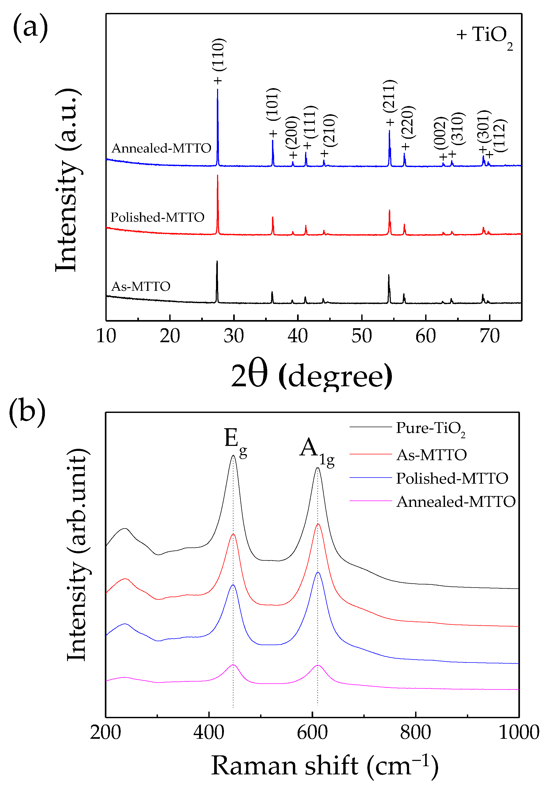
Figure 1. (a) XRD patterns of the as-MTTO, polished MTTO, and annealed MTTO ceramics sintered at 1400 °C for 2 h. (b) Raman spectra of the pure TiO2, as-MTTO, polished MTTO, and annealed MTTO ceramics.
Molecules 26 06952 g001
Figure 2. SEM image of an as-MTTO ceramic sample (a) and FE-SEM mapping images of all elements (b), Ti (c), O (d), Mg (e), and Ta (f).
Molecules 26 06952 g002
Figure 3. Frequency dependence of (a) ε′ and (b) tanδ at RT in as-MTTO, polished MTTO, and annealed MTTO ceramics. The inset of (b) shows the conductivity at RT in the frequency range of 40–106 Hz.
Molecules 26 06952 g003
Figure 4. (a) Temperature dependence of ε′ for as-MTTO and annealed MTTO ceramics at 1 kHz; the inset shows the temperature dependence of the tanδ of the as-MTTO and annealed MTTO ceramics at 1 kHz. (b) Temperature coefficient of ε′ at 1 kHz for as-MTTO and annealed MTTO ceramics. (c) Frequency dependence of ε′ at RT under different DC voltage biases for the annealed MTTO ceramic. (d) DC bias voltage dependence of ε′ at 103 and 104 Hz for the annealed MTTO ceramic.
Molecules 26 06952 g004
Figure 5. Impedance complex plane plots (Z*) for the as-MTTO, polished MTTO, and annealed MTTO ceramics at RT. The inset shows Z* plots of the high frequency data near the origin.
Molecules 26 06952 g005
Table 1. Lattice parameters and Raman shift of pure TiO2 and as-, polished and annealed MTTO ceramics.
SampleLattice Parameters (Å)Raman Shift (cm−1)
acEgA1g
Pure TiO2--447610.0
As-MTTO4.5972.963447611.5
Polished MTTO4.5972.963446.5610.5
Annealed MTTO4.5972.963446.5610.5
Publisher’s Note: MDPI stays neutral with regard to jurisdictional claims in published maps and institutional affiliations.

