
Temperature Dependent Excitonic Transition Energy and Enhanced Electron-Phonon Coupling in Layered Ternary SnS2-xSex Semiconductors with Fully Tunable Stoichiometry

Abstract
:1. Introduction
2. Experimental
3. Results and Discussion
4. Conclusions
Author Contributions
Funding
Data Availability Statement
Acknowledgments
Conflicts of Interest
Sample Availability
References
- Novoselov, K.S.; Geim, A.K.; Morozov, S.V.; Jiang, D.; Zhang, Y.; Dubonos, S.V.; Grigorieva, I.V.; Firsov, A.A. Electric field effect in atomically thin carbon films. Science 2004, 306, 666–669. [Google Scholar] [CrossRef] [PubMed] [Green Version]
- Li, L.; Yu, Y.; Ye, G.J.; Ge, Q.; Ou, X.; Wu, H.; Feng, D.; Chen, X.H.; Zhang, Y. Black phosphorus field-effect transistors. Nat. Nanotechnol. 2014, 9, 372–377. [Google Scholar] [CrossRef] [PubMed] [Green Version]
- Yankowitz, M.; Ma, Q.; Jarillo-Herrero, P.; LeRoy, B.J. van der Waals heterostructures combining graphene and hexagonal boron nitride. Nat. Rev. Phys. 2019, 1, 112–125. [Google Scholar] [CrossRef]
- Tao, L.; Cinquanta, E.; Chiappe, D.; Grazianetti, C.; Fanciulli, M.; Dubey, M.; Molle, A.; Akinwande, D. Silicene field-effect transistors operating at room temperature. Nat. Nanotechnol. 2020, 10, 227–231. [Google Scholar] [CrossRef]
- Wang, Q.H.; Kalantar-Zadeh, K.; Kis, A.; Coleman, J.N.; Strano, M.S. Electronics and optoelectronics of two-dimensional transition metal dichalcogenides. Nat. Nanotechnol. 2012, 7, 699–712. [Google Scholar] [CrossRef]
- Akinwande, D.; Petrone, N.; Hone, J. Two-dimensional flexible nanoelectronics. Nat. Commun. 2014, 5, 5678. [Google Scholar] [CrossRef] [PubMed]
- Akinwande, D.; Huyghebaert, C.; Wang, C.H.; Serna, M.I.; Goossens, S.; Li, L.J.; Philip Wong, H.S.; Koppens, F.H.L. Graphene and two-dimensional materials for silicon technology. Nature 2019, 573, 507–518. [Google Scholar] [CrossRef] [PubMed]
- Mak, K.F.; Lee, C.; Hone, J.; Shan, J.; Heinz, T.F. Atomically thin MoS2: A new direct-gap semiconductor. Phys. Rev. Lett. 2010, 105, 136805. [Google Scholar] [CrossRef] [PubMed] [Green Version]
- Han, H.V.; Lu, A.Y.; Lu, L.S.; Huang, J.K.; Li, H.; Hsu, C.L.; Lin, Y.C.; Chiu, M.H.; Suenaga, K.; Chu, C.W.; et al. Photoluminescence enhancement and structure repairing of monolayer MoSe2 by hydrohalic acid treatment. ACS Nano 2016, 10, 1454–1461. [Google Scholar] [CrossRef] [Green Version]
- He, Z.; Xu, W.; Zhou, Y.; Wang, X.; Sheng, Y.; Rong, Y.; Guo, S.; Zhang, J.; Smith, J.M.; Warner, J.H. Biexciton formation in bilayer tungsten disulfide. ACS Nano 2016, 10, 2176–2183. [Google Scholar] [CrossRef] [PubMed]
- Mitioglu, A.A.; Plochocka, P.; Granados del Aguila, A.; Christianen, P.C.M.; Deligeorgis, G.; Anghel, S.; Kulyuk, L.; Maude, D.K. Optical Investigation of Monolayer and Bulk Tungsten Diselenide (WSe2) in High Magnetic Fields. Nano Lett. 2020, 20, 4387–4392. [Google Scholar] [CrossRef] [Green Version]
- Radisavljevic, B.; Radenovic, A.; Brivio, J.; Giacometti, V.; Kis, A. Single-layer MoS2 transistors. Nat. Nanotechnol. 2011, 6, 147–150. [Google Scholar] [CrossRef] [PubMed]
- Yin, Z.; Li, H.; Li, H.; Jiang, L.; Shi, Y.; Sun, Y.; Lu, G.; Zhang, Q.; Chen, X.; Zhang, H. Single-layer MoS2 phototransistors. ACS Nano 2012, 6, 74–80. [Google Scholar] [CrossRef] [PubMed] [Green Version]
- Li, M.Y.; Shi, Y.; Cheng, C.C.; Lu, L.S.; Lin, Y.C.; Tang, H.L.; Tsai, M.L.; Chu, C.W.; Wei, K.H.; He, J.H.; et al. Epitaxial growth of a monolayer WSe2-MoS2 lateral p-n junction with an atomically sharp interface. Science 2020, 349, 524–528. [Google Scholar] [CrossRef] [PubMed] [Green Version]
- Tsai, M.L.; Su, S.H.; Chang, J.K.; Tsai, D.S.; Chen, C.H.; Wu, C.I.; Li, L.J.; Chen, L.J.; He, J.H. Monolayer MoS2 heterojunction solar cells. ACS Nano 2014, 8, 8317–8322. [Google Scholar] [CrossRef] [PubMed]
- Krasnozhon, D.; Lembke, D.; Nyffeler, C.; Leblebici, Y.; Kis, A. MoS2 transistors operating at gigahertz frequencies. Nano Lett. 2014, 14, 5905–5911. [Google Scholar] [CrossRef] [PubMed] [Green Version]
- Lan, Y.W.; Chen, P.C.; Lin, Y.Y.; Li, M.Y.; Li, L.J.; Tu, Y.L.; Yang, F.L.; Chen, M.C.; Li, K.S. Scalable fabrication of a complementary logic inverter based on MoS2 fin-shaped field effect transistors. Nanoscale Horiz. 2019, 4, 683–688. [Google Scholar] [CrossRef]
- Wachter, S.; Polyushkin, D.K.; Bethge, O.; Mueller, T. A microprocessor based on a two-dimensional semiconductor. Nat. Commun. 2017, 8, 14948. [Google Scholar] [CrossRef] [Green Version]
- Song, H.S.; Li, S.L.; Gao, L.; Xu, Y.; Ueno, K.; Tang, J.; Cheng, Y.B.; Tsukagoshi, K. High-performance top-gated monolayer SnS2 field-effect transistors and their integrated logic circuits. Nanoscale 2013, 5, 9666–9670. [Google Scholar] [CrossRef] [PubMed]
- Su, G.; Hadjiev, V.G.; Loya, P.E.; Zhang, J.; Lei, S.; Maharjan, S.; Dong, P.; Ajayan, P.M.; Lou, J.; Peng, H. Chemical vapor deposition of thin crystals of layered semiconductor SnS2 for fast photodetection application. Nano Lett. 2015, 15, 506–513. [Google Scholar] [CrossRef]
- Guo, C.; Tian, Z.; Xiao, Y.; Mi, Q.; Xue, J. Field-effect transistors of high-mobility few-layer SnSe2. Appl. Phys. Lett. 2016, 109, 203104. [Google Scholar] [CrossRef] [Green Version]
- Pei, T.; Bao, L.; Wang, G.; Ma, R.; Yang, H.; Li, J.; Gu, C.; Pantelides, S.; Du, S.; Gao, H.J. Few-layer SnSe2 transistors with high on/off ratios. Appl. Phys. Lett. 2016, 108, 053506. [Google Scholar] [CrossRef] [Green Version]
- Wei, H.; Su, Y.; Chen, S.; Lin, Y.; Yang, Z.; Chen, X.; Zhang, Y. Novel SnSxSe1-x nanocrystals with tunable band gap: Experimental and first-principles calculations. J. Mater. Chem. 2011, 21, 12605–12608. [Google Scholar] [CrossRef]
- Gupta, R.; Kaur, B.; Carrete, J.; Bera, C. A theoretical model of the thermoelectric properties of SnSxSe1−x and how to further enhance its thermoelectric performance. J. Appl. Phys. 2019, 126, 225105. [Google Scholar] [CrossRef]
- Du, L.; Wang, C.; Xiong, W.; Wei, B.; Yang, F.; Chen, S.; Ma, L.; Wang, X.; Xia, C.; Zhang, X.; et al. Strain-induced band-gap tuning of 2D-SnSSe flakes for application in flexible sensors. Adv. Mater. Technol. 2019, 5, 1900853. [Google Scholar] [CrossRef]
- Perumal, P.; Ulaganathan, R.K.; Sankar, R.; Liao, Y.M.; Sun, T.M.; Chu, M.W.; Chou, F.C.; Chen, Y.T.; Shih, M.H.; Chen, Y.F. Ultra-thin layered ternary single crystals [Sn(SxSe1-x)2] with bandgap engineering for high performance phototransistors on versatile substrates. Adv. Funct. Mater. 2016, 26, 3630–3638. [Google Scholar] [CrossRef]
- Aspnes, D.E. Handbook on Semiconductors; Balkanski, M., Ed.; North-Holland: Amsterdam, The Netherlands, 1980; p. 109. [Google Scholar]
- Yu, J.; Xu, C.Y.; Li, Y.; Zhou, F.; Chen, X.S.; Hu, P.A.; Zhen, L. Ternary SnS2-xSex alloys nanosheets and nanosheet assemblies with tunable chemical compositions and band gaps for photodetector applications. Sci. Rep. 2015, 5, 171709. [Google Scholar] [CrossRef] [PubMed] [Green Version]
- Gonzalez, J.M.; Oleynik, I.I. Layer-dependent properties of SnS2 and SnSe2 two-dimensional materials. Phys. Rev. B 2016, 94, 125443. [Google Scholar] [CrossRef] [Green Version]
- Feng, Q.; Zhu, Y.; Hong, J.; Zhang, M.; Duan, W.; Mao, N.; Wu, J.; Xu, H.; Dong, F.; Lin, F.; et al. Growth of large-area 2D MoS2(1-x)Se2x semiconductor alloys. Adv. Mater. 2014, 26, 2648–2653. [Google Scholar] [CrossRef] [PubMed]
- Fu, Q.; Yang, L.; Wang, W.; Han, A.; Huang, J.; Du, P.; Fan, Z.; Zhang, J.; Xiang, B. Synthesis and enhanced electrochemical datalytic performance of monolayer WS2(1-x)Se2x with a tunable band gap. Adv. Mater. 2015, 27, 4732–4738. [Google Scholar] [CrossRef]
- Wang, D.; Zhang, X.; Guo, G.; Gao, S.; Li, X.; Meng, J.; Yin, Z.; Liu, H.; Gao, M.; Cheng, L.; et al. Large--area synthesis of layered HfS2(1-x)Se2x alloys with fully tunable chemical compositions and bandgaps. Adv. Mater. 2018, 18, 1803285. [Google Scholar] [CrossRef]
- Li, H.; Duan, X.; Wu, X.; Zhuang, X.; Zhou, H.; Zhang, Q.; Zhu, X.; Hu, W.; Ren, P.; Guo, P.; et al. Growth of alloy MoS2xSe2(1-x) nanosheets with fully tunable chemical compositions and optical properties. J. Am. Chem. Soc. 2014, 136, 3756–3759. [Google Scholar] [CrossRef]
- Kudrynskyi, Z.R.; Wang, X.; Sutcliffe, J.; Bhuiyan, M.A.; Fu, Y.; Yang, Z.; Makarovsky, O.; Eaves, L.; Solomon, A.; Maslyuk, V.T.; et al. Van der Waals SnSe2(1-x)S2x alloys: Composition-dependent bowing coefficient and electron–phonon Interaction. Adv. Funct. Mater. 2020, 30, 1908092. [Google Scholar] [CrossRef] [Green Version]
- Wang, Y.; Huang, L.; Li, B.; Shang, J.; Xia, C.; Fan, C.; Deng, H.X.; Wei, Z.; Li, J. Composition-tunable 2D SnSe2(1-x)S2x alloys towards efficient bandgap engineering and high performance (opto)electronics. J. Mater. Chem. C 2017, 5, 84–90. [Google Scholar] [CrossRef]
- O’Donnell, K.P.; Chen, X. Temperature dependence of semiconductor band gaps. Appl. Phys. Lett. 1991, 58, 2924–2926. [Google Scholar] [CrossRef] [Green Version]
- Lantenschlager, P.; Garriga, M.; Logothetidis, S.; Cardona, M. Interband critical points of GaAs and their temperature dependence. Phys. Rev. B 1987, 35, 9174–9189. [Google Scholar] [CrossRef]
- Burton, L.A.; Whittles, T.J.; Hesp, D.; Linhart, W.M.; Skelton, J.M.; Hou, B.; Webster, R.; O’Dowd, G.; Reece, C.; Cherns, D.; et al. Electronic and optical properties of single crystal SnS2: An earth-abundant disulfide photocatalyst. J. Mater. Chem. A 2016, 4, 1312–1318. [Google Scholar] [CrossRef] [Green Version]
- Raadik, T.; Grossberg, M.; Raudoja, J.; Traksmaa, R.; Krustok, J. Temperature-dependent photoreflectance of SnS crystals. J. Phys. Chem. Solids 2013, 74, 1683–1685. [Google Scholar] [CrossRef]


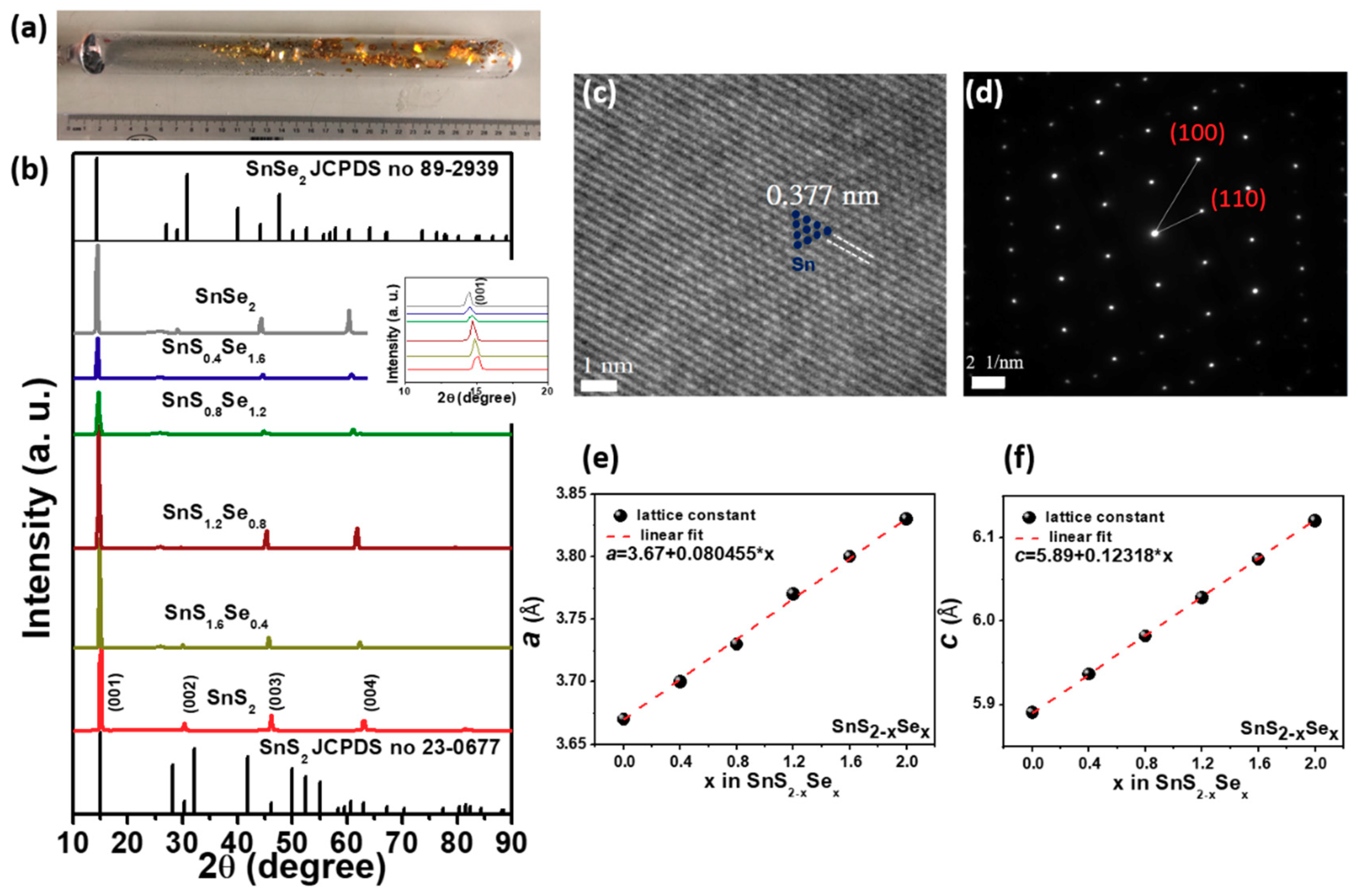
| Measured Composition (%) | Lattice Constant (Å) | ||||
|---|---|---|---|---|---|
| SnS2-xSex | Sn | S | Se | a | c |
| SnS2 | 33.46 | 66.54 | 3.67 ± 0.02 | 5.89 ± 0.02 | |
| SnS1.6Se0.4 | 33.72 | 52.94 | 13.34 | 3.70 ± 0.02 | 5.97 ± 0.02 |
| SnS1.2Se0.8 | 33.94 | 41.38 | 24.68 | 3.73 ± 0.02 | 6.01 ± 0.02 |
| SnS0.8Se1.2 | 33.99 | 27.29 | 38.72 | 3.77 ± 0.02 | 6.05 ± 0.02 |
| SnS0.4Se1.6 | 34.16 | 11.07 | 54.77 | 3.80 ± 0.02 | 6.08 ± 0.02 |
| SnSe2 | 33.79 | 66.21 | 3.83 ± 0.02 | 6.12 ± 0.02 | |
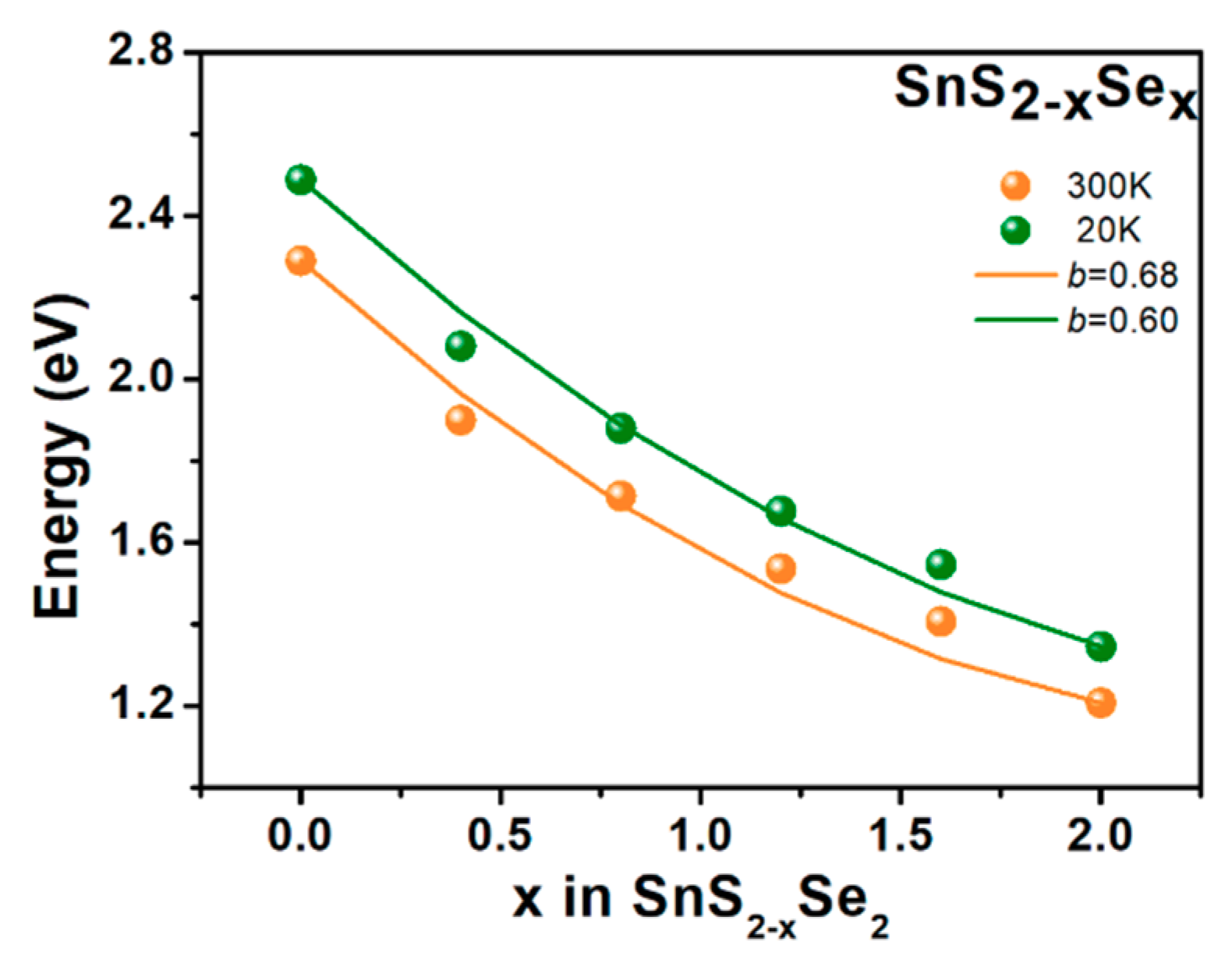
| Material | (eV) | S | <hv> (meV) | (meV) | (meV) | dEex/dT (meV/K) |
|---|---|---|---|---|---|---|
| SnS2 a | 2.490 | 5.18 | 16.3 | 85 | 190 | 0.82 |
| SnS1.6Se0.4 a | 2.075 | 4.46 | 13.2 | 78 | 187 | 0.73 |
| SnS1.2Se0.8 a | 1.880 | 4.32 | 13.1 | 75 | 187 | 0.70 |
| SnS0.8Se1.2 a | 1.679 | 3.48 | 12.3 | 69 | 185 | 0.61 |
| SnS0.4Se1.6 a | 1.554 | 3.45 | 11.6 | 67 | 183 | 0.58 |
| SnSe2 a | 1.346 | 3.32 | 10.1 | 64 | 183 | 0.56 |
| SnS2 b | 2.559 | 5.76 | 26 | 151 | 304 | |
| SnS2 c | 2.34 | 7.0 | 32.2 | 81 | 189 | |
| SnS1.4Se0.6 c | 1.80 | 4.5 | 27.8 | 71 | 201 | |
| SnSe2 c | 1.31 | 3.0 | 18.4 | 60 | 213 | |
| SnS d | 1.375 | 1.86 | 24.3 | 41 | 270 |
Publisher’s Note: MDPI stays neutral with regard to jurisdictional claims in published maps and institutional affiliations. |
© 2021 by the authors. Licensee MDPI, Basel, Switzerland. This article is an open access article distributed under the terms and conditions of the Creative Commons Attribution (CC BY) license (https://creativecommons.org/licenses/by/4.0/).
Share and Cite
Lin, D.-Y.; Hsu, H.-P.; Tsai, C.-F.; Wang, C.-W.; Shih, Y.-T. Temperature Dependent Excitonic Transition Energy and Enhanced Electron-Phonon Coupling in Layered Ternary SnS2-xSex Semiconductors with Fully Tunable Stoichiometry. Molecules 2021, 26, 2184. https://doi.org/10.3390/molecules26082184
Lin D-Y, Hsu H-P, Tsai C-F, Wang C-W, Shih Y-T. Temperature Dependent Excitonic Transition Energy and Enhanced Electron-Phonon Coupling in Layered Ternary SnS2-xSex Semiconductors with Fully Tunable Stoichiometry. Molecules. 2021; 26(8):2184. https://doi.org/10.3390/molecules26082184
Chicago/Turabian StyleLin, Der-Yuh, Hung-Pin Hsu, Chi-Feng Tsai, Cheng-Wen Wang, and Yu-Tai Shih. 2021. "Temperature Dependent Excitonic Transition Energy and Enhanced Electron-Phonon Coupling in Layered Ternary SnS2-xSex Semiconductors with Fully Tunable Stoichiometry" Molecules 26, no. 8: 2184. https://doi.org/10.3390/molecules26082184
APA StyleLin, D.-Y., Hsu, H.-P., Tsai, C.-F., Wang, C.-W., & Shih, Y.-T. (2021). Temperature Dependent Excitonic Transition Energy and Enhanced Electron-Phonon Coupling in Layered Ternary SnS2-xSex Semiconductors with Fully Tunable Stoichiometry. Molecules, 26(8), 2184. https://doi.org/10.3390/molecules26082184