Article

A Systematical Study on Bands and Defects of CsBX3 (B = Pb, Sn, Ge, X = Cl, Br, I) Perovskite Based on First Principles

1
Beijing Key Laboratory for Sensor, Beijing Information Science and Technology University, Beijing 100101, China
2
School of Applied Science, Beijing Information Science and Technology University, Beijing 100101, China
3
State Key Laboratory on Integrated Optoelectronics, Institute of Semiconductors, Chinese Academy of Sciences, Beijing 100083, China
*
Authors to whom correspondence should be addressed.
Molecules 2024, 29(11), 2479; https://doi.org/10.3390/molecules29112479
Submission received: 1 April 2024 / Revised: 9 May 2024 / Accepted: 14 May 2024 / Published: 24 May 2024

Abstract

:
Metal halide perovskites have attracted considerable attention as novel optoelectronic materials for their excellent optical and electrical properties. Inorganic perovskites (CsPbX3, X = Cl, Br, I) are now viable alternative candidates for third-generation photovoltaic technology because of their high photoelectric conversion efficiency, high carrier mobility, good defect tolerance, simple preparation method and many other advantages. However, the toxicity of lead is problematic for practical implementation. Thus, the fabrication of lead-free perovskite materials and devices has been actively conducted. In this work, the energy band and photoelectric properties of inorganic perovskites CsBX3 (B = Pb, Sn, Ge, X = Cl, Br, I) have been investigated with the first principles calculation, and the possible defect energy levels and their formation energies in different components, in particular, have been systematically studied. The advantages and disadvantages of Sn and Ge as replacement elements for Pb have been demonstrated from the perspective of defects. This study provides an important basis for the study of the properties and applications of lead-free perovskites.

1. Introduction

Perovskites are very important photoelectric materials. Due to their characteristics of high chromatography purity, suitable tunable band gap, high photoluminescence quantum yield and high carrier mobility [1,2,3,4,5], they have been intensively studied in the application of high-efficiency light-emitting diodes, solar cells, detectors and other fields [6,7,8,9,10]. Perovskite was first applied to solar cells in 2009 with an initial power conversion efficiency of only 3.8% [11], and this number has exceeded 25% after a development of more than ten years [12,13]. However, as a heavy metal ion, Pb2+ may harm human health and cause soil pollution [6], which brings toxicity problems that cannot be ignored, and various countries have introduced restrictions on lead. Therefore, lead-free perovskite materials with excellent characteristics have become an important direction for researchers.
ABX3 structure is the most typical of perovskite compositions, among which the stability of pure inorganic perovskites is more prominent, and the most common one is CsPbX3 (X = Cl, Br, I). Replacing Pb2+ in CsPbX3 with non-toxic metal cations with similar ionic radii and properties is a good method to solve the toxicity of perovskite materials. Wu et al. reported Ge-based perovskite nanocrystals synthesized by the solution method for the first time in 2018 [14]. They also investigated the electron beam-induced transformations of CsGeI3 and found a distinctive transformation path compared to heavier Pb atoms in lead halide perovskite NCs. To improve the poor stability of lead-free perovskite, Kang et al. highlight the significant effect of Sn-II precursors used in the synthesis of the resultant CsSnX3 NCs. Stable CsSnX3 NCs can be obtained with the use of antioxidative SnC2O4 as the Sn-II precursor for the strong antioxidative ability of the oxalate ion [15]. In addition to lead-free perovskite materials, their related applications have also received attention from scientists. High-quality Cs3Bi2I9 perovskite nanosheets have been prepared and used in solar cells [16], and it has been proved that Bi-based perovskites have more similar properties with Pb-based ones and also have high quantum yields compared to other nontoxic ions [17,18]. Sun et al. developed new fullerene derivatives as electron transporter layers, and found that the chemical structures of the regioisomers not only affect their energy levels, but also lead to significant differences in their molecular packings and interfacial contacts [19]. They reported an efficiency of 14.30%, representing one of the best performances of Sn-based perovskite solar cells. Lead-free perovskites have also shown great promise for the photochemical conversion of CO2 [20,21,22]. However, the fast carrier recombination rates and inadequate adsorption/activation for CO2 molecules have seriously restricted their practical application. Qian et al. developed an innovative Cs2CuBr4/TiO2 photocatalyst by embedding Cs2CuBr4 PQDs in a mesoporous TiO2 matrix, which delivered the CO2 reduction activity to 3.1 and 16.0 times higher than those achieved by pure Cs2CuBr4 and TiO2, respectively [21].
Better defect property is one of the most important advantages of Pb-based perovskites compared to other optoelectronic materials, which is of great significance to the material properties as well as the performance of optoelectronic devices. Generally, in optoelectronic devices, deep-energy-level defects mainly act as recombination centers, shorten the lifetime of minority carriers and reduce the device efficiency, while shallow-energy-level defects are mainly donor or acceptor, which mainly provide carriers and induce the yield of the device. In addition to the location of the energy level, the formation energy is also an important influence factor for the defect concentration. For Pb-based perovskite, such as MAPbI3, most of the defects (Ii, MAPb, VMA, VPb, MAi, PbMA, VI and MAI) are located above the conduction band minimum (CBM) or below the valence band maximum (VBM), forming shallow defect energy levels, and meanwhile have relatively low formation energies, resulting in higher concentrations. However, for a few other defects (IMA, IPb, Pbi and PbI), they are located in the middle of the forbidden band and form deep defect energy levels. Fortunately, their relatively higher formation energies ensure lower concentrations and less impact [23,24]. This is the reason why Pb-based perovskites have better defect tolerance [23,25]. It is hoped that lead-free perovskites will have similar properties so as to minimize the negative effects of defects.
CsSnI3 is an early proposed lead-free perovskite material, and there have been many reports on the research of its defects. In 2012, Chung et al. made a computational study of several point defects in CsSnI3 and found that the Sn vacancies mainly act as p-type carrier sources and have lower formation energies. Thermal-activated Sn vacancies improve conductivity and PL intensity of CsSnI3 [26]. Xu et al. further investigated the possible defects in CsSnI3 to verify the intrinsic defect energy level distribution in CsSnI3 [27]. It was shown that all the transfer energy levels of the acceptor defects are below the VBM and will all ionize once formed, increasing the carrier concentration. Among the donor defects, SnI is the only deep-energy-level defect that will exist as a recombination center of carriers, whose density can be reduced by increasing the concentration of Sn in the precursor. The intrinsic defects of MASnxPb1−xI3 were also studied with first principles calculations [28]. It was found that three defects (Ii, VSn, and VPb) have a large impact on the carrier lifetime. Ii introduces a deep defect state in the forbidden band and leads to a significant decrease in carrier lifetime and PL intensity, which fortunately can be effectively avoided by reducing the anion content. Neither VSn nor VPb produce defect energy in the band gap; however, they can cause changes in the energy dispersions of VBM and CBM, which in turn change the carrier mobility and lifetime. Although the previous reports on the defect properties of lead-free perovskite have important guiding significance, most of them only focus on several single materials, and the results are not comprehensive enough. Here, we have specifically conducted a systematic and comprehensive study of all the possible point defects in Sn- and Ge-based perovskites CsBX3 (B = Pb, Sn, Ge, X = Cl, Br, I), the two optimally desired replacement elements for Pb, and studied the distribution of defect energy levels for different metal and halogen elements.
In this paper, CsBX3 (B = Pb, Sn, Ge, X = Cl, Br, I) perovskites are investigated by first principles calculations. The electronic properties of perovskites, including energy band structure, density of states (DOS), and absorption coefficients, are firstly studied. On this basis, the energy level and distribution of all possible point defects are explored in depth to analyze the defect tolerance of the material. Finally, the DOS distribution of the defect lattice is calculated, which can explain the influence of defect location on carrier concentration well. This study work not only reveals the mechanisms of the defects’ existence and their effect on the material optoelectronic properties, but also provides experience on the experimental preparation of different materials, and the prediction of the device performance with different materials.

2. Models and Calculation Methods

At room temperature, CsBX3 perovskite is cubic crystal and the space group is Pm-3m. The unit cell contains five atoms in a single formula unit, and the positions with fractional coordinates (0.00, 0.00, 0.00), (0.50, 0.50, 0.50), and (0.00, 0.50, 0.50) are occupied by Cs, B, and X atoms, respectively. B2+ and its coordinated X form an octahedral, B2+ is the center of the octahedral structure, and X is located at the top corner of the octahedron. A unit cell is shown in Figure 1a. There are three types of point defects in the cell, namely substitution, vacancy and gap, and Figure 1b–d show one cell structure for each type of defect, respectively.
Here, the valence electronic configurations of the atoms are as follows: Cs: 5s25p66s1, Pb: 3d64s2, Sn: 5s25p2, Ge: 4s24p2, Cl: 3s23p5, Br: 4s24p5, I: 5s25p5. The Perdew–Burke–Ernzerhof functional for solids (PBE) within the generalized gradient approximation (GGA) was used to describe the exchange correlation interaction between the valence electrons. As the major computational parameters, the plane-wave cutoff energy was set to 405 eV, and the Monkhorst–Pack special k points were set to (6 × 6 × 6) for structural relaxations and electronic structure calculations. To obtain more reliable band gaps, we also performed electronic structure calculations using the Heyd–Scuseria–Ernzerhof (HSE06) hybrid functional, in which we replaced 25% of the PBE exchange functional with the exact Hartree–Fock exchange functional, providing bulk band gaps in good agreement with the experiment. Subsequently, the light absorption capacity of the material was also calculated.
To study the distribution of point defects in perovskite, we calculated the energy level locations and formation energies of all possible defects formed in CsBX3, including vacancy, substitution and interstitial. For a defect α with charged state q, the formation energy ΔH (α, q) is calculated as shown below:
ΔH (α, q) = E (α, q) − E (host) + ∑iniμi + q [EVBM (host) + Ef + ∆V]
where E (α, q) is the energy of the supercell with defect α in ionization state q, E (host) is the energy of the supercell without defect, ni is the number of atoms added or lost from defect α, μi is the chemical potential of the corresponding element, EVBM (host) is the energy at the VBM of the supercell without defect, and Ef is the Fermi energy relative to EVBM (host), i.e., Ef = 0 at the position of EVBM (host), ∆V = V (α, q, R) − V (host, R), where R is the farthest position from the defect. Here, the formation energy of the defect is calculated with PBE generalization. However, the PBE calculation underestimates the formation energy per electron ∆CBM when there are electrons occupying the host energy level (when there are holes occupying the host energy level, the PBE calculation underestimates the formation energy per hole ΔVBM) [29], so we added the difference in the conduction (valence) band edge energy generated by HSE06 to correct the defect formation energy calculated by PBE.

3. Discussion

3.1. ABX3 Crystal Structure
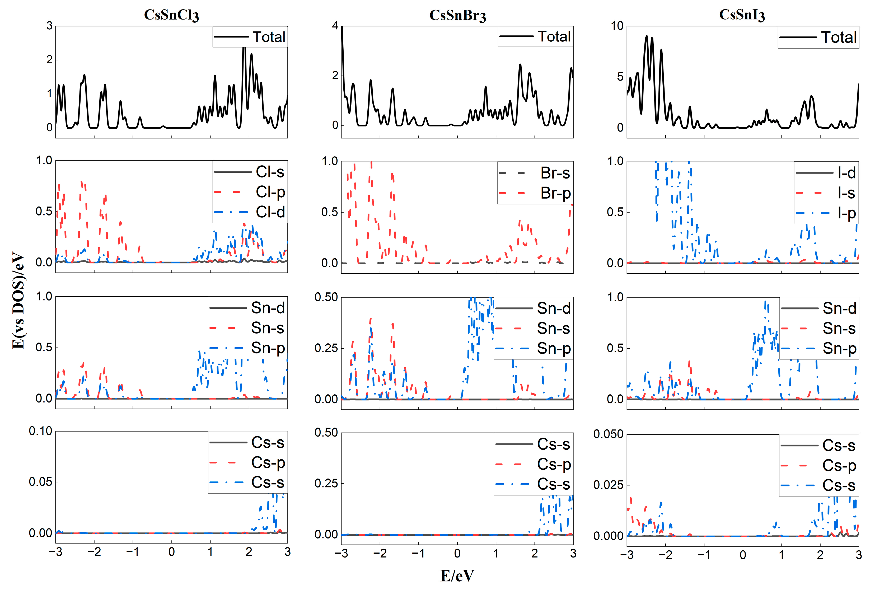
As a preliminary test of the formability of perovskite structures, the Goldschmidt tolerance factor tG was first analyzed, and the calculation formula is shown in Formula (2):
tG = (rA + rX)/(21/2 (rB + rX))
where rA represents the ionic radius of A, rB represents the ionic radius of B, and rX represents the ionic radius of X. When the calculated result is in the range of 0.8~1.0, it can support the formation of perovskite structure in a stable phase [30]. After the cell is established, the relaxation calculation is carried out to optimize the structure. Table 1 shows the lattice parameters and tolerance factors of the perovskite materials studied thereinafter.
It can be seen from the table that the lattice constants of the perovskites with the same B element gradually increase when the X elements are Cl, Br and I in order, the lattice constants of the perovskites with the same X element also gradually increase when the B elements are Ge, Sn, and Pb in order, which is consistent with the change in ionic radii of the constituent elements. The tolerance factors of all nine materials are in the range of 0.8~1.0, which ensures the formation of the perovskite structure.

3.2. Band Strucure

The energy band is the fundamental factor that determines the optoelectronic properties of semiconductor materials. We calculated the energy bands of CsBX3 (B = Pb, Sn, Ge, X = Cl, Br, I) after relaxation, and the PBE and HSE06 software packages were used, respectively, to explore the details of the electronic structure. Since the ABX3 perovskite belongs to the Pm-3m space group, we selected the high symmetry point paths in the Brillouin zone as X (0.50, 0.00, 0.00)-R (0.50, 0.50, 0.50)-M (0.50, 0.50, 0.00)-T (0.00, 0.00, 0.00)-R (0.50, 0.50, 0.50). The band gaps of the materials are summarized in Table 2. The band gap obtained from the PBE generalized function calculation is severely underestimated compared to the experimental value, which is consistent with the previous theoretical results [30]. This underestimation of the band gap becomes more severe as the halogen atoms become lighter when changing from I to Cl due to weaker relativistic effects [30]. The HSE06 hybridization generalization significantly improves this defect and yields a band gap closer to the experimental value due to a fraction of screened Hartree–Fock exchange included in HSE06, which improves the discontinuity in the Kohn–Sham potential derivative for integer numbers of electrons.
The energy band structures obtained by the HSE06 hybridization generalization calculation are given in Figure 2. Sn-, Ge- and Pb-based perovskites have similar energy band structures. They all have direct band gaps, the inverse spatial coordinates of the CBM and VBM are located at the R (0.50, 0.50, 0.50), and the band formation and order are similar. This is because the chemical composition and the backbone structure formed by B and X are similar. The direct band gap structure makes it easier for the carrier transition from the VBM to the CBM generated by photons without the assistance of phonons, and facilitates the generation of photogenerated carriers, which makes Sn- and Ge-based perovskites equally promising for the application of high-efficiency optoelectronic devices. The band gap decreases with increasing halogen ion radius from Cl to I, which has been demonstrated in previous work, and provides a classical way to regulate the band gap by controlling the halogen composition [40,41]. This may be because the longer B-X bonds weaken the interaction between B and X orbitals, leading to a narrowing of the band gap while causing lattice expansion [42,43]. The effect of B elements on the band gap is significant and more complex, which cannot be explained well by bond length alone and needs to be further investigated.
The DOS distribution is another important parameter for studying the properties of optoelectronic materials, as it reveals the contribution of material composition elements to the energy bands and distribution of charge carriers. Here, the DOS of the above CsBX3 is calculated. The results are shown in Figure 3. It can be observed that the VBM mainly originates from the p orbitals of X and a small amount of s orbitals of B, while the CBM is mainly composed of the p orbitals of B and a small amount of p and d orbitals of X. Their overlap indicates significant hybridization between each other. That is, the band gap is mainly determined by the B and X elements, and the contribution of the A (Cs) is negligible, which is why changing the elements in the A-site has little effect on the band gap of the material [1]. This is consistent with the conclusion in Figure 2.
A high absorption coefficient is critical for efficient photoelectric conversion of the material. The absorption coefficient of perovskite is derived from the real and imaginary parts of the dielectric function together. It is calculated as α(ω) = 21/2e/ħc [(ε1222)1/2 − ε1]1/2α, where ε1(ω) and ε2(ω) are the real and imaginary parts of the dielectric function, respectively, and ω is the frequency of the photon [44].
The light absorption spectra of the nine materials are given in Figure 4. It can be found that when B changes from Pb to Ge, the absorption edge gradually produces a red shift, and for the same B-site element, when X is Cl, Br and I elements, the absorption curve also shows a more obvious red shift in turn, which corresponds to the size of the band gap. They all have good absorption ability in the visible range, while the Ge- and Sn-based perovskites also have some absorption ability in the infrared region, giving them greater advantages in expanding the absorption scope. Secondly, the absorption peaks of the same B-element materials become larger in the order of X for Cl, Br, and I, which is consistent with the variation in the absorption scope.

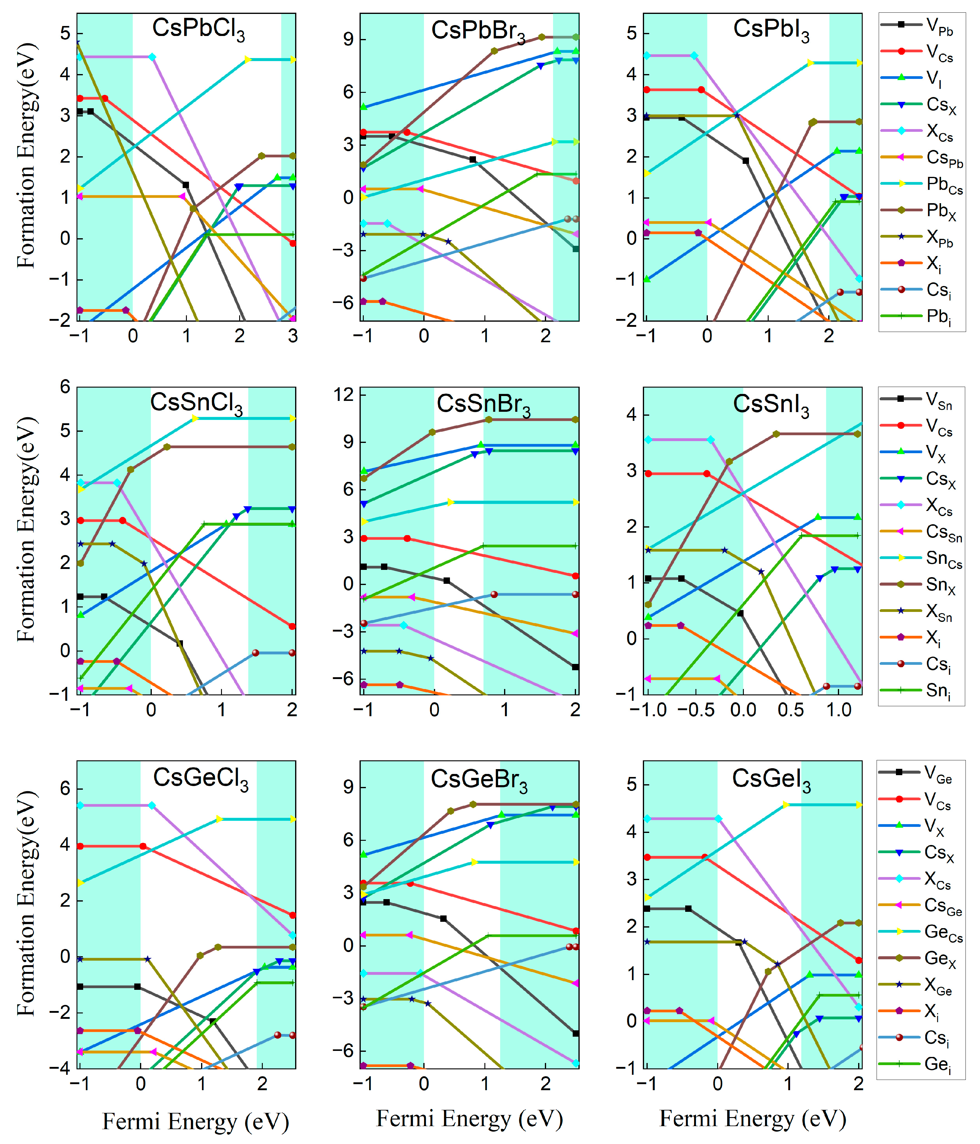
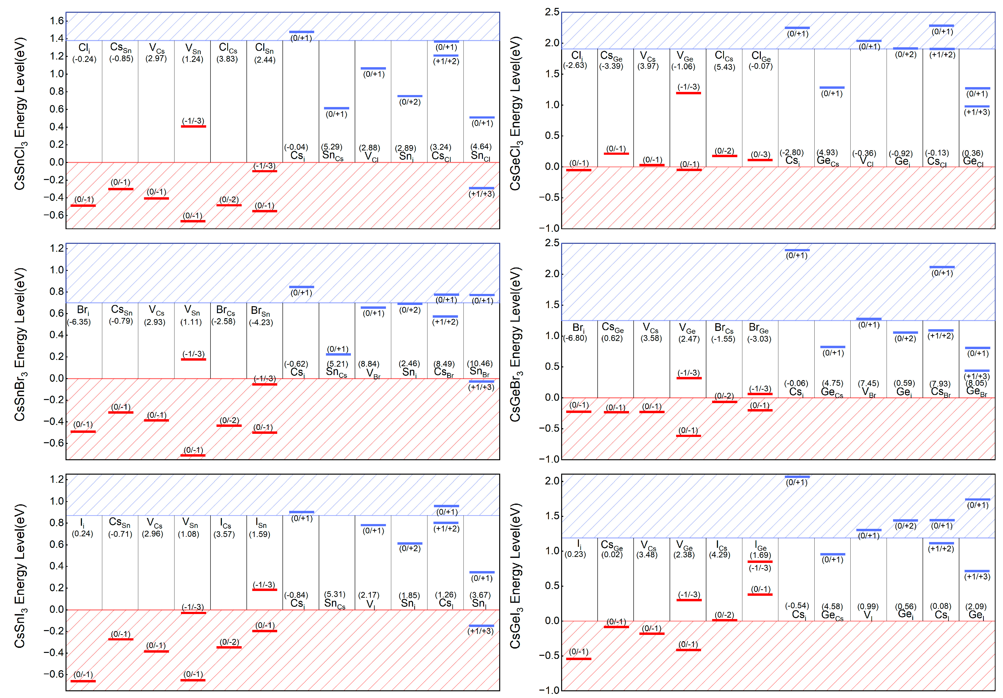
3.3. Defect Property

The properties of defects in absorbers, especially point defects, play a critical role in determining the electron–hole diffusion length and Voc of a solar cell. Defects that create deep levels usually act as Shockley–Read–Hall nonradiative recombination centers and are responsible for short minority carrier lifetime and, thus, low Voc. In contrast, defects with energy levels above the CBM or below the VBM can increase the carrier concentration and improve the efficiency of the device. The defect formation energy is a very important reference to understand the defects’ distribution in semiconductor materials. The higher the formation energy, the lower the chance of defect formation, and also its concentration in the material. Here, we take the calculation result of SnI (Sn substitution of I) defect in CsSnI3 as an example, to describe the significance of the defect formation energy curve calculated by first principles. SnI may exist in three charged states, i.e., electrically neutral, with +1 charge, and with +3 charge. The formation energy in each charged state is calculated in accordance with Equation (1), and the results are shown in Figure 5. The formation energy of neutral defects does not vary with the Ef, while that of charged defects (SnI1+ and SnI3+) increases with increasing Ef (the slope of the curve is equal to the charge number of the defect), which also applies to those negatively charged acceptor defects. Only the charged state with the lowest formation energy can exist at any Fermi energy, so the actual formation energy curve is composed of section a for electrically neutral state, section b for +1 charged state and section c for +3 charged state. According to Equation (1), the formation energy versus Fermi energy for all possible defects in ABX3 perovskites were predicted, including VCs (Cs vacancy), VB, VX, CsB (Cs substitution of B), BCs, CsX, XCs, BX, XB, Csi (Cs gap), Bi and Xi, and the calculation results are shown in Figure 6.
In order to better observe the changes in formation energy, we have listed the two maximum and minimum formation energies of each donor and acceptor defect for nine materials, as shown in Table 3, Table 4, Table 5 and Table 6. It can be clearly seen that the formation energy of defect is much more influenced by X element than by B element. Because the generated defects can have a significant impact on the material, we focus more on the donor and acceptor defects with lower formation energies. In most materials, Csi and Bi are the donor defects with the lowest formation energy, but when X is I, CsX replaces the position of Bi. This is easy to understand, because the Cs ions do not participate in the skeletal structure that constitutes the perovskite, but rather fill the octahedral structure composed of metal and halogen ions, making them subject to the least binding forces and more likely to form defects, which agrees with the previous conclusions [23]. Due to the larger ionic radius of I, it is more easily replaced by Cs, making the formation energy of CsI relatively low. For the acceptor defects, CsB and Xi have relatively low formation energies for CsPbCl3 and CsPbI3, while XB becomes more easily formed in CsPbBr3. It is believed that the difference in the compounds containing Br ions is caused by multiple factors. Due to the low local symmetry of the X site, the 5p orbital of B splits forms a shallow energy level near the CBM, but also a deep energy level in the forbidden band [27]. Although the three halogen atoms have similar electronic structures and also orbital couplings with B ions, the coupling strength of Cl with B is stronger due to a smaller atomic radius, while those of Br and I will gradually weaken as the atomic radius increases. On the other hand, as discussed above, the radius of the ion plays a key role in the stability of the compound structure and the formation of defects. Cl ions with smaller radii do not have an advantage in forming stable compounds, while Br and I can form more stable compounds with fewer defects as the ion radius increases. The balance and contest between these two factors make it easier for the intermediate Br to escape or to be replaced by other ions, forming vacancy or substitution defects, which results in the conclusion we finally obtained. This is consistent with the research results of W. Swift et al., that Bri in CsPbBr3 is a deep-level defect with a high concentration [45].
Ionization is an important parameter for determining the contribution of defect in carrier concentration, which is mainly influenced by their transition energy levels. The transition energy level εα(q/q’) is defined as the Fermi energy level when defect α with two different charge states q and q’ have the same formation energy [46], and they are located at the turning points in the formation energy diagram, where the defects can release electrons or holes and change their charge state from q to q’. For example, the Fermi energy level Ef = −0.66 eV corresponds to the transition point of the Ii from the electroneutral to the −1-valence state in the CsSnI3 system, so that its (0/−1) transition energy level is located at 0.66 eV below the VBM. Based on this approach, the positions of the transition energy levels of defects in Sn- and Ge-based perovskites are plotted in Figure 7. The formation energy and the energy level are the two main factors determining the distribution of a defect in the material. The acceptor defect with a transition energy level below the VBM or the donor defect with a transfer energy level above the CBM will ionize once formed, increasing the concentration of carriers. However, if the transition energy level of the defect lies in the forbidden band, the defect will then act as a carrier trap and recombination center for the photogenerated electron–hole pair, decreasing the carrier concentration.
Many previous studies have pointed out that the good defect property is one of the important reasons why Pb-based perovskites are sought after by scholars for optoelectronic device applications [23,47,48]. Most of the defects in Pb-based perovskites have shallow energy levels, and the formation energy of the very few with deep energy levels is relatively higher, meaning they are difficult to form and they affect the performance of the material vary little [23,49].
Fortunately, the defect properties of Sn-based perovskites are similar to those of Pb-based ones. Almost all of the acceptor defect transition energy levels in CsSnX3 are below the VBM, which means they will all ionize once formed. This conclusion is similar to that of a previous study [27]. Each ionized defect produces the same number of carriers as the amount of charge in its ionized state. Therefore, a high concentration of shallow-energy-level defects causes a higher concentration of carriers and further conductivity of the material. Although there are some deep-energy-level donor and acceptor defects, such as SnCs, VCl, CsCl, SnCl in CsSnCl3, their formation energies are relatively high, hindering the mass formation of recombination centers. At the same time, it is important to note that defects cannot capture two electrons or holes at the same time [50,51], which means that transfer energy levels like (−1/+1), (−2/0), and (0/+2) that produce transitions of two or more charge states are actually not related to nonradiative recombination. Therefore, VSn and Sni are not actually nonradiative recombination centers.
In contrast, the performance of Ge-based perovskites is not so satisfactory. A number of deep-energy-level defects with low formation energies (CsGe, VGe, ClGe and GeCl in CsGeCl3, Gei in CsGeBr3, and CsI in CsGeI3) provide conditions for the existence of carrier recombination centers. CsGeI3 and CsGeBr3 are significantly more tolerant to defects than CsGeCl3, but undesirable defects exist in both of them as well. The defect properties of Sn- and Ge-based halide perovskites explained the advantages of Sn as the substitute for Pb, and the rapid growth of Sn-based perovskite compared with Ge-based ones.
The DOS in crystals, including those of defects that are studied here, to investigate the influence of defect energy levels and formation energies on carrier contribution. Two defects (CsSn and SnCs in CsSnCl3) are studied as a special case, for they are typical ones with shallow and deep energy levels, respectively, and their effect on the carrier state density can specifically illustrate the influence of most defects on carrier concentration and mobility in crystals. The results are shown in Figure 8. It can be clearly observed that CsSn caused complete ionization, which resulted in a higher DOS below the VBM, and increased the carrier concentration in the crystal, while for deep-energy-level defect SnCs, a recombination center was created in the middle of the forbidden band, which is consistent with our previous analysis.

4. Conclusions

The article presents a systematic and comprehensive study of the photoelectric properties of CsBX3 (B = Pb, Sn, Ge. X = Cl, Br, I.) perovskites, especially the properties of defect energy levels and formation energies, based on the first principle calculations. There is a significant effect of B and X elements on the band gap, while the effect of Cs elements on the band gap is small. The perovskites constructed with different B-site elements have good absorption ability in the visible range, while the absorption edges of the Ge- and Sn-based perovskites show different degrees of red-shift, which makes them also have some absorption in the infrared region and expands the wavelength range for material applications.
The defect energy levels and formation energies of all possible point defects in CsBX3 (B = Pb, Sn, Ge, X = Cl, Br, I) perovskite are systematically investigated. Sn-based perovskites have similar defect properties with Pb-based material, where most of the defects are near the CBM or the VBM, and form shallow-energy-level defects. For a few defects (SnCs, VCl, SnCs, CsCl and SnCl) existing in the middle of the forbidden band, high formation energies ensure their low concentration, which proves the mobility of Sn-based perovskite and makes it a promising lead-free material. In contrast, there are some defects with deep energy levels in Ge-based perovskites (GeCl in CsGeCl3, Gei in CsGeBr3, and CsI in CsGeI3) with relatively lower formation energies, forming carrier capture centers and hindering their application in optoelectronic devices. These analysis results indicate that Sn has more advantages in defect tolerance when replacing Pb to become an efficient perovskite optoelectronic material. This is the main reason why Sn-based perovskite devices are superior to Ge-based ones. This work is of great significance for the study of lead-free perovskites and provides a basis for theoretical and experimental studies of lead-free perovskites and devices.

Author Contributions

Conceptualization, C.Z. and W.H.; methodology, W.H. and H.W.; software, W.H.; validation, C.Z. and H.W.; formal analysis, H.W.; investigation, C.Z. and H.W.; resources, J.C.; data curation, C.Z. and H.W.; writing—original draft preparation, H.W.; writing—review and editing, C.Z. and W.H.; visualization, C.Z.; supervision, W.H.; project administration, J.C. and Y.Z.; funding acquisition, C.Z. and W.H. All authors have read and agreed to the published version of the manuscript.

Funding

This research was funded by the National Natural Science Foundation of China (No. 61901009 and No. 61875186), State Key Laboratory of Advanced Optical Communication Systems Networks of China (No. 2021GZKF002), Beijing Key Laboratory for Sensors of BISTU (No. 2019CGKF007) and the Key Training Program of the Research Level Improvement Plan of Beijing Information Science and Technology University (No. 2020KYNH222).

Institutional Review Board Statement

Not applicable.

Informed Consent Statement

Not applicable.

Data Availability Statement

The data that support the findings of this study are available from the corresponding author upon reasonable request.

Conflicts of Interest

The authors declare no conflicts of interest.

References

  1. Mao, X.; Sun, L.; Wu, T.; Chu, T.S.; Deng, W.Q.; Han, K.L. First-Principles Screening of All-Inorganic Lead-Free ABX3 Perovskites. J. Phys. Chem. C 2018, 122, 7670–7675. [Google Scholar] [CrossRef]
  2. Kshirsagar, B.; Jaykhedkar, N.; Jain, K.; Kishor, S.; Shah, V.; Ramaniah, L.M.; Tiwari, S. Green CsSnX3 (X = Cl, Br, I)-Derived Quantum Dots for Photovoltaic Applications: First-Principles Investigations. J. Phys. Chem. C 2021, 125, 2592–2606. [Google Scholar] [CrossRef]
  3. Guo, H.; Yoon, G.W.; Li, Z.J.; Yun, Y.; Lee, S.W.; Seo, Y.H.; Jeon, N.J.; Han, G.S.; Jung, H.S. In Situ Polymerization of Cross-Linked Perovskite-Polymer Composites for Highly Stable and Efficient Perovskite Solar Cells. Adv. Energy Mater. 2024, 14, 2302743. [Google Scholar] [CrossRef]
  4. Ali, L.; Ahmad, M.; Shafiq, M.; Zeb, T.; Ahmad, R.; Maqbool, M.; Ahmad, I.; Jalali-Asadabadi, S.; Amin, B. Theoretical studies of CsSnX3 (X= Cl, Br and I) for energy storage and hybrid solar cell applications. Mater. Today Commun. 2020, 25, 101517. [Google Scholar] [CrossRef]
  5. Milstein, T.J.; Kroupa, D.M.; Gamelin, D.R. Picosecond quantum cutting generates photoluminescence quantum yields over 100% in ytterbium-doped CsPbCl3 nanocrystals. Nano Lett. 2018, 18, 3792–3799. [Google Scholar] [CrossRef] [PubMed]
  6. Lin, W.; Hu, X.; Mo, L.; Jiang, X.; Xing, X.; Shui, L.; Priya, S.; Wang, K.; Zhou, G. Progresses on Novel B-Site Perovskite Nanocrystals. Adv. Opt. Mater. 2021, 9, 2100261. [Google Scholar] [CrossRef]
  7. Zhao, Y.; Ma, F.; Qu, Z.H.; Yu, S.Q.; Shen, T.; Deng, H.X.; Chu, X.B.; Peng, X.X.; Yuan, Y.B.; Zhang, X.W.; et al. Inactive (PbI2)2RbCl stabilizes perovskite films for efficient solar cells. Science 2022, 377, 531–534. [Google Scholar] [CrossRef] [PubMed]
  8. Gao, Y.; Ren, F.M.; Sun, D.R.; Li, S.B.; Zheng, G.H.J.; Wang, J.A.; Raza, H.; Chen, R.; Wang, H.X.; Liu, S.W.; et al. Elimination of unstable residual lead iodide near the buried interface for the stability improvement of perovskite solar cells. Energy Environ. Sci. 2023, 16, 2295–2303. [Google Scholar] [CrossRef]
  9. Li, J.H.; Du, P.P.; Guo, Q.X.; Sun, L.; Shen, Z.X.; Zhu, J.X.; Dong, C.; Wang, L.; Zhang, X.; Li, L.Y.; et al. Efficient all-thermally evaporated perovskite light-emitting diodes for active-matrix displays. Nat. Photonics 2023, 17, 435–441. [Google Scholar] [CrossRef]
  10. Zhou, Y.; Fei, C.B.; Uddin, M.A.; Zhao, L.; Ni, Z.Y.; Huang, J.S. Self-powered perovskite photon-counting detectors. Nature 2023, 616, 712–718. [Google Scholar] [CrossRef]
  11. Kojima, A.; Teshima, K.; Shirai, Y.; Miyasaka, T. Organometal Halide Perovskites as Visible-Light Sensitizers for Photovoltaic Cells. J. Am. Chem. Soc. 2009, 131, 6050–6051. [Google Scholar] [CrossRef] [PubMed]
  12. Gao, H.; Xiao, K.; Lin, R.; Zhao, S.; Wang, W.; Dayneko, S.; Duan, C.; Ji, C.; Sun, H.; Bui, A.D.; et al. Homogeneous crystallization and buried interface passivation for perovskite tandem solar modules. Science 2024, 383, 855–859. [Google Scholar] [CrossRef] [PubMed]
  13. Zhou, J.; Tan, L.; Liu, Y.; Li, H.; Liu, X.; Li, M.; Wang, S.; Zhang, Y.; Jiang, C.; Hua, R.; et al. Highly efficient and stable perovskite solar cells via a multifunctional hole transporting material. Joule, 2024; in press. [Google Scholar] [CrossRef]
  14. Wu, X.; Song, W.; Li, Q.; Zhao, X.; He, D.; Quan, Z. Synthesis of Lead-free CsGeI3 Perovskite Colloidal Nanocrystals and Electron Beam-induced Transformations. Chem.—Asian J. 2018, 13, 1654–1659. [Google Scholar] [CrossRef] [PubMed]
  15. Kang, C.; Rao, H.; Fang, Y.; Zeng, J.; Pan, Z.; Zhong, X. Antioxidative Stannous Oxalate Derived Lead-Free Stable CsSnX3 (X=Cl, Br, and I) Perovskite Nanocrystals. Angew. Chem. Int. Ed. 2021, 60, 660–665. [Google Scholar] [CrossRef] [PubMed]
  16. Bai, F.; Hu, Y.H.; Hu, Y.Q.; Qiu, T.; Miao, X.L.; Zhang, S.F. Lead-free, air-stable ultrathin Cs3Bi2I9 perovskite nanosheets for solar cells. Sol. Energy Mater. Sol. Cells 2018, 184, 15–21. [Google Scholar] [CrossRef]
  17. Zhao, S.Y.; Cai, W.S.; Wang, H.X.; Zang, Z.G.; Chen, J.Z. All-Inorganic Lead-Free Perovskite(-Like) Single Crystals: Synthesis, Properties, and Applications. Small Methods 2021, 5, 2001308. [Google Scholar] [CrossRef] [PubMed]
  18. Tress, W.; Marinova, N.; Moehl, T.; Zakeeruddin, S.M.; Nazeeruddin, M.K.; Gratzel, M. Understanding the rate-dependent J-V hysteresis, slow time component, and aging in CH3NH3PbI3 perovskite solar cells: The role of a compensated electric field. Energy Environ. Sci. 2015, 8, 995–1004. [Google Scholar] [CrossRef]
  19. Sun, C.; Yang, P.P.; Nan, Z.; Tian, C.B.; Cai, Y.T.; Chen, J.F.; Qi, F.F.; Tian, H.R.; Xie, L.Q.; Meng, L.Y.; et al. Well-Defined Fullerene Bisadducts Enable High-Performance Tin-Based Perovskite Solar Cells. Adv. Mater. 2023, 35, 2205603. [Google Scholar] [CrossRef]
  20. Zhang, Z.J.; Li, D.B.; Dong, Z.L.; Jiang, Y.; Li, X.; Chu, Y.Q.; Xu, J.Y. Lead-Free Cs2AgBiBr6 Nanocrystals Confined in MCM-48 Mesoporous Molecular Sieve for Efficient Photocatalytic CO2 Reduction. Sol. RRL 2023, 7, 2300038. [Google Scholar] [CrossRef]
  21. Qian, J.Y.; Hu, H.; Liang, Y.; Zhang, Z.J. Mesoporous TiO2 matrix embeded with Cs2CuBr4 perovskite quantum dots as a step-scheme-based photocatalyst for boosting charge separation and CO2 photoconversion. Appl. Surf. Sci. 2024, 648, 159084. [Google Scholar] [CrossRef]
  22. Dong, Z.L.; Su, S.W.; Zhang, Z.J.; Jiang, Y.; Xu, J.Y. NiFe-Layered Double Hydroxides/Lead-free Cs2AgBiBr6 Perovskite 2D/2D Heterojunction for Photocatalytic CO2 Conversion. Inorg. Chem. 2023, 62, 1752–1761. [Google Scholar] [CrossRef] [PubMed]
  23. Yin, W.-J.; Shi, T.; Yan, Y. Unusual defect physics in CH3NH3PbI3 perovskite solar cell absorber. Appl. Phys. Lett. 2014, 104, 063903. [Google Scholar] [CrossRef]
  24. Buin, A.; Pietsch, P.; Xu, J.X.; Voznyy, O.; Ip, A.H.; Comin, R.; Sargent, E.H. Materials Processing Routes to Trap-Free Halide Perovskites. Nano Lett. 2014, 14, 6281–6286. [Google Scholar] [CrossRef] [PubMed]
  25. Yin, W.J.; Shi, T.T.; Yan, Y.F. Unique Properties of Halide Perovskites as Possible Origins of the Superior Solar Cell Performance. Adv. Mater. 2014, 26, 4653–4658. [Google Scholar] [CrossRef] [PubMed]
  26. Chung, I.; Song, J.-H.; Im, J.; Androulakis, J.; Malliakas, C.D.; Li, H.; Freeman, A.J.; Kenney, J.T.; Kanatzidis, M.G. CsSnI3: Semiconductor or Metal? High Electrical Conductivity and Strong Near-Infrared Photoluminescence from a Single Material. High Hole Mobility and Phase-Transitions. J. Am. Chem. Soc. 2012, 134, 8579–8587. [Google Scholar] [CrossRef] [PubMed]
  27. Xu, P.; Chen, S.Y.; Xiang, H.J.; Gong, X.G.; Wei, S.H. Influence of Defects and Synthesis Conditions on the Photovoltaic Performance of Perovskite Semiconductor CsSnl(3). Chem. Mater. 2014, 26, 6068–6072. [Google Scholar] [CrossRef]
  28. Liu, Q.; Li, A.K.; Chu, W.B.; Prezhdo, O.V.; Liang, W.Z. Influence of intrinsic defects on the structure and dynamics of the mixed Pb-Sn perovskite: First-principles DFT and NAMD simulations. J. Mater. Chem. A 2021, 10, 234–244. [Google Scholar] [CrossRef]
  29. Lany, S.; Zunger, A. Assessment of correction methods for the band-gap problem and for finite-size effects in supercell defect calculations: Case studies for ZnO and GaAs. Phys. Rev. B 2008, 78, 1879–1882. [Google Scholar] [CrossRef]
  30. Un-Gi, J.; Chol-Jun, Y.; Yun-Hyok, K.; Yong-Guk, C.; Wei, H.; Shuzhou, L. First-Principles Study on Structural, Electronic, and Optical Properties of Inorganic Ge-Based Halide Perovskites. Inorg. Chem. 2019, 58, 4134–4140. [Google Scholar]
  31. Qian, J.Y.; Xu, B.; Tian, W.J. A comprehensive theoretical study of halide perovskites ABX3. Org. Electron. 2016, 37, 61–73. [Google Scholar] [CrossRef]
  32. Yunakova, O.N.; Miloslavsky, V.K.; Kovalenko, E.N.; Kovalenko, V.V. Effect of structural phase transitions on the exciton absorption spectrum of thin CsPbCl3 films. Low Temp. Phys. 2014, 40, 690–693. [Google Scholar] [CrossRef]
  33. Stoumpos, C.C.; Malliakas, C.D.; Peters, J.A.; Liu, Z.; Sebastian, M.; Im, J.; Chasapis, T.C.; Wibowo, A.C.; Chung, D.Y.; Freeman, A.J.; et al. Crystal Growth of the Perovskite Semiconductor CsPbBr3: A New Material for High-Energy Radiation Detection. Cryst. Growth Des. 2013, 13, 2722–2727. [Google Scholar] [CrossRef]
  34. Chen, H.; Li, M.H.; Wang, B.; Ming, S.; Su, J. Structure, electronic and optical properties of CsPbX3 halide perovskite: A first-principles study. J. Alloys Compd. 2021, 862, 158442. [Google Scholar] [CrossRef]
  35. Ahmad, W.; Khan, J.; Niu, G.; Tang, J. Inorganic CsPbI3 Perovskite-Based Solar Cells: A Choice for a Tandem Device. Sol. RRL 2017, 1, 1700048. [Google Scholar] [CrossRef]
  36. Borriello, I.; Cantele, G.; Ninno, D. Ab initio investigation of hybrid organic-inorganic perovskites based on tin halides. Phys. Rev. B 2008, 77, 235214. [Google Scholar] [CrossRef]
  37. Sabba, D.; Mulmudi, H.K.; Prabhakar, R.R.; Krishnamoorthy, T.; Baikie, T.; Boix, P.P.; Mhaisalkar, S.; Mathews, N. Impact of Anionic Br- Substitution on Open Circuit Voltage in Lead Free Perovskite (CsSnI3-xBrx) Solar Cells. J. Phys. Chem. C 2015, 119, 1763–1767. [Google Scholar] [CrossRef]
  38. Lin, Z.G.; Tang, L.C.; Chou, C.P. Characterization and properties of infrared NLO crystals: AGeX3 (A = Rb, Cs; X = Cl, Br). J. Cryst. Growth 2008, 310, 3224–3229. [Google Scholar] [CrossRef]
  39. Tang, L.C.; Chang, C.S.; Huang, J.Y. Electronic structure and optical properties of rhombohedral CsGeI3 crystal. J. Phys.-Condens. Matter 2000, 12, 9129–9143. [Google Scholar] [CrossRef]
  40. Hao, F.; Stoumpos, C.C.; Cao, D.H.; Chang, R.P.H.; Kanatzidis, M.G. Lead-free solid-state organic-inorganic halide perovskite solar cells. Nat. Photonics 2014, 8, 489–494. [Google Scholar] [CrossRef]
  41. Lai, M.L.; Tay, T.Y.S.; Sadhanala, A.; Dutton, S.E.; Li, G.R.; Friend, R.H.; Tan, Z.K. Tunable Near-Infrared Luminescence in Tin Halide Perovskite Devices. J. Phys. Chem. Lett. 2016, 7, 2653–2658. [Google Scholar] [CrossRef] [PubMed]
  42. Zhong, A.G. Dissecting the nature of halogen bonding interactions from energy decomposition and wavefunction analysis. Monatsh. Chem. 2017, 148, 1259–1267. [Google Scholar]
  43. Zhong, A.G.; Chen, D.; Li, R.R. Revisiting the beryllium bonding interactions from energetic and wavefunction perspectives. Chem. Phys. Lett. 2015, 633, 265–272. [Google Scholar] [CrossRef]
  44. Ju, M.G.; Dai, J.; Ma, L.; Zeng, X.C. Perovskite Chalcogenides with Optimal Bandgap and Desired Optical Absorption for Photovoltaic Devices. Adv. Energy Mater. 2017, 7, 1700216. [Google Scholar] [CrossRef]
  45. Swift, M.W.; Lyons, J.L. Deep levels in cesium lead bromide from native defects and hydrogen. J. Mater. Chem. A 2021, 9, 7491–7495. [Google Scholar] [CrossRef]
  46. Wei, S.H. Overcoming the doping bottleneck in semiconductors. Comput. Mater. Sci. 2004, 30, 337–348. [Google Scholar] [CrossRef]
  47. Ball, J.M.; Petrozza, A. Defects in perovskite-halides and their effects in solar cells. Nat. Energy 2016, 1, 16149. [Google Scholar] [CrossRef]
  48. Wang, Q.; Shao, Y.C.; Xie, H.P.; Lyu, L.; Liu, X.L.; Gao, Y.L.; Huang, J.S. Qualifying composition dependent p and n self-doping in CH3NH3PbI3. Appl. Phys. Lett. 2014, 105, 163508. [Google Scholar] [CrossRef]
  49. Maiti, A.; Chatterjee, S.; Peedikakkandy, L.; Pal, A.J. Defects and Their Passivation in Hybrid Halide Perovskites toward Solar Cell Applications. Sol. RRL 2020, 4, 2000505. [Google Scholar] [CrossRef]
  50. Zhang, X.; Turiansky, M.E.; Van de Walle, C.G. All-inorganic halide perovskites as candidates for efficient solar cells. Cell Rep. Phys. Sci. 2021, 2, 100604. [Google Scholar] [CrossRef]
  51. Zhang, X.; Turiansky, M.E.; Shen, J.-X.; Van de Walle, C.G. Iodine interstitials as a cause of nonradiative recombination in hybrid perovskites. Phys. Rev. B 2020, 101, 140101. [Google Scholar] [CrossRef]
Figure 1. CsBX3 perovskite ideal and defective crystals. (a) Ideal cell. (b) CsB (Cs substitution B defect). (c) VCs (Cs vacancy defects). (d) Csi (Cs interstitial defects). Each type of defect shows only one type of cell.
Molecules 29 02479 g001
Figure 2. CsBX3 band structure obtained by HSE06 functional calculation.
Molecules 29 02479 g002
Figure 3. DOS of CsSnX3 perovskites.
Molecules 29 02479 g003
Figure 4. ABX3 perovskite (a) B = Pb, (b) B = Sn, (c) B = Ge absorption spectrum.
Molecules 29 02479 g004
Figure 5. SnI defect energy levels in CsSnI3. Section a is for electrically neutral state, section b is for +1 charged state and section c is for +3 charged state.
Molecules 29 02479 g005
Figure 6. The calculated defect formation energy as a function of the Fermi energy. According to Equation (1), the slope of the function indicates the charge state q of the defect, and the Fermi energy at the turning point gives the transition energy level. The shaded areas on the left and right sides of the figure indicate the valence band below the VBM and the conduction band above the CBM, respectively.
Molecules 29 02479 g006
Figure 7. The calculated transition energy levels for various intrinsic defects of CsBX3 (B = Sn, Ge. X = Cl, Br, I). The regions under VBM and above CBM are in the slash area. The acceptor and donor defect levels are indicated by red and blue lines, respectively, and the numbers in parentheses above represent the change in defect charging. The number in parentheses below each defect name represents the formation energy for each defect when electrically neutral.
Molecules 29 02479 g007
Figure 8. Total DOS of ideal CsSnCl3, with defect CsSn and SnCs.
Molecules 29 02479 g008
Table 1. Lattice constants and tolerance factors of CsBX3 (B = Pb, Sn, Ge, X = Cl, Br, I) cell structure diagram.
MaterialsCsPbCl3CsPbBr3CsPbI3CsSnCl3CsSnBr3CsSnI3CsGeCl3CsGeBr3CsGeI3
Lattice
constants
5.735.996.425.555.796.215.435.645.98
Tolerance factor0.820.810.810.900.890.880.970.960.94
Table 2. CsBX3 band gap (unit: eV) summary.
MaterialsPBEHSE06HSE06 ValueExperimental Value
CsPbCl32.152.782.89 [31]3.00 [32]
CsPbBr31.682.122.35 [31]2.25 [33]
CsPbI31.452.012.02 [34]1.73 [35]
CsSnCl30.941.381.50 [31]2.90 [36]
CsSnBr30.390.701.05 [31]1.75 [37]
CsSnI30.400.870.74 [31]1.27 [37]
CsGeCl31.361.911.69 [31]3.31 [38]
CsGeBr30.901.251.15 [31]2.37 [38]
CsGeI30.711.191.55 [31]1.51 [39]
Table 3. Two donor defects with maximum formation energies.
X = ClX = BrX = I
B = PbBCs, BXBX, VXBCs, BX
B = SnVX, BCsBX, VXVX, BX
B = GeBCs, BXBX, CsXBCs, BX
Table 4. Two donor defects with minimum formation energies.
X = ClX = BrX = I
B = PbBi, CsiBi, CsiBi, Csi
B = SnBi, CsiBi, CsiCsX, Csi
B = GeBi, CsiBi, CsiCsX, Csi
Table 5. Two acceptor defects with maximum formation energies.
X = ClX = BrX = I
B = PbXB, XCsVCs, VBXCs, VCs
B = SnXCs, VCsVCs, VBXCs, VCs
B = GeXCs, VCsVCs, VBXCs, VCs
Table 6. Two acceptor defects with minimum formation energies.
X = ClX = BrX = I
B = PbCsB, XiXB, XiCsB, Xi
B = SnXi, CsBXB, XiXi, CsB
B = GeXi, CsBXB, XiXi, CsB
Disclaimer/Publisher’s Note: The statements, opinions and data contained in all publications are solely those of the individual author(s) and contributor(s) and not of MDPI and/or the editor(s). MDPI and/or the editor(s) disclaim responsibility for any injury to people or property resulting from any ideas, methods, instructions or products referred to in the content.

