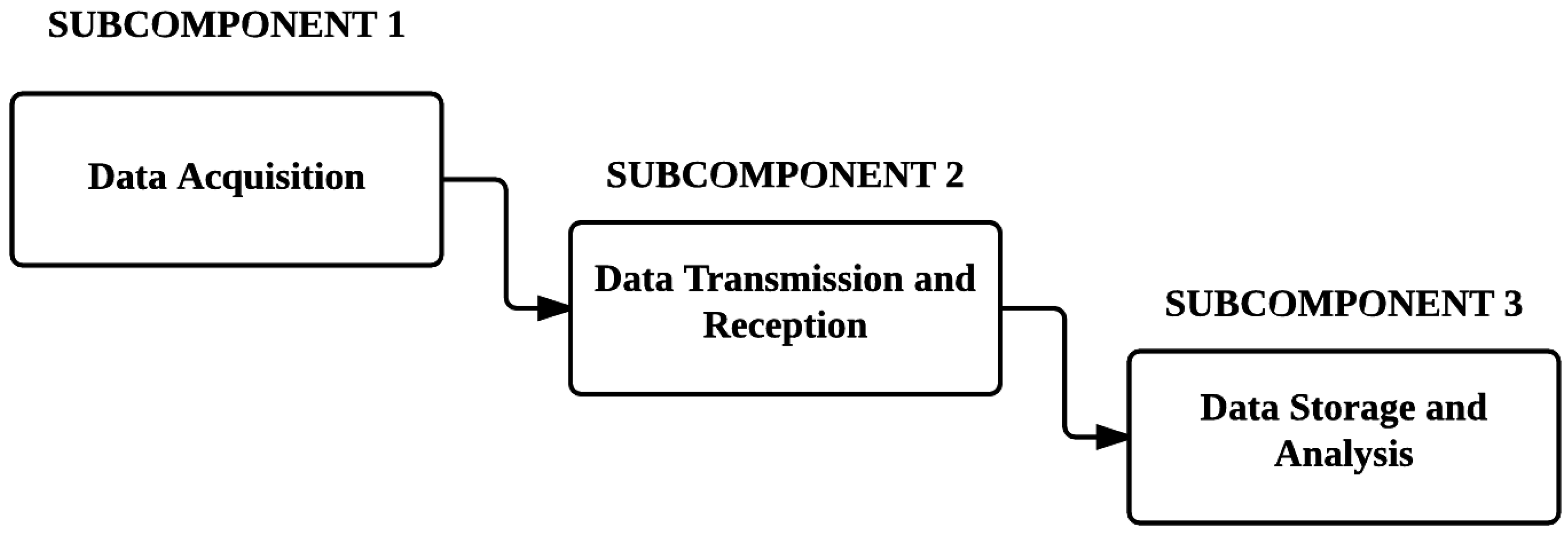
4.1. Main System Design
The main system consisted of three independent modules that is controlled by a microcontroller. The three modules included a GPS module, a GSM module, and an RFID reader module. Each module required an independent communication platform in order to provide the required data. It is, therefore, decided to make use of a 16-bit microcontroller with enough serial communication peripherals. The PIC24FJ64GB202 microcontroller is used as the main control unit of the system. Each module is interfaced to the microcontroller and the controller itself is given full control of the operation of each module.
(1) RFID reader module: The RFID reader module is an off-the-shelf product. In order to achieve a significant read range, attention should be given to both the reader and transponder antennas. It is, therefore, decided to make use of a reader that allowed for the interfacing of an external antenna (to improve the reading range of passive RFID transponder and improve accuracy of our systems [
19,
20], an external antenna is provided with the reader). The specifications of the RFID reader module, obtained from the technical documentation, can be viewed in
Table 1 below.
It is required to calculate the voltage that developed across the antenna, as well as the current that flowed through the antenna. This is done with the following two equations, which is also obtained from the technical documentation [
21].
where
is the peak-to-peak voltage across the reader antenna,
is the operating frequency of the reader,
is the value of the tuning capacitor of the reader,
is the current flowing through the antenna, and
is the value of the internal resistance of the antenna, as well as any external resistance added in series with the antenna. The module already contains an internal resistance of 22 Ω, and an internal tuning capacitance of 532 pF. It is decided to add an additional tuning capacitor with a value of 100 pF. This would give a total value of 632 pF for the tuning capacitance. The inductance of the reader antenna is measured to be approximately 2.7 mH, and the antenna also had an internal resistance of approximately 9 Ω. By using the inductance of the reader antenna and the tuning capacitance, the frequency of operation is determined with the use of Equation (3) below:
where
is the inductance of the reader antenna and
is the total tuning capacitance.
From Equation (1), the voltage is then calculated as follows:
The voltage calculated above is reduced to the maximum value stated in the module specifications. By using Equation (1), it is determined that an external resistor with a value of 100 Ω should be added, in order to adjust the voltage to a value that is within the required specifications. The total series resistance is therefore 131 Ω. From Equation (2), the current is then calculated:
The current value is well below the maximum rating specified in the specifications.
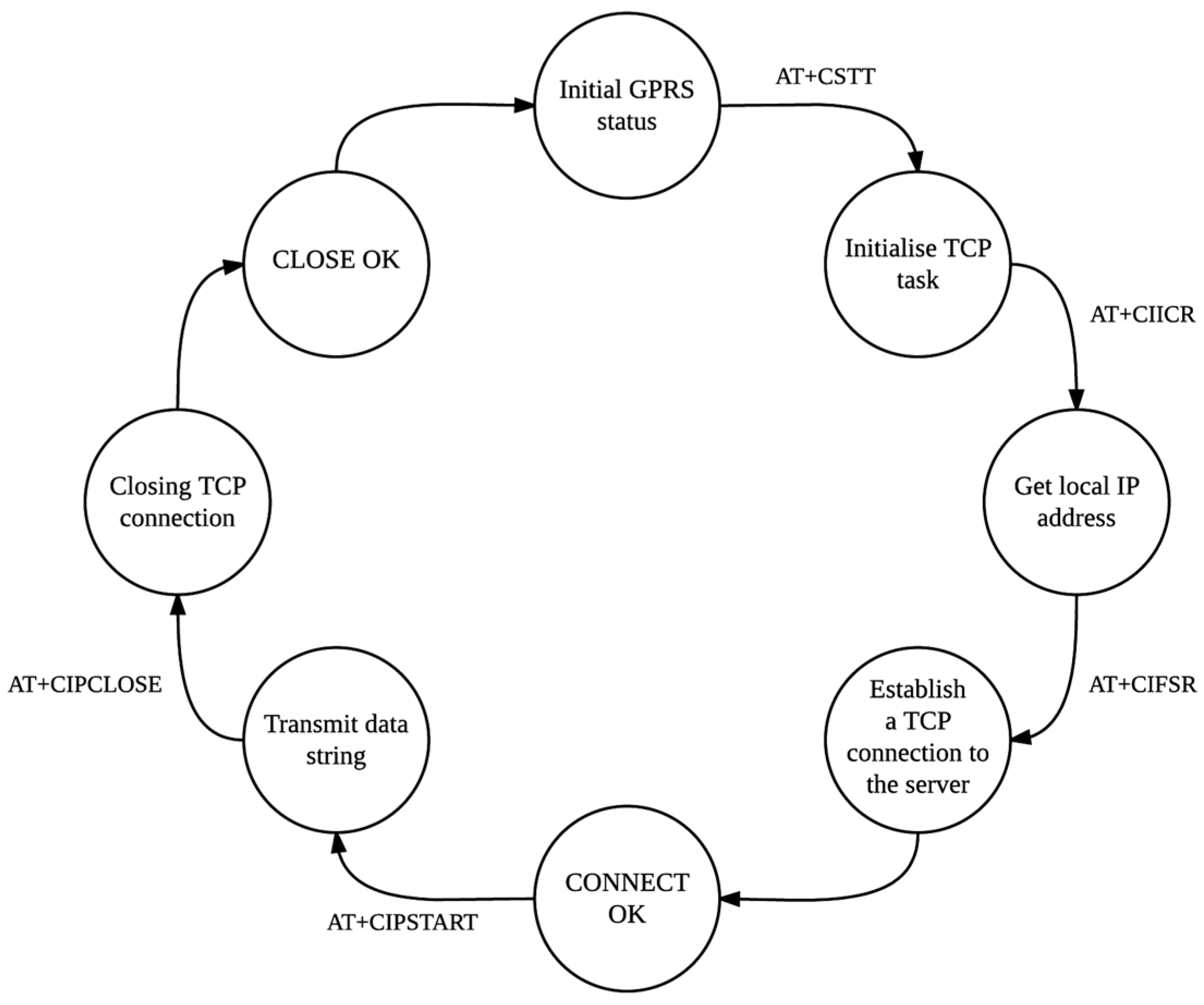
(2) GPS and GSM module: The GPS module contained an integrated GSM module as well. This allowed for the use of only one serial communication channel between the control unit and the module. Through this channel, both GPS and GSM functionalities could be accessed. Attention (AT) commands are used to facilitate communication with the module. The module itself required a separate supply voltage of 4 V and as mentioned above, a separate LiPo battery is incorporated to provide the necessary power. The module contains two receiver antennas: one antenna serves the purpose of receiving GPS signals, and the other antenna allows for an uplink to the GSM network. MTN South Africa is considered to be the service provider of choice.
Table 2 below gives an overview of the AT commands that are used in software for general module communication. All AT commands are stored on the microcontroller and this therefore allowed the control unit to have full control over the module.
The state machine in
Figure 2 above has been implemented on the control unit and is executed regardless of whether the system is in RFID mode or GPS mode. The only difference between the RFID mode and the GPS mode with regards to the wireless transmission of data, is the data string itself (in RFID mode, a tag ID is presented and not GPS data).
(3) Database system and Graphical User Interface: The database system is implemented with the use of the PHP scripting language. As mentioned above, all data strings are in the form of a POST command. The server received the transmitted strings via the established TCP connection and updated the database fields with the retrieved information. The transmitted data consisted of a vehicle registration number, the longitude coordinates, the latitude coordinates, the longitude indicator (North or South), the latitude indicator (East or West), and a timestamp. For the RFID transponder, the data string consisted of only a vehicle registration number, a transponder ID, and a timestamp. The transponder ID is considered to be linked to a specific GPS coordinate set, which is also stored in the database. The purpose of the GUI is to retrieve the stored data in the database to determine and plot a route by use of use of a Google Maps interface.
A Kalman filter is incorporated into the design of the interface in order to offer the application some level of prediction. The filter is only considered as a tool in the broader picture of the vehicle estimation algorithm. The Accord.NET math library is also used to assist with this task.
4.2. RFID Transponder Design
The main objective is to design and implement the RF front-end of the RFID transponder. This consists of the design and implementation of an LC tank that resonates on the carrier frequency of the RFID reader module. The resonant frequency is once again determined by Equation (3). Extensive simulations have been conducted on different antenna sizes and parameters. The purpose of the simulations is to obtain a relationship between the different antenna parameters and the induced voltage, measured at different load values. The internal parameters that are present in the LC tank are listed in
Table 3 [
22].
The coil inductance and coil capacitance is considered to be the two crucial parameters, due to the fact that these parameters directly affect the frequency of operation of the transponder, based on Equation (1). The internal capacitance of the coil is not enough to allow for resonance at the frequency of operation. It is, therefore, required to add additional capacitance to the coil. This additional capacitance, together with the inherent capacitance of the coil and the parasitic capacitance present in the internal circuitry of the transponder, forms an LC tank.
It is found that an increase in the antenna diameter, as well as an increase in the number of windings of the antenna, leads to an increase in the induced voltage across the antenna coil.
- 1)
Antenna simulations and hardware design: They are two options for the best practical implementation of the transponder. The first design choice is to make use of a circular shaped antenna, due to the fact that most off-the-shelf passive tags today has an internal circular coil. The equation for the inductance of an N-turn multilayer circular coil is as follows [
22]:
where L is the inductance of the coil in μH, a is the average radius of the coil in centimeters, N is the number of windings of the coil, h is the height of the coil windings in cm, and b is the thickness of the coil windings in cm.
Table 4 shows the design parameters of the circular coil.
The antenna parameters in the table above are chosen such that a high quality factor can be obtained. By keeping the internal resistance as low as possible, a high quality factor can be obtained, as is discussed in the theoretical background section. The inductance of the coil can now be calculated with the use of Equation (4):
Using Thompson’s Equation (3), the capacitance can be calculated which would allow for resonance to be achieved on the desired frequency of 129 kHz.
After the calculation of the required capacitance, the next step is to determine the theoretical internal resistance of the coil. As discussed in the theoretical background section, two types of resistances are present: a DC resistance value and an AC resistance value. The DC resistance for the circular loop antenna will now be calculated:
In order to calculate the AC resistance of the coil, the skin depth for copper wire at a frequency of 129 kHz should first be calculated:
The AC resistance of the coil can now be calculated from the approximated AC resistance equation:
The total amount of ohmic losses is the sum of the values of the DC resistance and AC resistance of the coil. It should be noted that the internal radiation resistance of the coil can be considered as negligible.
With the total theoretical internal resistance calculated, the quality factor (Q-factor) of the coil can now be determined:
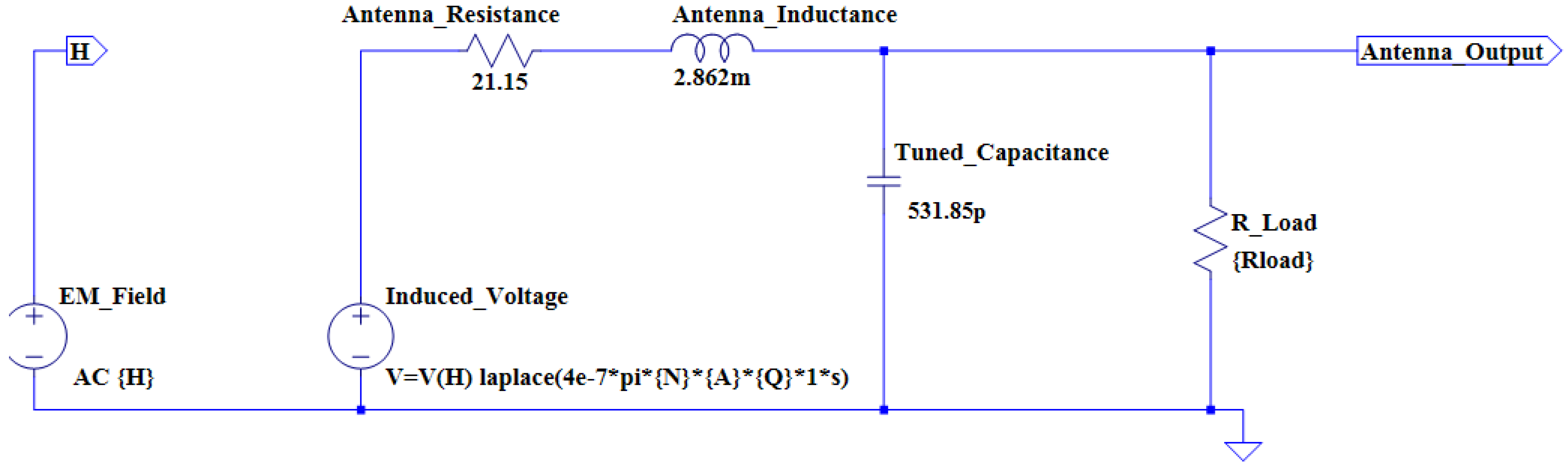
From the calculations above, it is possible to construct an antenna model using the LTSpice IV simulation software.
Figure 3 illustrates the antenna model for the circular coil antenna.
The second antenna design option is use of a square shaped antenna. The mathematical calculations for the antenna parameters are considered to be more complex. A different shape is considered in order to determine and compare the performance of two geometrically different coils. Furthermore, it is also decided to increase the geometrical dimensions of the square loop coil. It is decided to reduce the theoretical inductance value of the second coil to 1 mH, in order to determine whether a relationship exists between two different inductance values. The equation for the inductance of an N-turn multilayer square coil is as follows [
22]:
where N is the number of windings, a is the distance between the center of the square coil and the outer edge of the coil windings, b is the width of the coil winding, and c is the height of the coil winding.
Table 5 shows the design parameters for the square loop antenna.
Using Equation (5), and assuming an inductance value of 1 mH, the number of windings for the square coil can be calculated:
Using Equation (3), the capacitance can again be calculated that would allow a resonance to be achieved at a frequency of 129 kHz. Since the inductance is chosen to be 1 mH, the tuning capacitance should be recalculated:
The next step is to determine the theoretical internal resistance of the coil. Both the DC resistance and AC resistance needs to be recalculated for the square antenna due to the fact that the geometric parameters differ from that of the circular coil:
The AC resistance of the coil can be calculated from the approximated AC resistance equation. It should be noted that the skin depth stays constant for both antennas, since both antennas will be constructed from copper wire and both will operate at a frequency of approximately 129 kHz:
The total amount of ohmic losses are as follows:
With the total theoretical internal resistance calculated, the quality factor (Q-factor) of the coil can now be determined.
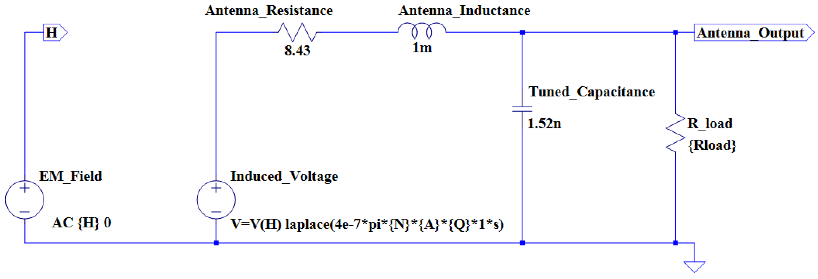
An antenna model is once again constructed in LTSpice IV.
Figure 4 illustrates the antenna model for the square coil.
- 2)
Transponder power supply circuitry: The designed LC tank provides two important abilities to the RFID transponder. The first ability is that the transponder can draw the required power for effective operation from the RF-field. As mentioned above, this power is made available by the RFID reader module. The second ability is that the transponder can effectively communicate with the RFID reader [
23] module through the RF-field. This allows for the transfer of the transponder ID to the reader module.
The next step in the design process is to design, simulate and implement a power supply system for the transponder. The power supply system receives an AC power signal from the LC tank. This signal should be converted into a stable DC power signal in order to power the internal circuitry of the transponder. It is decided to implement a full-wave bridge rectifier for the rectification stage of the power supply. The full-wave bridge rectifier allows for the passage of current in one direction only during a full AC cycle. During the positive half cycle, diodes D1 and D3 is forward biased and diodes D2 and D4 is reversed biased. For the negative half-cycle, D1 and D3 is reverse biased and D2 and D4 is forward biased. In order to achieve a maximum interrogation range, the power consumption of the transponder should be as low as possible. It is, therefore, decided to make use of Schottky diodes due to the fact that they have a minimal forward voltage drop (a forward voltage drop of approximately 0.2 V is measured during the implementation phase of the transponder).
Figure 5 shows the simulation model of the LC tank and rectifier circuit:
The next phase is to filter and smooth the rectified signal in order to provide a clean and stable DC supply to the rest of the transponder electronics. This is done with the addition of filter capacitors after the rectification stage. Equation (6) can be used to calculate the value of the filter capacitors [
24]:
where
is the ripple voltage,
is the maximum input voltage,
is the frequency of the input signal,
is the load value, and C is the filter capacitor value.
Since the frequency of the input voltage is between 125 kHz and 134 kHz, the overall ripple voltage will remain significantly small. Since a microcontroller is used for the software part of the transponder, the filter capacitance value is chosen to be relatively high, in order to reduce the external effects that a high internal oscillator might have on the system. Three separate capacitors are incorporated into the design: a 470 µF electrolytic capacitor, a 22 µF electrolytic capacitor and a 100 nF ceramic capacitor. If it is assumed that the maximum input voltage is 20 V, the ripple voltage for a 50 kΩ load can be calculated as follows:
The final design phase in the transponder power supply unit is to design and implement a voltage regulator circuit in order to limit the supply voltage of the transponder to the desired operating voltage of the internal circuitry. If the distance between the transponder and reader is decreased, the coupling coefficient is increased, which leads to a dramatic increase in the induced voltage over the transponder antenna. In order to limit the supply voltage, the approach described in [
15] is followed, which involved the design of a shunt regulator circuit with the use of a transistor and Zener diode. Equation (7) shows how the value of the shunt resistor can be calculated [
15], if the value of the load, as well as the coupling coefficient is known:
where k is the coupling coefficient between the reader and transponder,
is the inductance of the reader antenna,
is the inductance of the transponder antenna,
is the current flowing through the reader antenna,
is the internal resistance of the transponder coil,
is the capacitance value of the tuning capacitor, and
is the load resistance [
15]. Typical resistance values of the shunt regulator are in the order of a few hundred ohms to one kilo ohm [
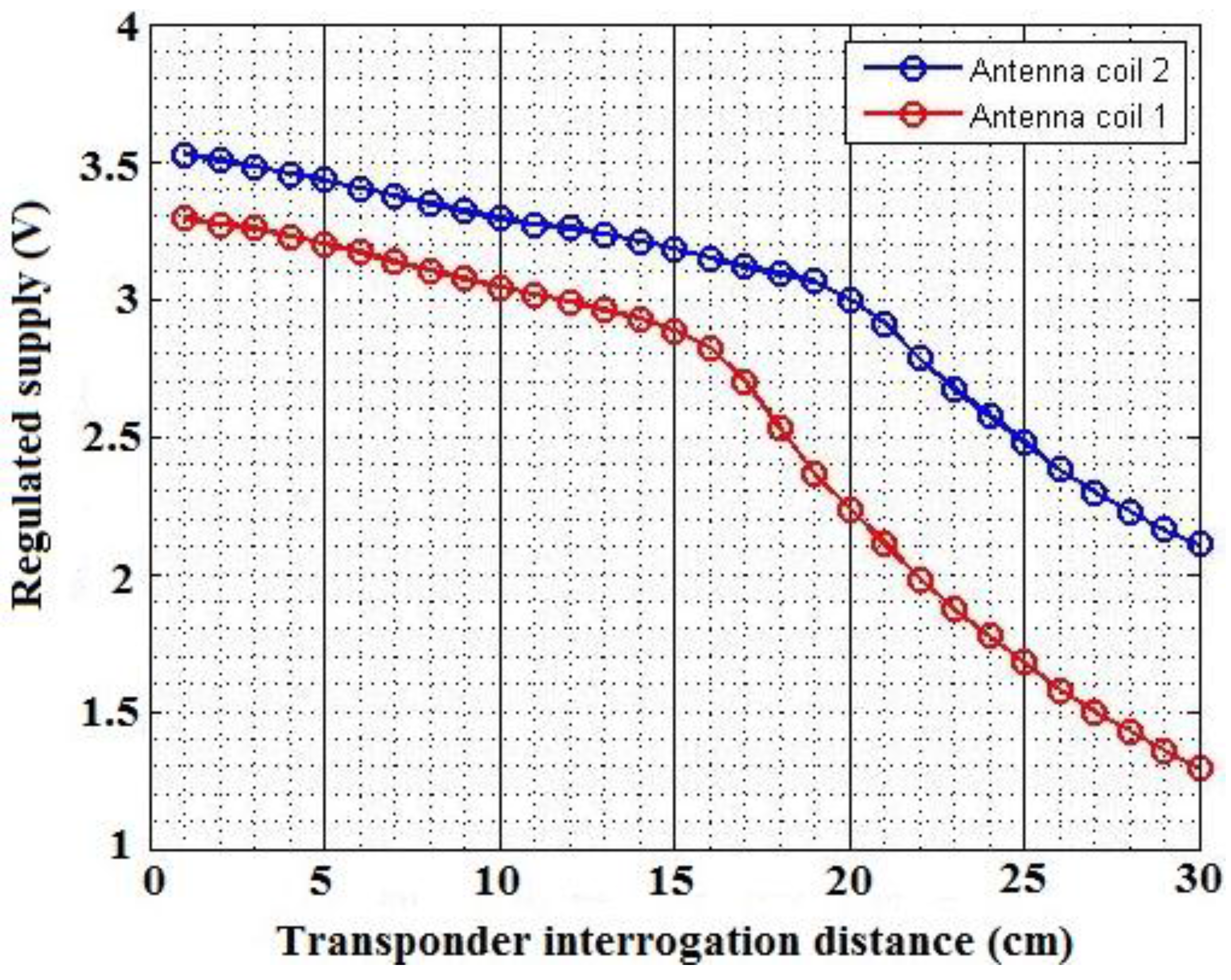
15]. Since the voltage would be very low at a reading distance of 25 cm to 30 cm, the use of a perfect shunt regulator is not really required. It is, however, still implemented in order to provide protection at smaller distances. Once the Zener breakdown voltage has been reached, the Zener will start to conduct and the base of the transistor will switch on. Current will then flow through the regulator circuit, which limits the voltage.
- 3)
Transponder load modulation circuitry: The next phase in the design process is to design, simulate, and implement the load modulation circuit. The purpose of the load modulation circuit is to manipulate the RF-field between the reader and transponder, in order to transmit data from the transponder to the reader. The load modulator consists of a resistor and a switch. The resistor is directly connected to the LC tank. The purpose of the switch is to connect or disconnect the resistor to or from the antenna. By doing so, the parameters of the transponder resonant circuit are changed, which results in variations in the magnitude and phase of the transponder impedance (modulation). The variations can be detected by the reader through the RF-field, and by applying an appropriate procedure, the reader can reconstruct (demodulate) the transmitted data. The switch is implemented with the use of a FET, due to the fact that FETs are used in the construction and fabrication of logic switches in the field of microelectronics. A PIC microcontroller is used as the data carrier, and the transmission pin of the data carrier is directly connected to the gate of the FET. This allows the data carrier to have full control over the modulation. The source of the FET is connected to the resistor which, in turn, is connected to one of the resonant circuit terminals.
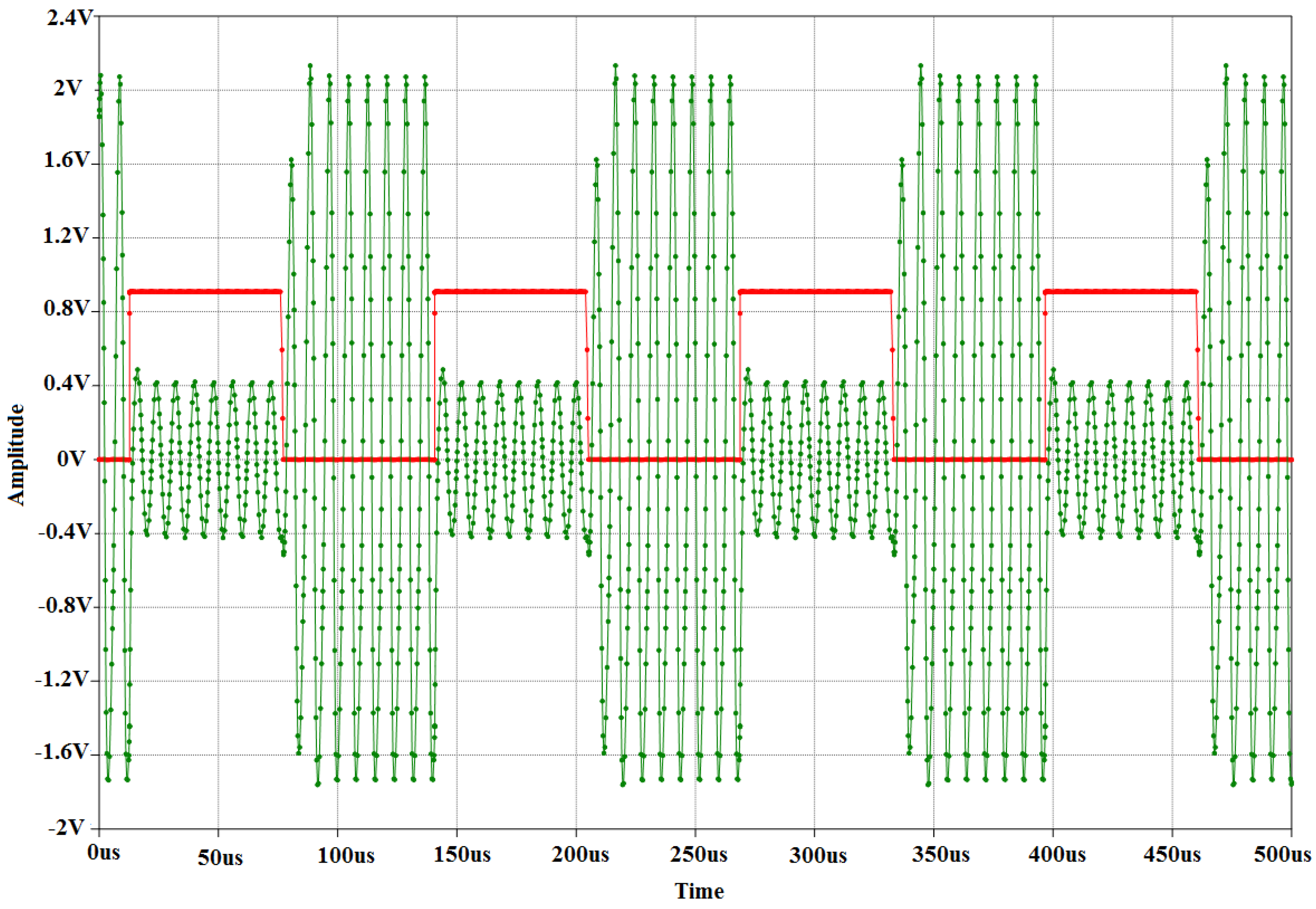
Figure 6 shows the simulation model for the load modulator. A simple clock divider circuit is implemented in order to simplify the simulation of load modulation. The purpose of the clock divider is to simulate the real-time transmission of data from the microcontroller. The EM4100 RFID communication protocol has been implemented on the transponder. This implies that data bits are transmitted at a rate of 2 kHz. In the simulation, a sine wave generator is used to simulate the induced voltage in the resonant circuit. The resonant circuit is represented by an inductor and capacitor. The load modulator is connected to the resonant circuit and receives a square wave input from the clock divider.
Figure 6 shows the transient analysis of the load modulator simulation.
- 4)
Transponder data carrier: The transponder resonant circuit, load modulator, and power supply unit have been designed and implemented in hardware, as discussed above. The hardware components allow for the harnessing of power and the transmission of data. Next, in the transponder design is to implement the data carrier. The data carrier serves the purpose of transmitting the digital ID of the transponder. An ID, consisting of 10 hexadecimal values for compliance to the EM4100 RFID communication protocol, is chosen and converted to the corresponding binary values. A software routine is implemented on the microcontroller to transmit the corresponding bit values. Transmission is done by controlling the voltage of one of the microcontroller pins (a high pin voltage corresponds to the transmission of a binary one and a low pin voltage corresponds to a binary zero). The main constraint in the transponder design is the amount of power available. It is, therefore, decided to use a low-power microcontroller for the data carrier.
The design consists of the transmission of nine header bits. The header bits are all logical high bits. The second phase consists of the transmission of the actual data bits. A total of 10 hexadecimal values are transmitted, which equates to a total of 40 bits. The EM4100 protocol makes use of even parity for data validation purposes. In addition to the 40 data bits, each hexadecimal value receives a parity bit, which results in a total of 5 bits per hexadecimal value. With the parity bits included in the transmission, the total number of data bits is 50. The last phase is to transmit a column parity bit combination, as well as the stop bit. The column parity combination consists of 4 parity bits. The total number of bits that are transmitted is therefore 64. The transmission of data will be repeated as long as the transponder has sufficient power to operate.
The data bits cannot be directly transmitted. It is required to first encode the transmission bits before activating the load modulator. The general line encoding scheme that is used in low-frequency RFID transponders is Manchester encoding. Manchester encoding can be implemented as hardware architecture, or as a software routine. The hardware implementation requires the use of an XOR gate. The transmission rate clock and the data itself serves as inputs to the gate and the resulting output, which is the Manchester encoded data, is connected to the gate of the load modulator switch. Two software routines are implemented, one routine for a logical high and another routine for a logical low. The data is directly encoded in software which implies that the output pin of the microcontroller can directly be connected to the load modulator. The two routines consisted of a logical high or low value, followed by a delay routine. The EM4100 requires a transmission rate of 2 kHz (64 carrier frequency clock cycles) or 4 kHz (32 carrier frequency clock cycles) when a carrier frequency of 125 kHz is used. A transmission rate of 64 clock cycles is chosen, which implies that a delay of 32 clock cycles would be required to encode the data with the Manchester encoding scheme. Since the RFID reader module is configured to operate at a carrier frequency of 129 kHz, the time delay required for the Manchester encoding scheme can be calculated from Equation (8):
If a binary one needs to be transmitted, the output pin of the microcontroller will output a binary zero for 248 microseconds and a binary one for another 248 microseconds. This results in a transmission rate of 2.015 kHz (496 μs).
Figure 7 shows the Manchester encoding subroutines that are implemented.
The software routines that are implemented on the low-power microcontroller required an accurate clock rate in order to execute optimally. A 4 MHz internal oscillator is used to ensure that the delays could be accurately calculated. It is found that, although the microcontroller can operate at low voltages, the clock speed of the microcontroller is not operating at the speed required to produce an accurate delay. This implies that although the microcontroller is activated at low voltage levels, communication between the reader and transponder would not succeed due to an inaccurate transmission rate.
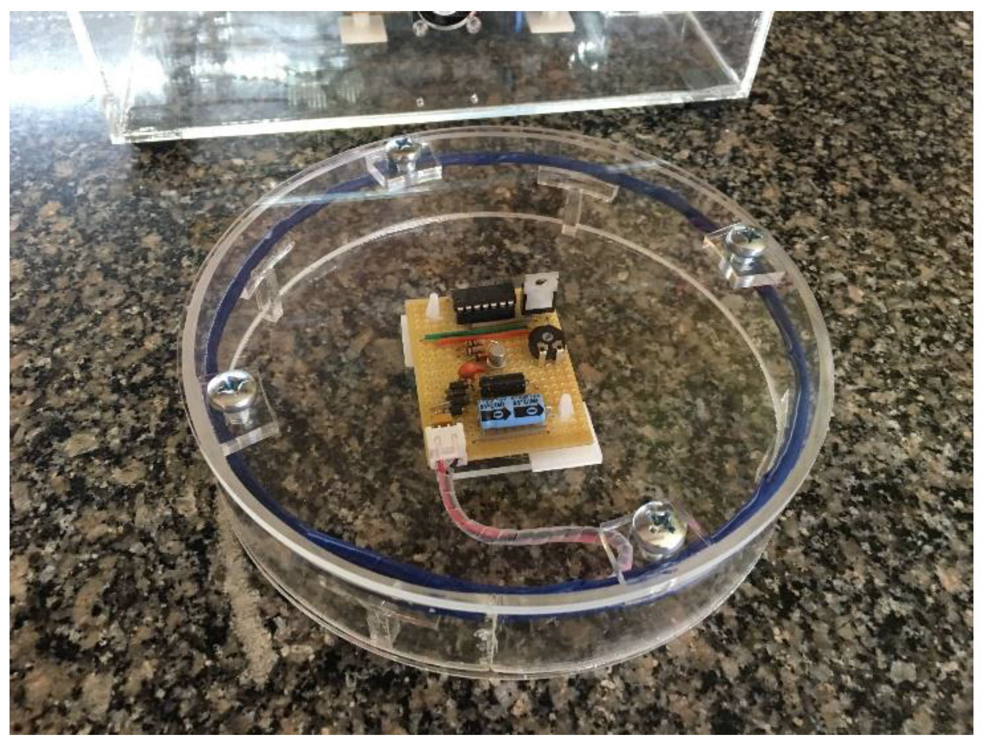
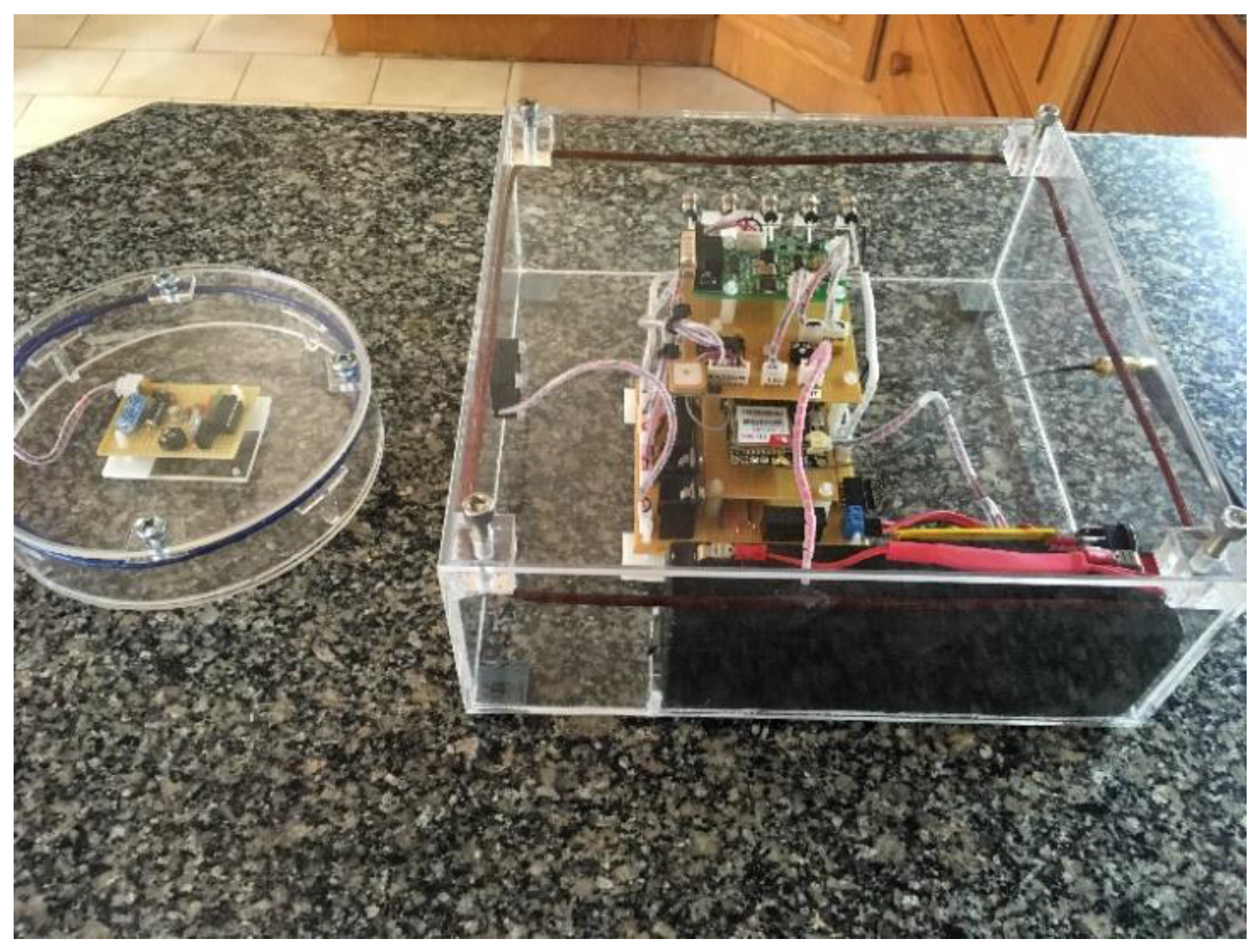
Figure 8 and
Figure 9 show the main system, as well as the RFID transponder with the circular coil.


