
Photon-Counting Arrays for Time-Resolved Imaging

 , , and
Abstract
:
1. Introduction
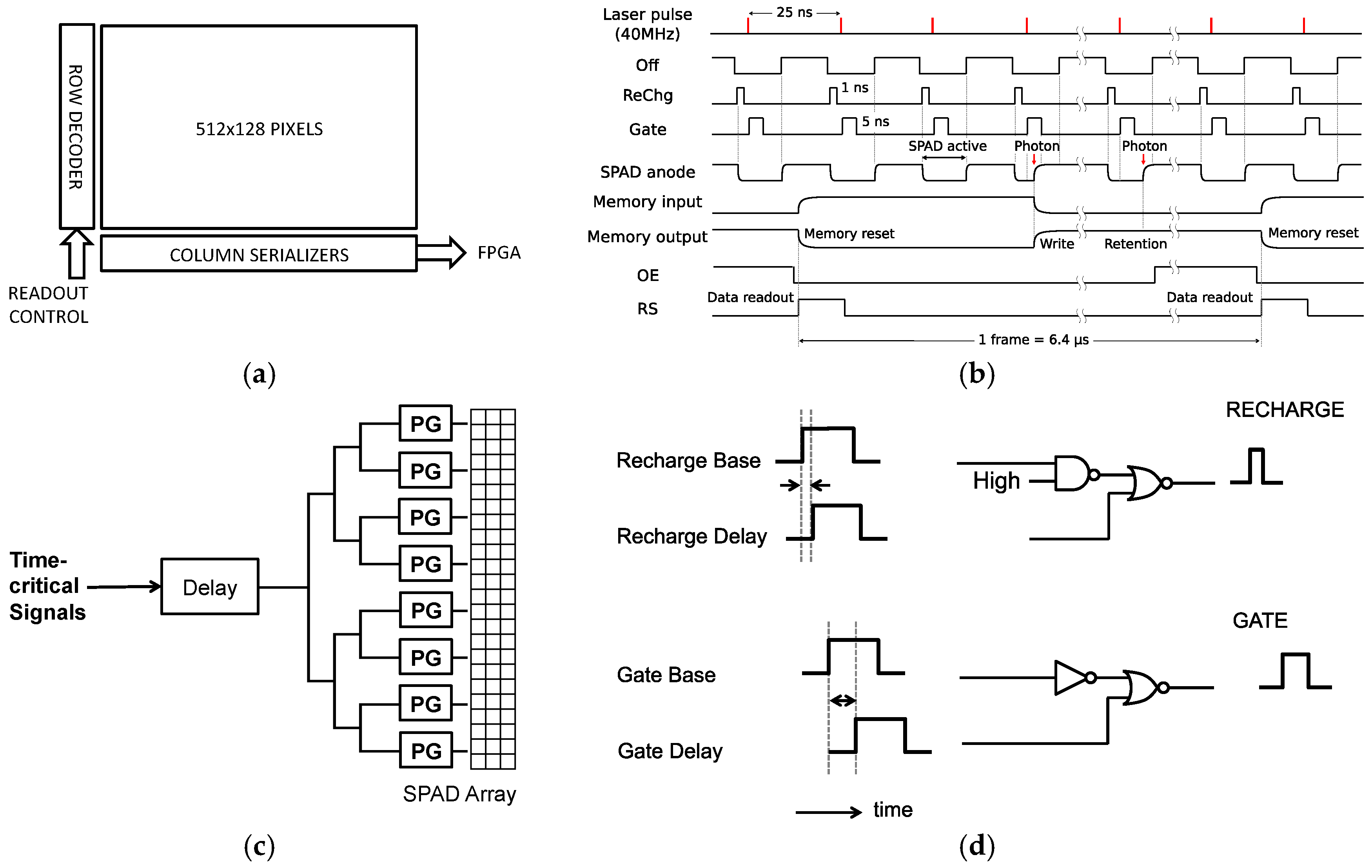
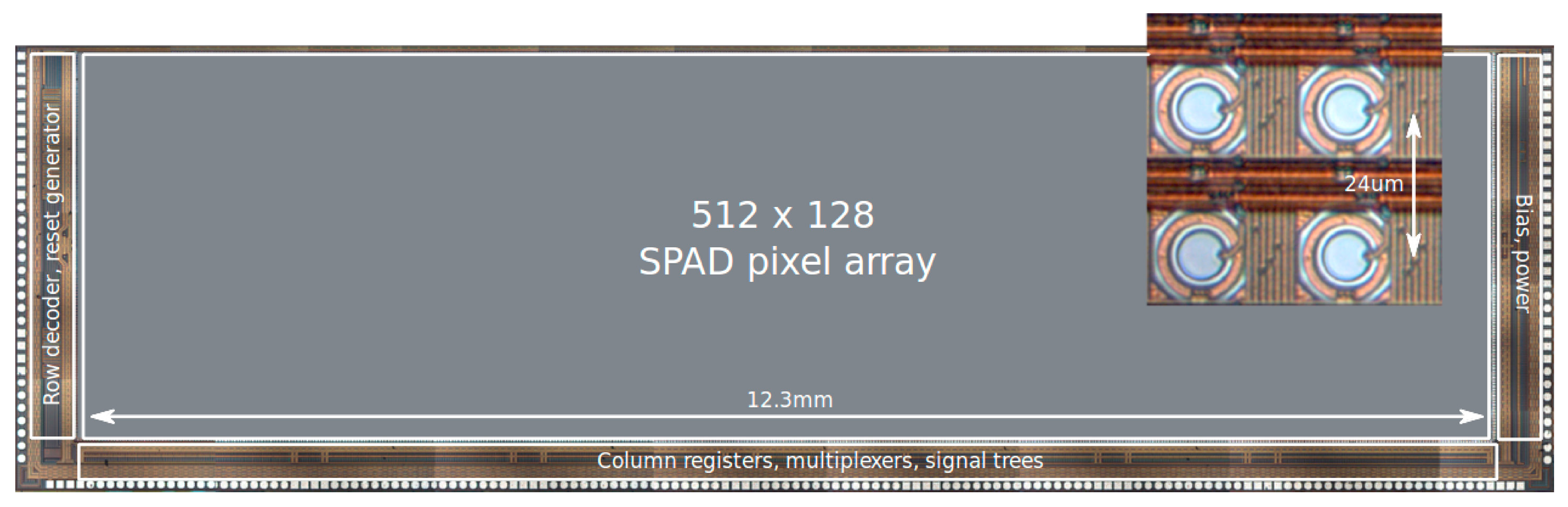
2. Sensor Architecture
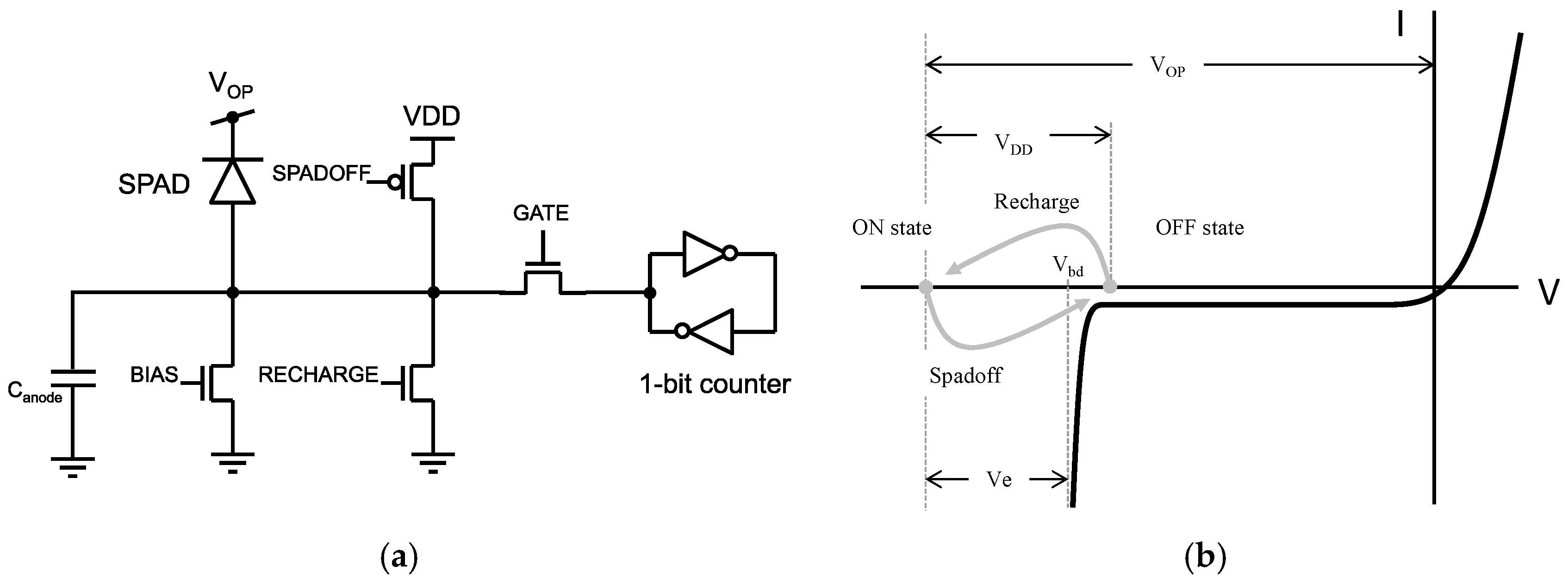
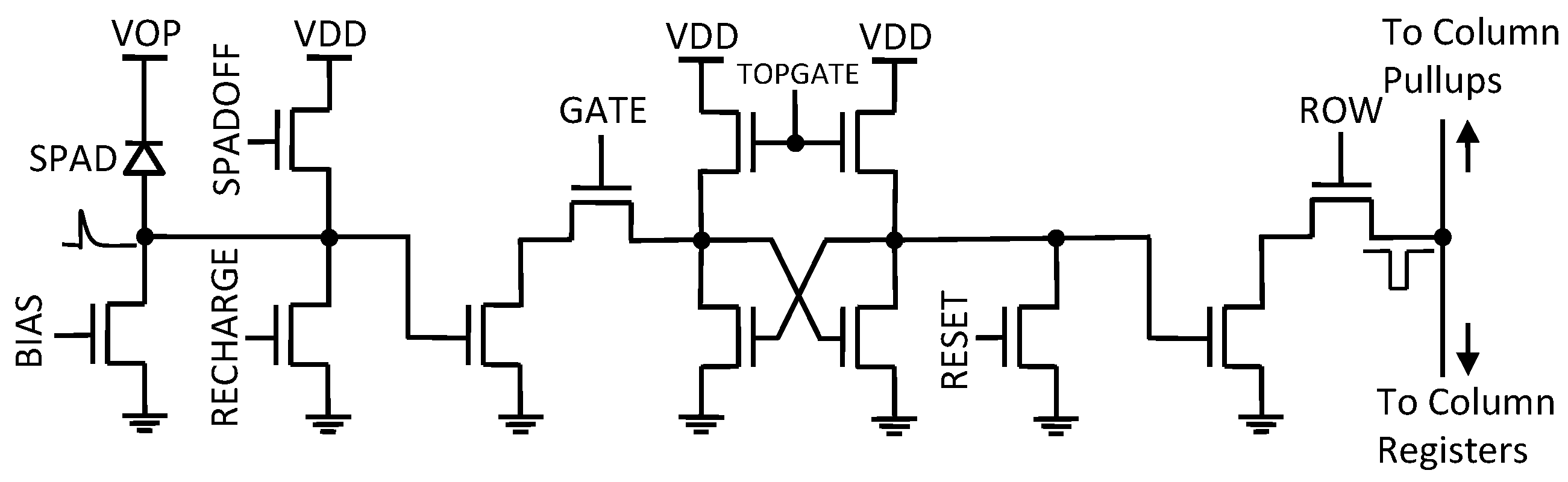
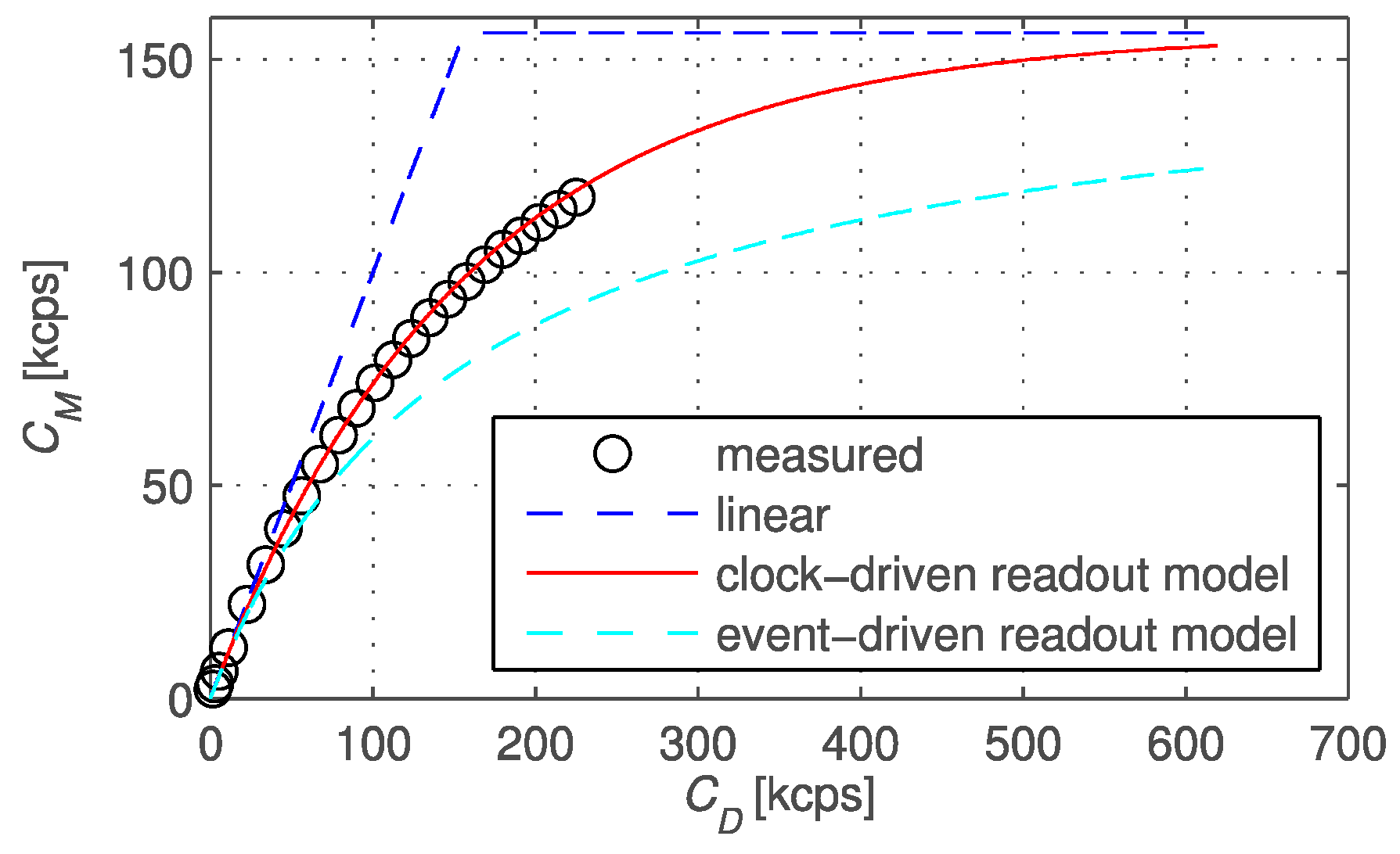
3. Binary Pixels
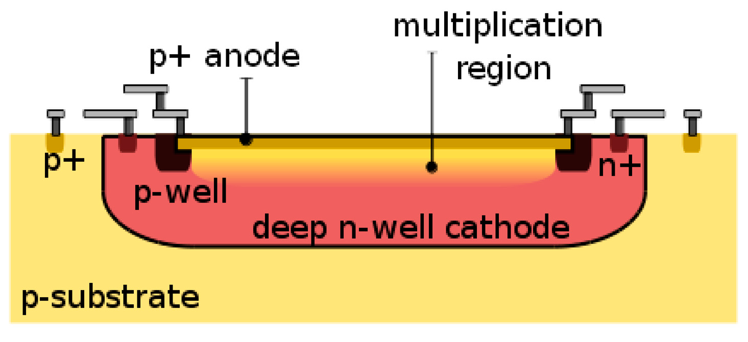
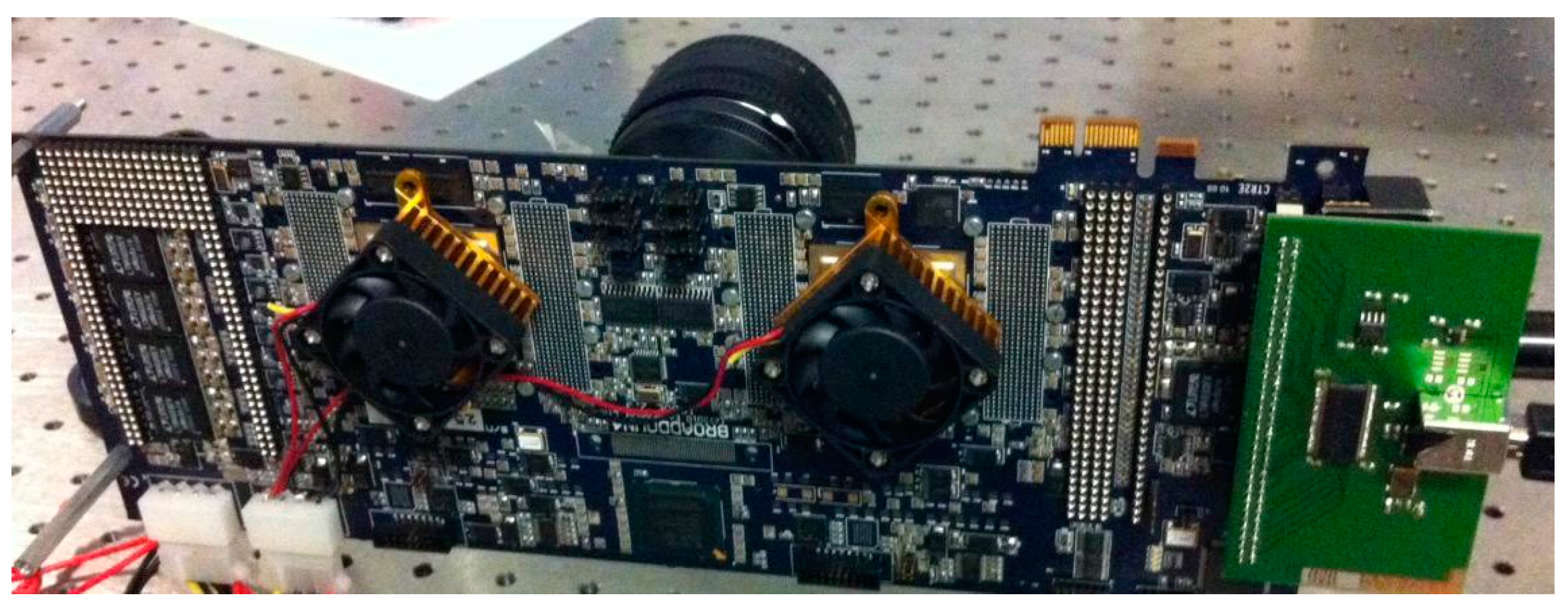
4. Sensor Fabrication
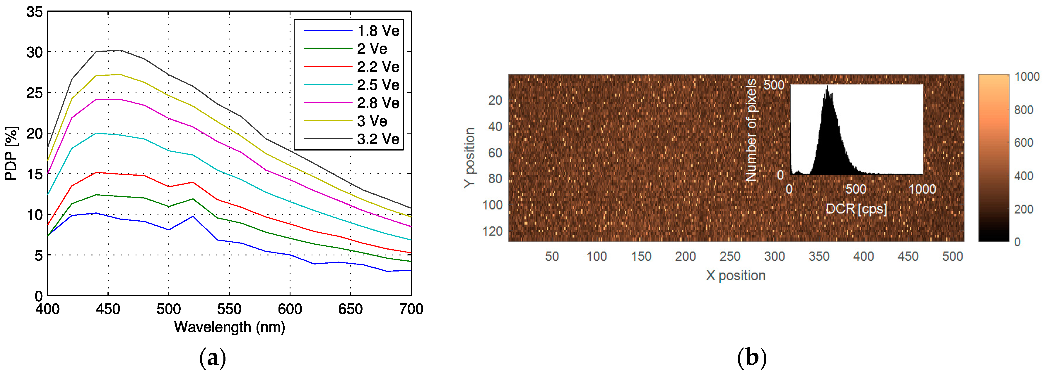
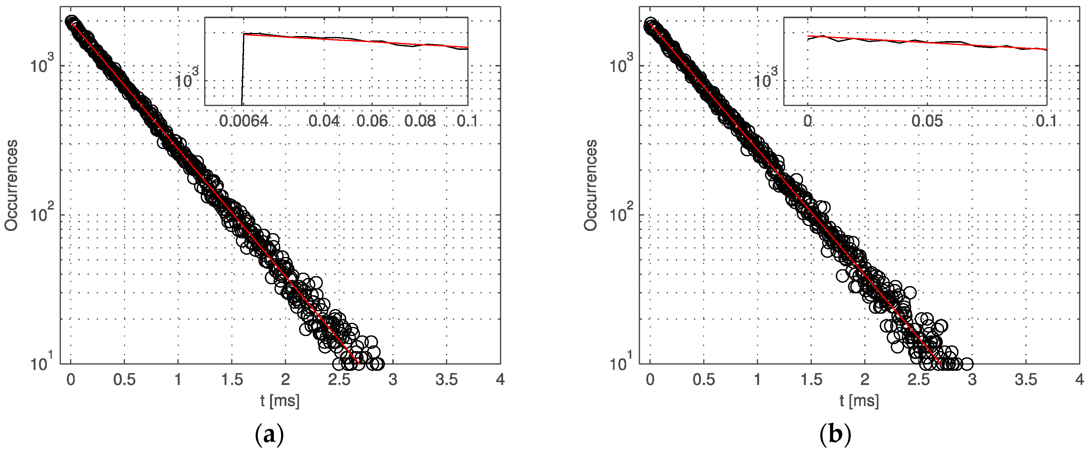
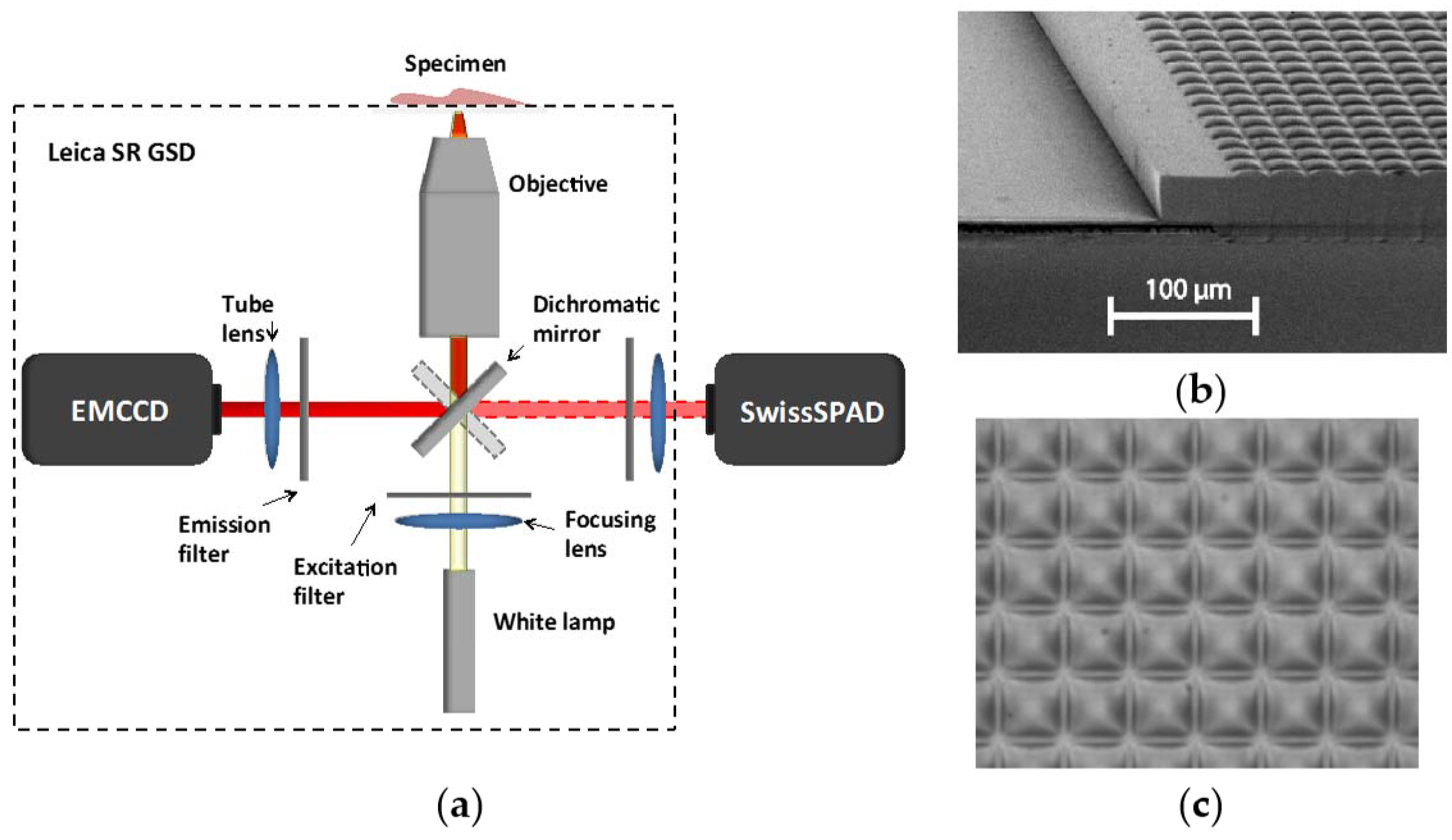
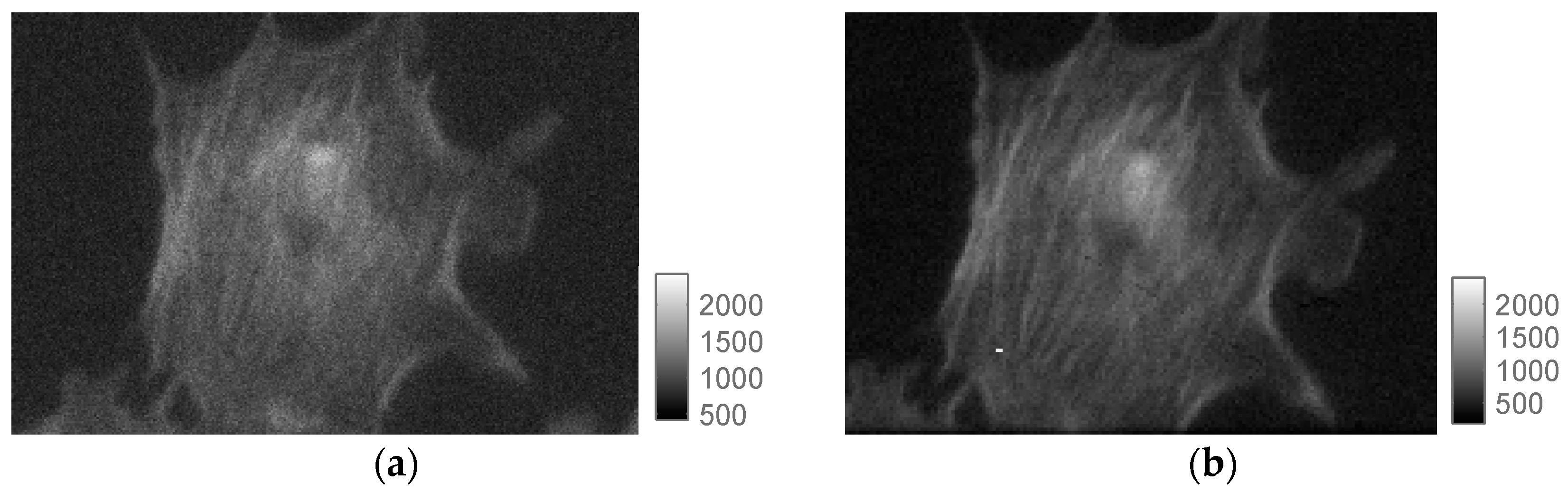
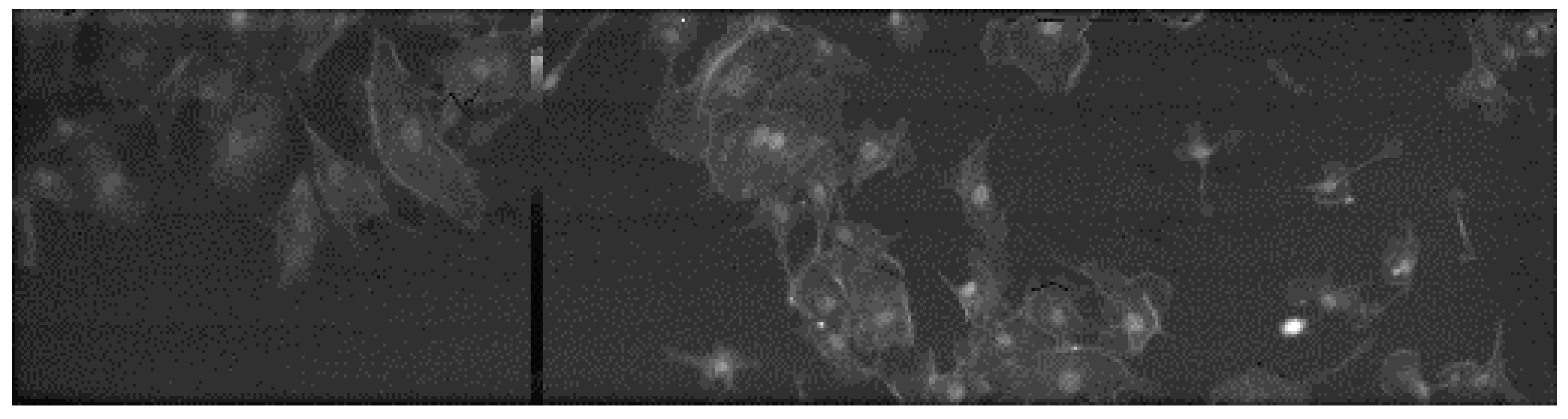
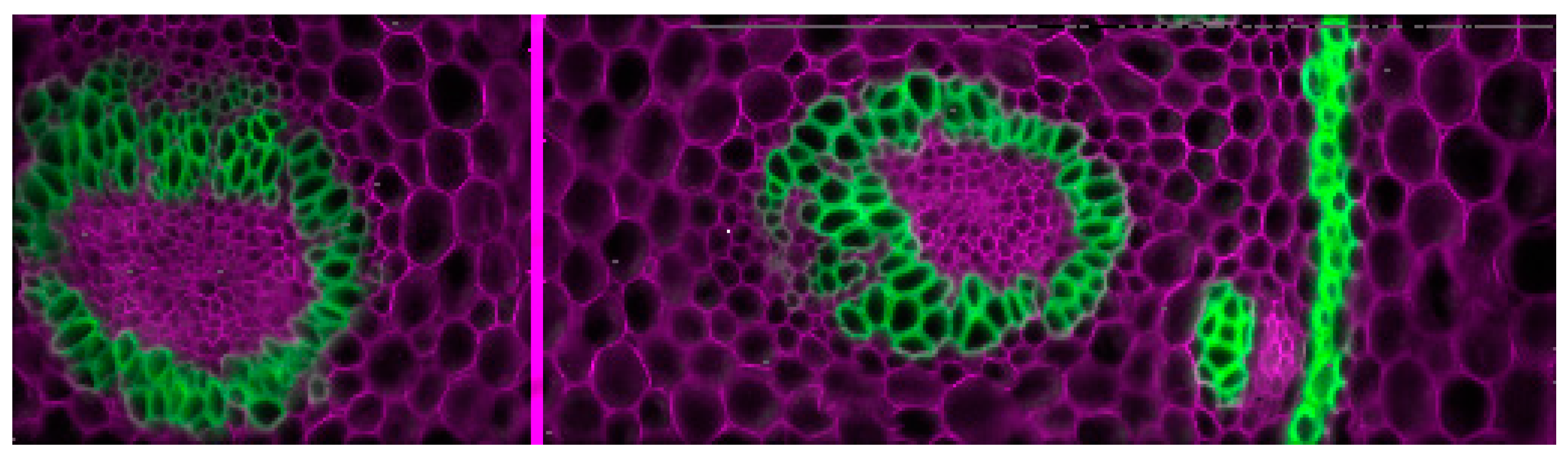
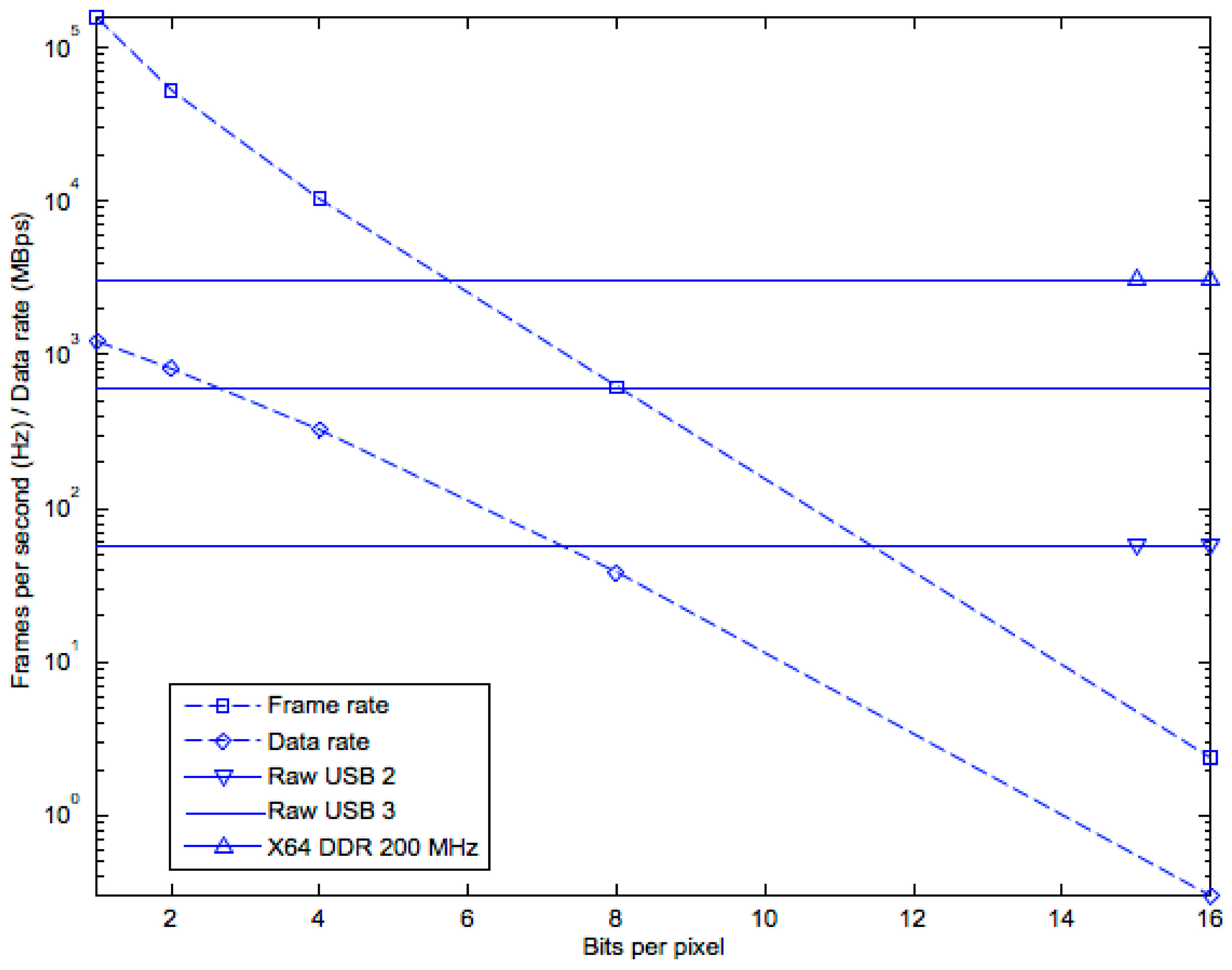
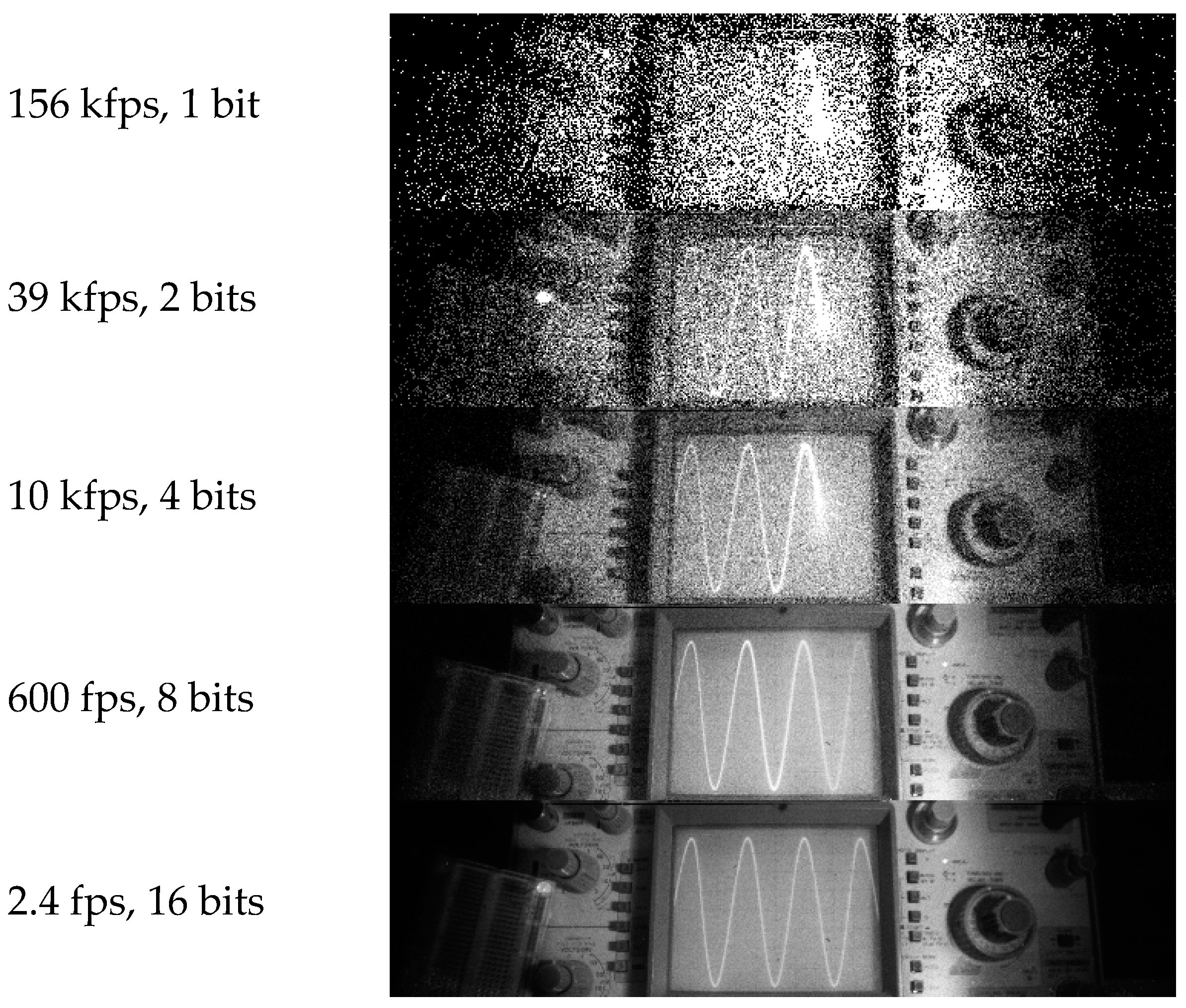
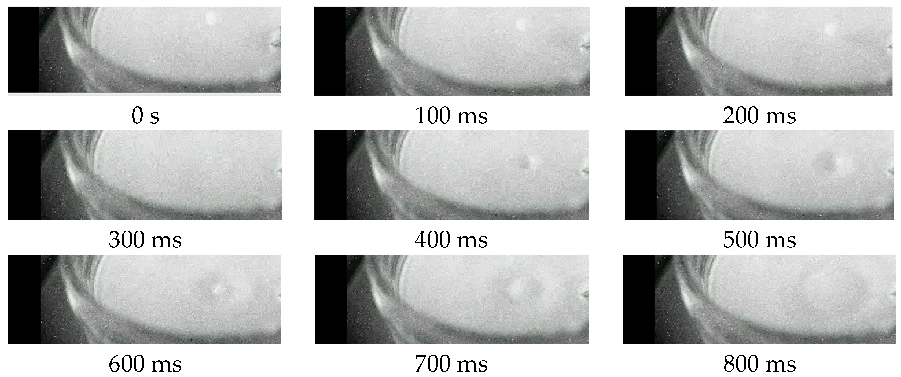
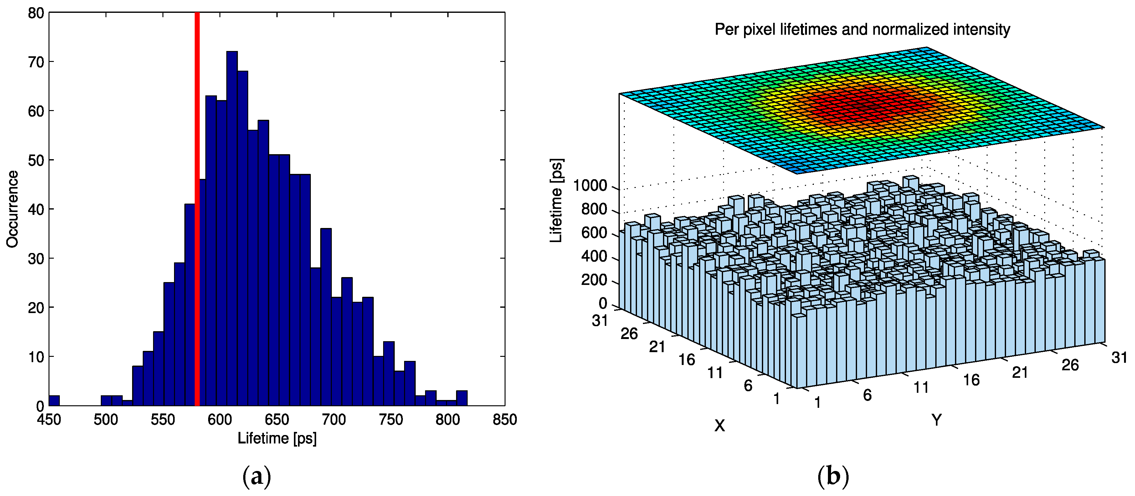
5. Results
6. Conclusions
Supplementary Materials
Acknowledgments
Author Contributions
Conflicts of Interest
Abbreviations
| SPAD | Single-photon avalanche diode |
| FLIM | Fluorescence lifetime imaging microscopy |
| EMCCD | Electromultiplied charge-coupled device |
| SNR | Signal-to-noise ratio |
| PRNU | Photo-response non-uniformity |
| DCR | Dark count rate |
| PDP | Photon detection probability |
| PDE | Photon detection efficiency |
| BPAE | Bovine pulmonary artery endothelial cells |
| DAPI | 4′,6-Diamidino-2-phenylindole |
| IRF | Instrumentation response function |
| TCSPC | Time-correlated single photon counting |
| ENOB | Effective number of bits |
| ICG | Indocyanine green |
References
- Ghioni, M.; Gulinatti, A.; Rech, I.; Zappa, F.; Cova, S. Progress in silicon single-photon avalanche diodes. IEEE J. Sel. Top. Quantum Electron. 2007, 13, 852–862. [Google Scholar] [CrossRef]
- Rochas, A.; Gosch, M.; Serov, A.; Besse, P.A.; Popovic, R.S.; Lasser, T.; Rigler, R. First fully integrated 2-D array of single-photon detectors in standard CMOS technology. IEEE Photon. Technol. Lett. 2003, 15, 963–965. [Google Scholar] [CrossRef]
- Niclass, C.; Sergio, M.; Charbon, E. A single photon avalanche diode array fabricated in 0.35-μm CMOS and based on an event-driven readout for TCSPC experiments. Proc. SPIE 2006, 6372, 63720S. [Google Scholar]
- Webster, E.A.G.; Richardson, J.A.; Grant, L.A.; Renshaw, D.; Henderson, R.K. A single-photon avalanche diode in 90-nm CMOS Imaging technology with 44% photon detection efficiency at 690 nm. IEEE Electron Device Lett. 2012, 33, 694–696. [Google Scholar] [CrossRef]
- Webster, E.A.G.; Grant, L.A.; Henderson, R.K. A high-performance single-photon avalanche diode in 130-nm CMOS imaging technology. IEEE Electron Device Lett. 2012, 33, 1589–1591. [Google Scholar] [CrossRef]
- Veerappan, C.; Charbon, E. A substrate isolated CMOS SPAD enabling wide spectral response and low electrical crosstalk. IEEE J. Sel. Top. Quantum Electron. 2014, 20, 3801507. [Google Scholar] [CrossRef]
- Charbon, E. Single Photon Imagers; Proc. CLEO, Sci. Innov.: San Jose, CA, USA, 2014. [Google Scholar]
- Becker, W. The bh TCSPC Handbook; Becker & Hickl: Berlin, Germany, 2014. [Google Scholar]
- Gersbach, M.; Boiko, D.L.; Niclass, C.; Petersen, C.C.H.; Charbon, E. Fast-fluorescence dynamics in nonratiometric calcium indicators. Opt. Lett. 2009, 34, 362–364. [Google Scholar] [CrossRef] [PubMed]
- Gadella, T.W.J.; Jovin, T.M.; Clegg, R.M. Fluorescence lifetime imaging microscopy (FLIM): Spatial resolution of microstructures on the nanosecond time scale. Biophys. Chem. 1993, 48, 221–239. [Google Scholar] [CrossRef]
- Gersbach, M.; Maruyama, Y.; Trimananda, R.; Fishburn, M.W.; Stoppa, D.; Richardson, J.A.; Walker, R.; Henderson, R.K.; Charbon, E. A time-resolved, low-noise single-photon image sensor fabricated in deep-submicron CMOS technology. IEEE J. Solid-State Circuits 2012, 47, 1394–1407. [Google Scholar] [CrossRef]
- Tosi, A.; Villa, F.; Bronzi, D. Low-noise CMOS SPAD arrays with in-pixel time-to-digital converters. Proc. SPIE 2014, 9114, 91140C. [Google Scholar]
- Stoppa, D.; Borghetti, F.; Richardson, J.A.; Walker, R.; Grant, L.; Henderson, R.K.; Gersbach, M.; Charbon, E. A 32 × 32-pixel array with in-pixel photon counting and arrival time measurement in the analog domain. In Proceedings of the European Solid-State Circuits Conference (ESSCIRC’09), Athens, Greece, 14–18 September 2009; pp. 204–207.
- Veerappan, C.; Richardson, J.A.; Walker, R.; Li, D.-U.; Fishburn, M.W.; Maruyama, Y.; Stoppa, D.; Borghetti, F.; Gersbach, M.; Henderson, R.K.; et al. A 160 × 128 single-photon image sensor with on-pixel 55ps 10b time-to-digital converter. In Proceedings of the 2011 IEEE International Solid-State Circuits Conference, San Francisco, CA, USA, 20–24 February 2011; pp. 312–314.
- Villa, F.; Lussana, R.; Bronzi, D.; Tisa, S.; Tosi, A.; Zappa, F.; Mora, A.D.; Contini, D.; Durini, D.; Weyers, S.; et al. CMOS imager with 1024 SPADs and TDCs for single-photon timing and 3-D time-of-flight. IEEE J. Sel. Top. Quantum Electron. 2014, 20, 364–373. [Google Scholar] [CrossRef]
- Niclass, C.; Favi, C.; Kluter, T.; Monnier, F. Single-photon synchronous detection. IEEE J. Solid State Circuits 2009, 44, 1977–1989. [Google Scholar] [CrossRef]
- Pancheri, L.; Massari, N.; Borghetti, F.; Stoppa, D. A 32 × 32 SPAD pixel array with nanosecond gating and analog readout. In Proceedings of the International Image Sensor Workshop (IISW), Hokkaido, Japan, 8–11 June 2011.
- Pancheri, L.; Massari, N.; Stoppa, D. SPAD image sensor with analog counting pixel for time-resolved fluorescence detection. IEEE Trans. Electron Devices 2013, 60, 3442–3449. [Google Scholar] [CrossRef]
- Dutton, N.A.W.; Gyongy, I.; Parmesan, L.; Gnecchi, S.; Calder, N.; Rae, B.R.; Pellegrini, S.; Grant, L.A.; Henderson, R.K. A SPAD-based QVGA image sensor for single-photon counting and quanta imaging. IEEE Trans. Electron Devices 2016, 63, 189–196. [Google Scholar] [CrossRef]
- Li, D.-U.; Arlt, J.; Richardson, J.A.; Walker, R.; Buts, A.; Stoppa, D.; Charbon, E.; Henderson, R.K. Real-time fluorescence lifetime imaging system with a 32 × 32 0.13 microm CMOS low dark-count single-photon avalanche diode array. Opt. Exp. 2010, 18, 10257–10269. [Google Scholar] [CrossRef] [PubMed]
- Stegehuis, P.L.; Boonstra, M.C.; de Rooij, K.E.; Powolny, F.E.; Sinisi, R.; Homulle, H.; Bruschini, C.; Charbon, E.; van de Velde, C.J.H.; Lelieveldt, B.P.E.; et al. Fluorescence lifetime imaging to differentiate bound from unbound ICG-cRGD both in vitro and in vivo. Proc. SPIE 2015, 9313. [Google Scholar] [CrossRef]
- Niclass, C.; Rochas, A.; Besse, P.-A.; Popovic, R.S.; Charbon, E. CMOS imager based on single photon avalanche diodes. In Proceedings of the 13th International Conference on Solid-State Sensors, Actuators and Microsystems, 2005. Digest of Technical Papers, TRANSDUCERS'05, Seoul, Korea, 5–9 June 2005; Volume 1, pp. 1030–1034.
- Burri, S.; Maruyama, Y.; Michalet, X.; Regazzoni, F.; Bruschini, C.; Charbon, E. Architecture and applications of a high resolution gated SPAD image sensor. Opt. Exp. 2014, 22, 17573–17589. [Google Scholar]
- Maruyama, Y.; Blacksberg, J.; Charbon, E. A 1024 × 8, 700-ps Time-Gated SPAD Line Sensor for Planetary Surface Exploration with Laser Raman Spectroscopy and LIBS. IEEE J. Solid-State Circuits 2014, 49, 179–189. [Google Scholar] [CrossRef]
- Antolovic, I.M.; Burri, S.; Bruschini, C.; Hoebe, R.; Charbon, E. Nonuniformity analysis of a 65-kpixel CMOS SPAD imager. IEEE Trans. Electron Devices 2016, 63, 57–64. [Google Scholar] [CrossRef]
- Bondarenko, G.; Dolgoshein, B.; Golovin, V.; Ilyin, A.; Klanner, R.; Popova, E. Limited Geiger-mode silicon photodiode with very high gain. Nucl. Phys. B Proc. Suppl. 1988, 61, 347–352. [Google Scholar] [CrossRef]
- Knoll, G.F. Radiation Detection and Measurement; Wiley: Hoboken, NJ, USA, 2000; pp. 119–127. [Google Scholar]
- Sbaiz, L.; Yang, F.; Charbon, E.; Susstrunk, S.; Vetterli, M. The gigavision camera. In Proceedings of the 2009 IEEE International Conference on Acoustics, Speech and Signal Processing, Taipei, Taiwan, 19–24 April 2009; pp. 1093–1096.
- Fossum, E.R. Modeling the performance of single-bit and multi-bit quanta image sensors. IEEE J. Electron Devices Soc. 2013, 1, 166–174. [Google Scholar] [CrossRef]
- Villa, F.; Bronzi, D.; Bellisai, S.; Boso, G.; Shehata, A.B.; Scarcella, C.; Tosi, A.; Zappa, F.; Tisa, S.; Durini, D.; et al. SPAD imagers for remote sensing at the single-photon level. Proc. SPIE 2012, 8542, 85420G. [Google Scholar]
- Dutton, N.A.W.; Parmesan, L.; Holmes, A.J.; Grant, L.A.; Henderson, R.K. 320 × 240 oversampled digital single photon counting image sensor. In Proceedings of the 2014 Symposium on VLSI Circuits Digest of Technical Papers, Honolulu, HI, USA, 10–13 June 2014; pp. 1–2.
- Donati, S.; Martini, G.; Norgia, M. Microconcentrators to recover fill-factor in image photodetectors with pixel on-board processing circuits. Opt. Exp. 2007, 15, 18066–18075. [Google Scholar] [CrossRef]
- Donati, S.; Martini, G.; Randone, E. Improving photodetector per- formance by means of microoptics concentrators. J. Lightw. Technol. 2011, 29, 661–665. [Google Scholar] [CrossRef]
- Pavia, J.M.; Wolf, M.; Charbon, E. Measurement and modeling of microlenses fabricated on single-photon avalanche diode arrays for fill factor recovery. Opt. Exp. 2014, 22, 4202–4213. [Google Scholar] [CrossRef] [PubMed]
- Fishburn, M.W. Fundamentals of CMOS Single-Photon Avalanche Diodes; Delft University of Technology: Delft, The Netherlands, 2012. [Google Scholar]
- Gerega, A.; Zolek, N.; Soltysinski, T.; Milej, D.; Sawosz, P.; Toczylowska, B.; Liebert, A. Wavelength-resolved measurements of fluorescence lifetime of indocyanine green. J. Biomed. Opt. 2011, 16, 067010. [Google Scholar] [CrossRef] [PubMed]
- Homulle, H.A.R.; Powolny, F.; Stegehuis, P.L.; Dijkstra, J.; Li, D.-U.; Homicsko, K.; Rimoldi, D.; Muehlethaler, K.; Prior, J.O.; Sinisi, R.; et al. Compact solid-state CMOS single-photon detector array for in vivo NIR fluorescence lifetime oncology measurements. Biomed. Opt. Express 2016, 7, 1797–1814. [Google Scholar] [CrossRef] [PubMed]


| Parameter | Value | Condition |
|---|---|---|
| Peak PDE | 20% | 450 nm |
| Max. frame rate | 156 kfps | 1 bit ENOB 1 |
| Readout noise | 0 cps | |
| Dark counts | 200 cps | 25 °C |
| Pixel pitch | 24 µm | |
| Active area | 28.3 µm2 | Drawn area |
| Imager size | 12.3 × 3.1 mm2 | |
| Operating temperature | 25 °C | |
| Afterpulsing probability | 0.3% | 1 µs dead time |
| Crosstalk | <0.3% | |
| PRNU | <1.8% 2 | |
| Min. gate width | 3.8 ns | |
| Gate skew | <150 ps | Sigma |
© 2016 by the authors; licensee MDPI, Basel, Switzerland. This article is an open access article distributed under the terms and conditions of the Creative Commons Attribution (CC-BY) license (http://creativecommons.org/licenses/by/4.0/).
Share and Cite
Antolovic, I.M.; Burri, S.; Hoebe, R.A.; Maruyama, Y.; Bruschini, C.; Charbon, E. Photon-Counting Arrays for Time-Resolved Imaging. Sensors 2016, 16, 1005. https://doi.org/10.3390/s16071005
Antolovic IM, Burri S, Hoebe RA, Maruyama Y, Bruschini C, Charbon E. Photon-Counting Arrays for Time-Resolved Imaging. Sensors. 2016; 16(7):1005. https://doi.org/10.3390/s16071005
Chicago/Turabian StyleAntolovic, I. Michel, Samuel Burri, Ron A. Hoebe, Yuki Maruyama, Claudio Bruschini, and Edoardo Charbon. 2016. "Photon-Counting Arrays for Time-Resolved Imaging" Sensors 16, no. 7: 1005. https://doi.org/10.3390/s16071005
APA StyleAntolovic, I. M., Burri, S., Hoebe, R. A., Maruyama, Y., Bruschini, C., & Charbon, E. (2016). Photon-Counting Arrays for Time-Resolved Imaging. Sensors, 16(7), 1005. https://doi.org/10.3390/s16071005