Article

Multifunctional Freestanding Microprobes for Potential Biological Applications

1
Key Laboratory for the Physics & Chemistry of Nanodevices and Department of Electronics, Peking University, Beijing 100871, China
2
School of Microelectronics, Shandong University, Jinan 250100, China
3
Department of Micro-Nano Fabrication Technology, Institute of Electrical Engineering, Chinese Academy of Sciences, Beijing 100190, China
4
Neuroscience Research Institute and Department of Neurobiology, School of Basic Medical Sciences, Peking University, Beijing 100083, China
*
Authors to whom correspondence should be addressed.
Sensors 2019, 19(10), 2328; https://doi.org/10.3390/s19102328
Submission received: 18 March 2019 / Revised: 20 April 2019 / Accepted: 16 May 2019 / Published: 20 May 2019
(This article belongs to the Section Biosensors)

Abstract

:
Deep-level sensors for detecting the local temperatures of inner organs and tissues of an animal are rarely reported. In this paper, we present a method to fabricate multifunctional micro-probes with standard cleanroom procedures, using a piece of stainless-steel foil as the substrate. On each of the as-fabricated micro-probes, arrays of thermocouples made of Pd–Cr thin-film stripes with reliable thermal sensing functions were built, together with Pd electrode openings for detecting electrical signals. The as-fabricated sword-shaped freestanding microprobes with length up to 30 mm showed excellent mechanical strength and elastic properties when they were inserted into the brain and muscle tissues of live rats, as well as suitable electrochemical properties and, therefore, are promising for potential biological applications.

1. Introduction

The fabrication of multifunctional smart microprobes is a hot topic and a technical challenge. Smart microprobes are expected to play increasingly important roles in many fields of fundamental biology such as neurosciences, brain–computer interfaces, and a variety of clinic applications. Microprobes could be roughly cataloged into two major classes: flexible probes and rigid probes. In the last two decades, many kinds of flexible probes made with flexible materials were reported and were applied to solve many problems in science research and medical application [1,2,3,4,5,6,7,8,9,10,11,12,13,14,15,16,17,18,19,20,21]. However, in many cases, such as deep brain stimulation (DBS), rigid and long probes are required.
The development of smart rigid probes could be traced back to the 1970s. Miniature-size neural microprobes were fabricated by several groups, offering advanced capabilities such as integrated electronic circuitry, precise control over the spatial distribution of electrode sites, and high density of electrodes [22,23,24,25,26,27,28]. However, most of the devices were designed for intra-cortical applications, which limited the length of the microprobes to a few millimeters, making them not suitable for detecting thermal and electrical properties in deep tissues of animals. The encapsulated metal wires introduced for single-site recording are the simplest and earliest type of devices that can be constructed with lengths in excess of several centimeters [29]. Carlos M. Florez-Quenguan et al. made a three-dimensional (3D) microprobe for DBS. The main component of the multisite 3D microprobe is a flexible planar microprobe wrapped around or assembled on a cylindrical support structure [30]. In another approach by G. Stavrinidis et al., based on microfabrication techniques, a thick electroplated film was employed as the rigid structural layer [31]. Recently, various smart 3D probes were developed [32,33,34,35,36,37,38,39] to detect stress, stimulate visual neurons, monitor bone disease, and record neuron activities and thermal effects.
In most current rigid 3D microprobes, the substrate materials were Si [28,35,37,40,41,42], glass [29,34,35,43,44], or plastic materials such as SU-8 [45,46,47] and polyethylene glycol (PEG) [48,49,50,51]. Current metal-based probes for DBS have diameters of 1.2–2.0 mm. Such a large diameter may cause severe damage of brain tissues during implantation surgery. The goal of this work was to fabricate micro-nano-sensors on the body of stainless-steel (s.s.) needles, obtaining a multifunctional smart 3D microprobe for potential biological applications, with a diameter smaller than that of the current DBS probes. Compared to plastics, s.s. material has much better mechanical strength and elasticity [52,53,54,55,56,57,58]. It has a high modulus of elasticity around 195 GPa, which is higher than that of copper (~100–130 GPa) and titanium (~100 GPa) and much higher than that of gold (~14 GPa), aluminum (~0.3–70 GPa), silver (~7 GPa), and plastics (usually <10 GPa, e.g., SU-8, ~5 GPa [57], PEG, ~3 GPa [58]). In addition, s.s. is a “biocompatible” metal to human beings. For example, we have quite a large amount of iron (Fe) atoms in our bodies, especially in our red blood cells. In acupuncture therapy, which has been practiced for thousands of years, steel needles can be inserted into muscle tissues and stay there for a long time without causing inflammation, poisoning, or rejection reactions. These unique properties make s.s. a good candidate for supporting the frames of deep probes in clinical practices and fundamental biological research. In this study, we designed and fabricated a novel freestanding microprobe that we hope to apply to measure organ temperatures as well as the exact 3D distribution of local temperatures in a live animal under various conditions.

2. Materials and Methods

2.1. Stainless-Steel Substrate

The probes were fabricated on circular SUS 304 s.s. substrates with the diameter of 10.0 cm and thickness of 150 µm. The substrates were mechanically polished with a shining, plain surface. Each s.s. substrate was also chemically cleaned in three steps before lithography processes. The first step was an ultrasonic cleaning in acetone for 15 min followed by washing in ethanol for 15 min and by rinsing in deionized water; the substrates were then blown dry with a nitrogen gun. Finally, each substrate was placed on a hot plate and baked at 95 °C for 30 min to completely dry its surface.

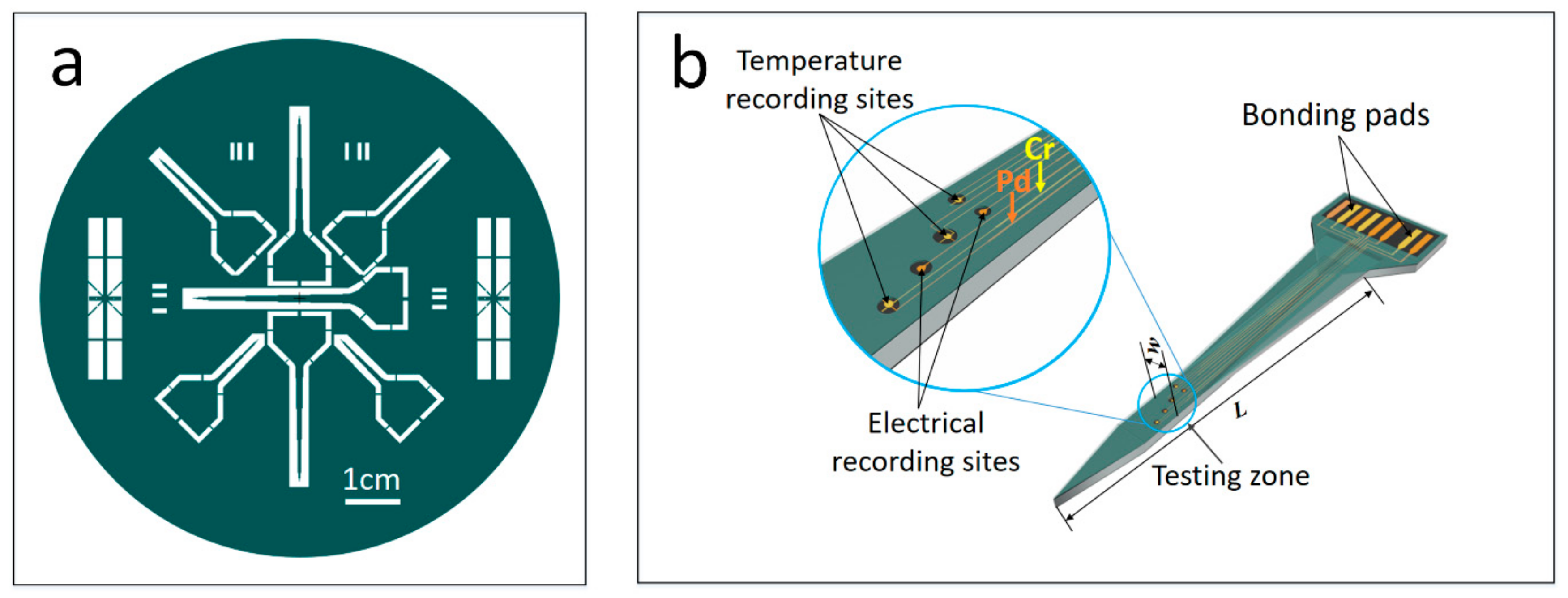
2.2. Design of 3D Probes

Figure 1a shows the overall design of the s.s.-based multifunctional probes. On each 4 in. s.s. wafer, seven sword-shaped probes with varied width and length were patterned. Different widths (w) and lengths (L) were designed to meet different requirements in measuring local temperatures at deep levels and in tissues with varied toughness in animal experiments. The configurations of the w and L parameters were 200 µm and 10.0 mm, 300 µm and 15.0 mm, 400 µm and 20.0 mm, and 500 µm and 30.0 mm. L was defined as the length of the probe from tip to handle, and w was defined as the width close to the probe tip. It should be mentioned that the width of the probe gradually increased from tip to handle, as shown in Figure 1b.
Figure 1b schematically presents the major structure of a freestanding micro-probe with a built-in sensor array of thin-film thermocouple (TFTC) for local temperature measurement and electrodes for electrical signal detection. Each probe consisted of two main parts: a probe body and a connection plate. To ensure that each probe had sufficient mechanical strength, a sword shape was designed with triangular tips and a thickness (t) of 150 µm for all probes.
For the 200 µm-wide probe, two TFTCs and two electrodes were designed. For the 500 µm-wide probes, the number of TFTCs and electrodes was increased to 4–6. To avoid reactions with biological tissue fluids, the TFTC array was covered with a thin oxide layer, while the electrodes were left open at the testing zone.
The connection plate consisted of a triangle with a base length of 1.0 cm and a rectangle with a size of 5.0 mm × 1.0 mm. Its main function was to connect the leads of the TFTC array to the test system.

2.3. Fabrication of Freestanding Microprobes

Figure 2a–h illustrates some major technical processes performed in a standard class-1000 cleanroom for the fabrication of the freestanding microprobes. These complicated processes involved two main steps: (1) defining the shape and position of the probe and fabricating the TFTC array and electrodes; (2) obtaining freestanding microprobes through wet etching.
First, the as-purchased s.s. substrate was cleaned thoroughly as described in Section 2.1 (Figure 2a). Then the substrate was coated with a 3 µm-thick negative photoresist layer of SU-8 (2005, Microchem, Westborough, MA, USA) using a benchtop spin coater (CEEVR 200X, Brewer Science, 4000 rpm, 60 s) and was patterned by photo lithography on a mask aligner (Karl Suss MJB4, Suss, Germany) to define the shapes of the microprobe sword and connection plate (Figure 2b). For this step, soft-baking (95 °C 2.0 min), exposure (to a UV dose of 90 mJ/cm2), post-baking (95 °C, 1.0 min), developing (SU-8 Developer, Microchem, Westborough, MA, USA, 1.0 min), and hard-baking (150 °C, 30 min) were performed in sequence. These were the standard processing parameters for SU-8 2005 [59].
The SU-8 layer was used as an insulating layer to separate the TFTC array and electrodes from the s.s. substrate, and it also reduced the surface roughness thus ensuring a much higher yield of good sensors built on the microprobe.
Next, positive photoresist AR-P 5350 (Allresist, Strausberg, Germany) was used to make TFTC patterns, following our previous procedures [60,61,62,63,64]. A 2 µm-thick AR-R 5350 was spin-coated on top of the front surface at 4000 rpm for 60 s and dried at 110 °C for 3 min. Patterns of TFTC array were carefully aligned with the Karl Suss MJB4 mask aligner to ensure they were located in the center of the probes defined with SU-8 patterns.
After an open window for the deposition of Pd (or Cr) film was created, an oxygen plasma process was performed to remove residual photoresist (Ion Wave 10, PVA TePLa) before thin-film deposition. To improve the bonding strength of the Pd film on the SU-8 layer, a 5 nm-thick Ti thin film was deposited as an adhesion layer. Both Ti layer (5 nm) and Pd layer (thickness 90 nm) were deposited with an electron-beam evaporator (DE400, DE Tec, CN). The Ti–Pd stripe pattern appeared after the lift-off process in acetone (Figure 2c). The circular micro-electrodes for potential electrical measurements were also formed in this layer. A TFTC sensor was made of two different metals, i.e., palladium (Pd) and chromium (Cr) thin films, so the processes for alignment and formation of Pd and Cr patterns and deposition of Pd and Cr thin films were repeated twice. The Cr layer (120 nm) was deposited with a magnetron sputtering system (PVD75, Kurt J. Lesker, USA) in Ar. After lift-off, the TFTC arrays were completely built on the probes (Figure 2d). Then, a thin layer of HfO2 film (20 nm) was sputtered on the TFTC arrays for insulation, while still leaving the circular micro-electrodes testing regions (Figure 1b) open (Figure 2e). Finally, a 3 µm-thick SU-8 layer was patterned on the HfO2 layer to protect the devices from damage. Similarly, a SU-8 layer was spin-coated over the back side of the substrate for protection during etching (Figure 2f).
The wet-etching process was performed after the TFTC arrays and micro-electrodes were fabricated. The s.s. substrates were etched in an acidic solution of FeCl3, HCl, and HNO3, with a mixture of 40.0 g of FeCl3 powder, 16.0 mL of 37.0% HCl, and 16.0 mL of 97.2% HNO3 in 160 mL deionized H2O. A 10 µm-thick positive photoresist (SPR-220, Dow, USA) was used as the mask layer on the SU-8 layer to protect the existing TFTC devices in the wet-etching process. This mask layer was aligned and patterned on the device with standard photolithography processes. Soft-baking of the SPR-220 was done at 115 °C for 90 s (Figure 2g).
The etching was performed at 40 °C in a water bath via the floating technique [65,66]. The total etching period took around 65 min for the sword-shaped probes to thoroughly separate from the substrate. After several thin connecting bridges between each probe and the substrate base were cut with a sharp knife, a 3D freestanding microprobe was ready (Figure 2h).
It should be mentioned that the 150 μm-thick s.s. substrate was not etched through a single process of 65 min. In order to ensure that the device structures of the TFTC and electrodes were not damaged in the etching process (due to over etching in the horizontal direction), after every 5–10 min, the wafer was taken out of the etchant, the SPR-220 photoresist was removed with acetone, and the wafer was rinsed and dried and then covered again with a new layer of SPR-220 photoresist. Alternately, the wafer could be processed after slightly longer time intervals (i.e., 10 min or more), but this increased the risk of breaking the TFTC patterns close to the sides of the probe.

2.4. Device Testing

We calibrated the TFTC arrays on freestanding microprobes in an oil bath through a homemade calibration platform [63,66,67]. During the calibration process, we controlled the oil temperature by heating the hot plate and inserted the sword of the probe into the oil to reach the same temperature. The cold ends of the device were kept at room temperature. The difference in temperature between the hot end and cold end regions was recorded by two identical standard K-type thermocouples. The thermopower outputs of the TFTCs on the probe were measured with one nano-voltmeter (Keithley 2182A) via a multiplexer. The stress–strain measurements were performed on an Instron universal testing machine (Instron, USA). The electrochemical impedance spectroscopy (EIS) was measured with an electrochemical workstation (CHI660e, CH Instruments, USA) in 1x phosphate-buffered saline (PBS, pH 7.4) at room temperature with a three-electrode configuration, where the tested electrodes were working electrodes, while an Ag/AgCl electrode and a large-surface-area platinum wire served as reference and counter electrodes, respectively. During the test, frequency varied from 10 to 100 kHz.
Surface smoothness was investigated with an atomic force microscope (AFM, Dimension Icon, Bruker, Billerica, MA, USA). The morphology of probe and TFTCs was characterized with an optical camera (Axio Scope A1, Carl Zeiss, Oberkochen, Germany) and a scanning electron microscope (SEM, Quanta 600FEG, FEI, Brno, Czech Republic). Elastic measurement of the probes was performed with several pieces of silicon rubber. The sword tip of each probe being tested was mechanically pushed against the rubber surface. The sword part of the probe was bent, and the pushing force was then reduced to check recovery of the sword shape.
In addition, experiments on live animals were performed. Adult male Sprague–Dawley rats (300–350 g) were provided by the Department of Laboratory Animal Sciences, Peking University Health Science Center (Beijing, China). All experimental procedures were approved by the Animal Care and Use Committee of Peking University Health Science Center (LA2017131, approved on March 1, 2017) and were in accordance with the rules of the Declaration of Helsinki of 1975, revised in 2008. Details are given in Supplementary Materials.

3. Results and Discussions

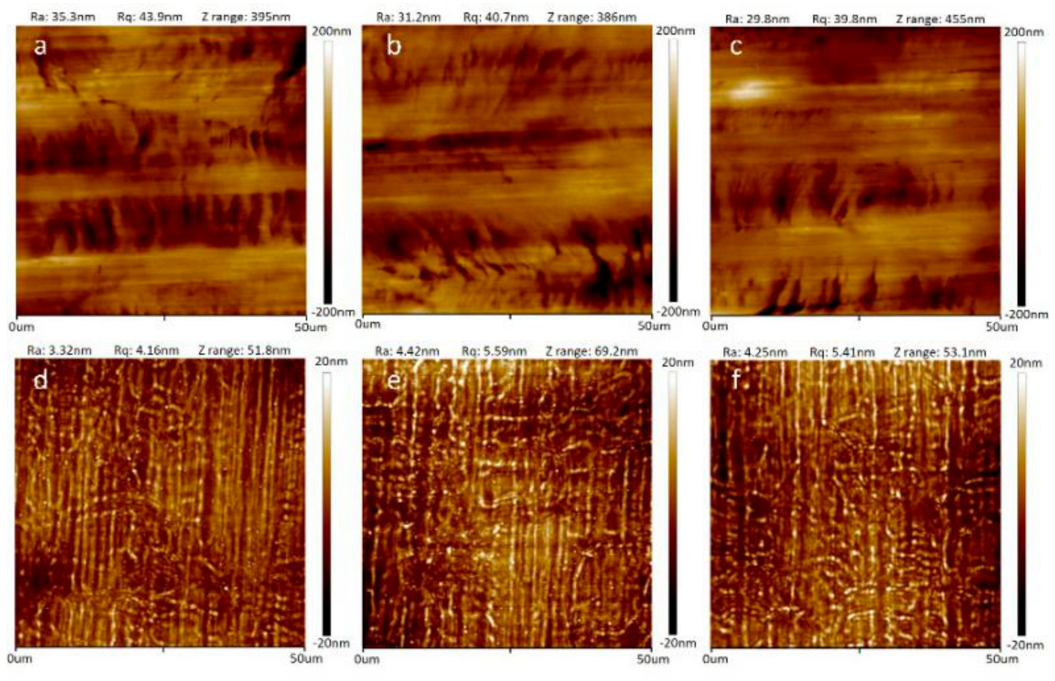
3.1. Improvement of Surface Smoothness after Coating SU-8

The surface of the as-purchased s.s. substrate, although mechanically polished, was rough. Figure 3a–c present typical AFM micrographs of three different regions of an s.s. substrate which underwent the cleaning processes and was ready for the lithography process. The surface was covered with scratch marks resulting from the polishing process with sandpaper. The absolute up and down fluctuation in the Z direction (perpendicular to the surface) was around 380–460 nm. For a scanning area of 50 μm × 50 μm, the root-mean-square roughness was around 40–44 nm.
After being coated with a 3 µm-thick layer of SU-8, surface smoothness improved remarkably. As typically shown in Figure 3d–f, the absolute surface roughness was around 50–70 nm, a sevenfold improvement over the bare s.s. substrate. The root-mean-square roughness was around 4–6 nm for a scanning area of 50 μm × 50 μm, which was a 7–10-times improvement. This SU-8 buffer layer, therefore, not only served as a good insulating layer for the TFTC and micro-electrodes built on the probe but also ensured a better substrate for the following complicated lithography and thin-film deposition processes.

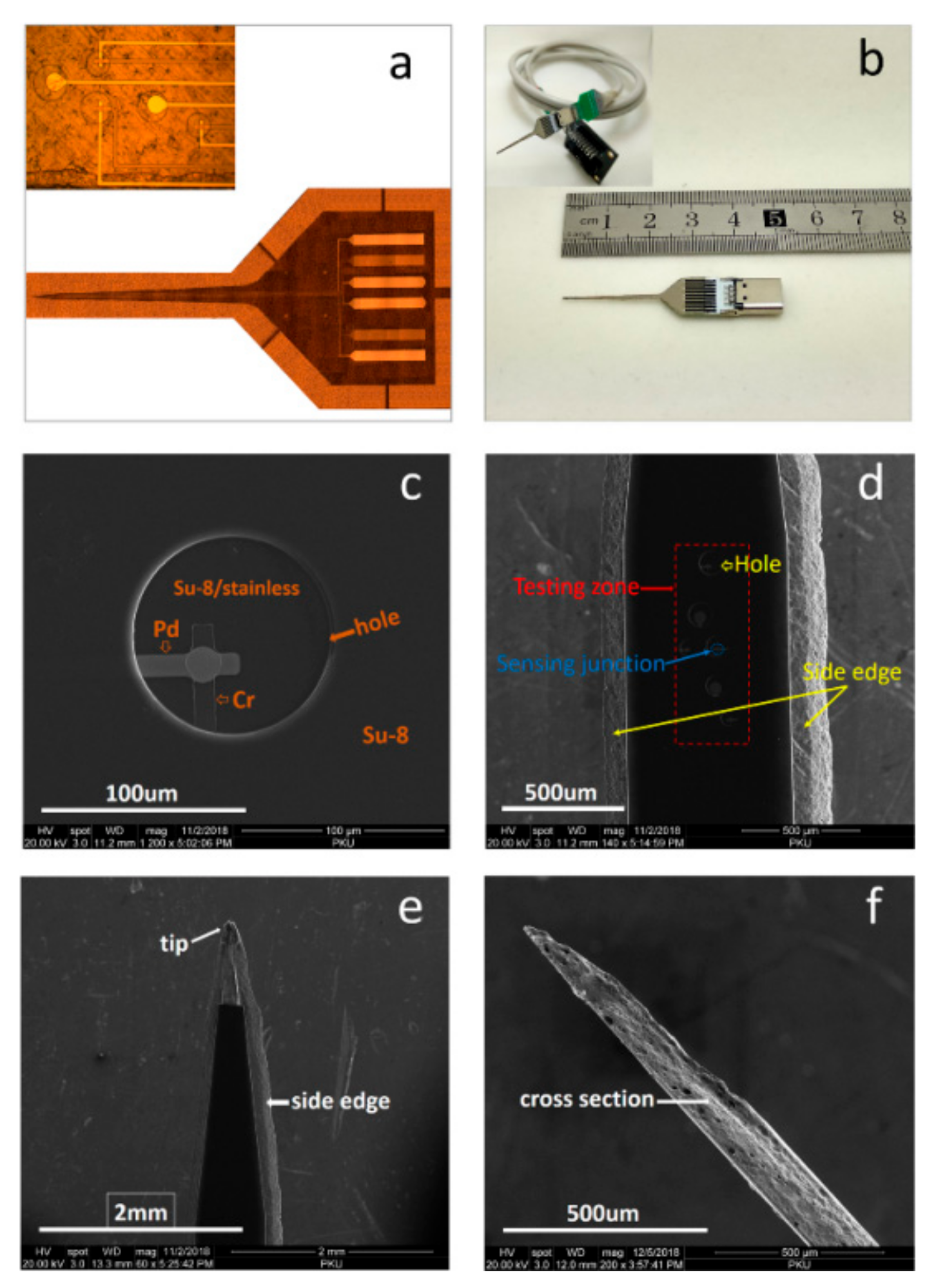
3.2. Lithography and Etching Results

Figure 4 presents optical photographs of two devices. One was a whole 4 in. s.s. wafer before the etching process, where Pd–Cr TFTC arrays were fabricated, and the other was a whole wafer after the etching process, where seven microprobes were clearly defined. The narrow bonding bridges that connected the substrate wafer and the 3D probes are locally shown in the magnified images in Figure 4c,d. These connection bridges helped the probes maintain their original positions on the substrate throughout the fabrication process. After the bridges were cut away from the wafer, we obtained individual freestanding microprobes that were ready for testing.
Figure 5 presents more details of the probes during and after the fabrication process. On each probe, the measurement zones were defined as a circular window in the SU-8 layer. Figure 5a shows optical images of the measurement zones and their locations on the probe. Figure 5b is a photo of a freestanding microprobe assembled in an electrical connection socket. Such a device was ready for practical measurements. Figure 5c is a SEM image of the measurement zone, where the junction of a Pd–Cr TFTC is seen in a circular window of SU-8. Figure 5d is a SEM image for the front part of a freestanding microprobe, where the sensors are seen in the middle of the probe, and the two sides are the etched edges of the s.s. substrate. Figure 5e,f presents SEM micrographs showing the tip and side-view of the sword-like s.s-based microprobes, including the corrosion profiles.

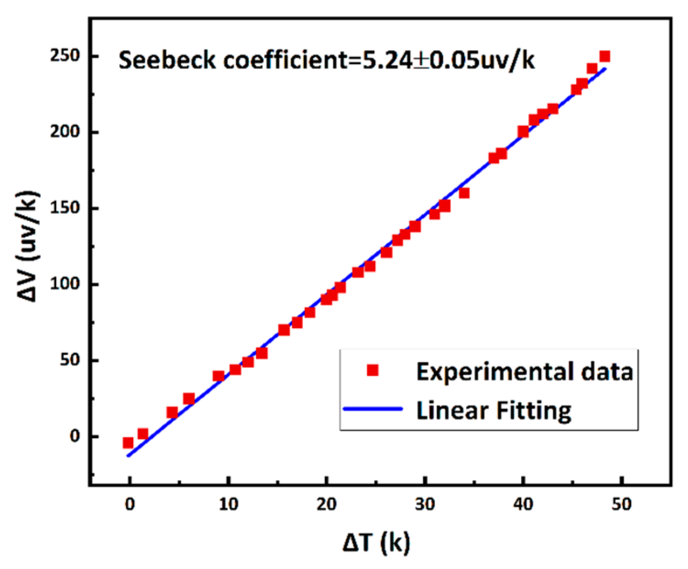
3.3. Sensor Calibration

The TFTCs on freestanding microprobes were calibrated in an oil bath. The outputs of thermopower for each individual Pd–Cr TFTC were measured first at varied temperature differences between its hot and cold ends. The sensitivity of the device was obtained from the slope of a linear fitting of the measured data. Figure 6 shows a typical set of calibration data and the linear fitting. For this device, the sensitivity was approximately 5.24 ± 0.15 µv/k.

3.4. A. C. Impedance

The interface impedance of the electrode–electrolyte system influenced the ability to record neural signals. Figure 7 shows one set of the obtained data. For a typical electrode with 1256 µm2 opening area, the measured low impedance was around 520 kΩ, and the phase was −79.9° at 1 kHz. At higher frequency, the impedance decreased gradually because of the capacitor effect.

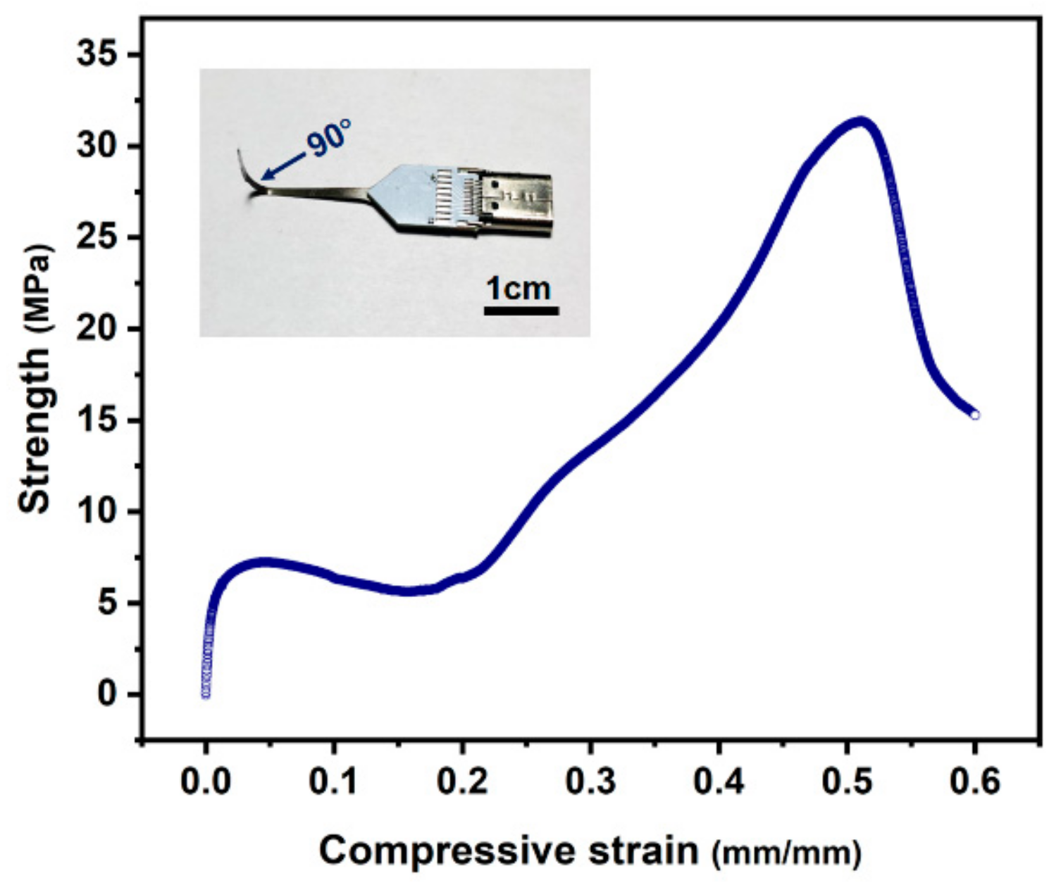
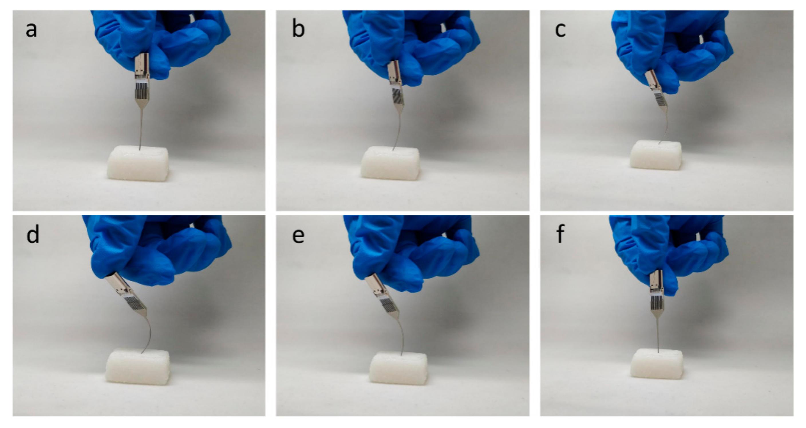
3.5. Testing of Mechanical Strength

The as-fabricated 150 μm-thick freestanding microprobes showed excellent elasticity and mechanical strength. The stress required to bend the stainless-steel probe at 90° was found to be 8.2–95 Mpa, with a standard deviation of 10 MPa, for probes with different lengths. Figure 8 shows one set of the measurement results. The sword part of the probe could be repeatedly bent hundreds of times and still recover to its original shape. Figure 9 shows a testing case, where a probe mounted in its electrical connection socket was pushed against a piece of hard rubber, then the pushing force was released, and the probe returned to the initial straight shape (Video S1). This case proved that stainless-steel probes have better elasticity than silicon-based [35] and glass-based [34] probes.
The mechanical strength of the freestanding microprobes was also tested in live animals. They could be mechanically inserted into tissues of brain, abdomen, and thigh muscles to deep levels at 5–20 mm without causing the probe sword and the sensors on them to break. Moreover, the probes remained straight when they were pulled out of the tough muscle and skin tissues (Figure S1, Video S2). These tests showed that our s.s. probes had excellent mechanical strength with such a thin thickness and performed better than any plastic-based probe [48].

4. Conclusions

In summary, we presented detailed procedures for the fabrication of a freestanding, multifunctional micro-probe made from 150 µm-thick s.s. sheets by using standard cleanroom techniques of photolithography, spin-coating, thin-film deposition, and wet-etching. An array of Pd–Cr TFTCs for temperature measurement and Pd electrodes for electrical measurement were fabricated on top of the sword-shaped s.s. substrate. The probes with length up to 30 mm showed excellent mechanical strength and elastic properties when they were inserted in brain, skin, and muscle tissues of live rats. Calibrations showed that the TFTCs worked well on freestanding microprobes. These novel probes are promising for the deep-level detection of 3D temperature distribution in organs and tissues of live animals and may also serve as deep-level sensors for recording electrical signals in neurons and muscles.

Supplementary Materials

The following are available online at https://www.mdpi.com/1424-8220/19/10/2328/s1, Figure S1: Testing of the freestanding 3D microprobes on live rats, where the probe swards were inserted into tissues of (a) brain, (b) abdomen, and (c) thigh muscles, to deep levels of 5–20 mm. Video S1: Video for the elasticity test of an as-fabricated microprobe with a hard rubber. Video S2: Testing of the freestanding 3D microprobes on live rats, where the probe swards were inserted into and pulled out of the rat brain.

Author Contributions

S.X. and S.Y. conceived the research plan. N.Y. conducted most of the experimental work on device fabrication. Z.W., J.X., and S.Y. prepared early samples. L.G. performed the AFM analysis of the devices. Z.T. performed SEM measurements. Y.Z. and M.Y. performed the experiments on mice. N.Y. performed electrochemical measurements. N.Y. and S.X. interpreted the data and wrote the paper. All authors have reviewed and approved the final manuscript.

Funding

This work was financially supported by the National Key R&D Program of China (Grants No. 2017YFA0701302 and No. 2016YFA0200802).

Acknowledgements

We are grateful to You Wan and Fengyu Liu for offering lab facilities for the experiments on rats. We thank Anyuan Cao and Yawei Yang for help in mechanical stress–strain measurements. We thank Xiaojie Duan and Xuefeng Fu for help in electrochemical measurements. We thank George for revising the grammar and sentences of the manuscript.

Conflicts of Interest

The authors declare that they have no competing interests.

Ethical Approval

All experimental procedures were approved by the Animal Care and Use Committee of Peking University Health Science Center (LA2017131, approved on March 1, 2017) and were in accordance with the rules of the Declaration of Helsinki of 1975, revised in 2008.

References

  1. Kim, D.H.; Lu, N.; Ghaffari, R.; Kim, Y.S.; Lee, S.P.; Xu, L.; Wu, J.; Kim, R.H.; Song, J.; Liu, Z.; et al. Materials for multifunctional balloon catheters with capabilities in cardiac electrophysiological mapping and ablation therapy. Nat. Mater. 2011, 10, 316–323. [Google Scholar] [CrossRef] [Green Version]
  2. Kim, D.H.; Viventi, J.; Amsden, J.J.; Xiao, J.; Vigeland, L.; Kim, Y.S.; Blanco, J.A.; Panilaitis, B.; Frechette, E.S.; Contreras, D.; et al. Dissolvable films of silk fibroin for ultrathin conformal bio-integrated electronics. Nat. Mater. 2010, 9, 511–517. [Google Scholar] [CrossRef] [PubMed] [Green Version]
  3. Kim, D.H.; Ahn, J.H.; Choi, W.M.; Kim, H.S.; Kim, T.H.; Song, J.; Huang, Y.Y.; Liu, Z.; Lu, C.; Rogers, J.A. Stretchable and foldable silicon integrated circuits. Science 2008, 320, 507–511. [Google Scholar] [CrossRef] [PubMed]
  4. Kim, D.H.; Song, J.; Choi, W.M.; Kim, H.S.; Rogers, J.A. Materials and noncoplanar mesh designs for integrated circuits with linear elastic responses to extreme mechanical deformations. Proc. Nat. Acad. Sci. USA 2008, 105, 18675–18680. [Google Scholar] [CrossRef] [PubMed] [Green Version]
  5. Viventi, J.; Kim, D.H.; Vigeland, L.; Frechette, E.S.; Blanco, J.A.; Kim, Y.S.; Avrin, A.E.; Tiruvadi, V.R.; Hwang, S.W.; Vanleer, A.C.; et al. Flexible, foldable, actively multiplexed, high-density electrode array for mapping brain activity in vivo. Nat. Neurosci. 2011, 14, 1599–1605. [Google Scholar] [Green Version]
  6. Kim, D.H.; Ghaffari, R.; Lu, N.; Rogers, J.A. Flexible and stretchable electronics for biointegrated devices. Annu. Rev. Biomed. Eng. 2012, 14, 113–128. [Google Scholar] [CrossRef] [PubMed]
  7. Cavazos Sepulveda, A.C.; Diaz Cordero, M.S.; Carreño, A.A.A.; Nassar, J.M.; Hussain, M.M. Stretchable and foldable silicon-based electronics. Appl. Phys. Lett. 2017, 110, 134103. [Google Scholar] [CrossRef]
  8. Chen, C.H.; Chuang, S.C.; Lee, Y.T.; Chang, Y.C.; Yeh, S.R.; Yao, D.J. Three-dimensional flexible microprobe for recording the neural signal. In Proceedings of the IEEE International Conference on Nano/Molecular Medicine & Engineering, Tainan, Taiwan, 18–21 October 2010. [Google Scholar]
  9. Chen, C.H.; Chuang, S.C.; Su, H.C.; Hsu, W.L.; Yew, T.R.; Chang, Y.C.; Yeh, S.R.; Yao, D.J. A three-dimensional flexible microprobe array for neural recording assembled through electrostatic actuation. Lab Chip 2011, 11, 1647–1655. [Google Scholar] [CrossRef]
  10. Tan, K.L.; Chen, W.; Damalerio, R.; Lim, R.; Chungpaiboonpatana, S.; Cheng, M.Y. Evaluation of biodegradable coating on the stiffness control of the polyimide-based probe used in neural devices. In Proceedings of the IEEE Electronics Packaging & Technology Conference, Singapore, 2–4 December 2015. [Google Scholar]
  11. Kuo, J.T.; Kim, B.J.; Hara, S.A.; Lee, C.D.; Gutierrez, C.A.; Hoang, T.Q.; Meng, E. Novel flexible Parylene neural probe with 3D sheath structure for enhancing tissue integration. Lab Chip 2013, 13, 554–561. [Google Scholar] [CrossRef]
  12. Kim, B.J.; Kuo, J.T.; Hara, S.A.; Lee, C.D.; Yu, L.; Gutierrez, C.A.; Hoang, T.Q.; Pikov, V.; Meng, E. 3D Parylene sheath neural probe for chronic recordings. J. Neural Eng. 2013, 10, 045002. [Google Scholar] [CrossRef] [PubMed]
  13. Duan, X.; Lieber, C.M. Nanoelectronics meets biology: From new nanoscale devices for live-cell recording to 3D innervated tissues. Chem. Asian J. 2013, 8, 2304–2314. [Google Scholar] [CrossRef] [PubMed]
  14. Hong, G.; Viveros, R.D.; Zwang, T.J.; Yang, X.; Lieber, C.M. Tissue-like neural probes for understanding and modulating the brain. Biochemistry 2018, 57, 3995–4004. [Google Scholar] [CrossRef] [PubMed]
  15. Dai, X.; Hong, G.; Gao, T.; Lieber, C.M. Mesh nanoelectronics: Seamless integration of electronics with tissues. Acc. Chem. Res. 2018, 51, 309–318. [Google Scholar] [CrossRef] [PubMed]
  16. Hong, G.; Yang, X.; Zhou, T.; Lieber, C.M. Mesh electronics: A new paradigm for tissue-like brain probes. Curr. Opin. Neurobiol. 2018, 50, 33–41. [Google Scholar] [CrossRef]
  17. Duan, X.; Fu, T.M.; Liu, J.; Lieber, C.M. Nanoelectronics-biology frontier: From nanoscopic probes for action potential recording in live cells to three-dimensional cyborg tissues. Nano Today 2013, 8, 351–373. [Google Scholar] [CrossRef] [Green Version]
  18. Xie, C.; Liu, J.; Fu, T.-M.; Dai, X.; Zhou, W.; Lieber, C.M. Three-dimensional macroporous nanoelectronic networks as minimally invasive brain probes. Nat. Mater. 2015, 14, 1286–1292. [Google Scholar] [CrossRef] [Green Version]
  19. Goßler, C.; Bierbrauer, C.; Moser, R.; Kunzer, M.; Holc, K.; Pletschen, W.; Köhler, K.; Wagner, J.; Schwaerzle, M.; Ruther, P.; et al. GaN-based micro-LED arrays on flexible substrates for optical cochlear implants. J. Phys. D Appl. Phys. 2014, 47, 205401. [Google Scholar] [CrossRef]
  20. Knisely, K.; Zhao, C.; Grosh, K. A MEMS AlN transducer array with flexible interconnections for use as a cochlear implant. AIP Conf. Proc. 2015, 1703, 100004. [Google Scholar]
  21. Rousche, P.J.; Pellinen, D.S.; Pivin, D.P.; Williams, J.C.; Vetter, R.J.; Kipke, D.R. Flexible polyimide-based intracortical electrode arrays with bioactive capability. IEEE Trans. Biomed. Eng. 2001, 48, 361–371. [Google Scholar] [CrossRef]
  22. Wise, K.D.; Angell, J.B.; Starr, A. An integrated-circuit approach to extracellular microelectrodes. IEEE Trans. Biomed. Eng. 1970, BME-17, 238–247. [Google Scholar] [CrossRef]
  23. Xu, C.; Lemon, W.; Liu, C. Design and fabrication of a high-density metal microelectrode array for neural recording. Sensor. Actuators A (Phys.) 2002, 96, 78–85. [Google Scholar] [CrossRef]
  24. Ensell, G.; Banks, D.J.; Ewins, D.J.; Balachandran, W.; Richards, P.R. Silicon-based microelectrodes for neurophysiology fabricated using a gold metallization/nitride passivation system. J. Microelectromech. Syst. 1996, 5, 117–121. [Google Scholar] [CrossRef]
  25. Anderson, D.J.; Najafi, K.; Tanghe, S.J.; Evans, D.A.; Levy, K.L.; Hetke, J.F.; Xue, X.L.; Zappia, J.J.; Wise, K.D. Batch-fabricated thin-film electrodes for stimulation of the central auditory system. IEEE Trans. Biomed. Eng. 1989, 36, 693–704. [Google Scholar] [CrossRef]
  26. Kovacs, G.T.; Storment, C.W.; Rosen, J.M. Regeneration microelectrode array for peripheral nerve recording and stimulation. IEEE Trans. Biomed. Eng. 1992, 39, 893–902. [Google Scholar] [CrossRef]
  27. Kipke, D.R.; Pellinen, D.S.; Vetter, R.J. Advanced neural implants using thin-film polymers. In Proceedings of the IEEE International Symposium on Circuits & Systems, Phoenix-Scottsdale, AZ, USA, 26–29 May 2002. [Google Scholar]
  28. Norlin, P.; Kindlundh, M.; Mouroux, A.; Yoshida, K.; Hofmann, U.G. A 32-site neural recording probe fabricated by DRIE of SOI substrates. J. Micromech. Microeng. 2002, 12, 414–419. [Google Scholar] [CrossRef] [Green Version]
  29. Baldwin, H.A.; Frenk, S.; Lettvin, J.Y. Glass-coated tungsten microelectrodes. Science 1965, 148, 1462–1464. [Google Scholar] [CrossRef] [PubMed]
  30. Fomani, A.A.; Moradi, M.; Assaf, S.; Mansour, R.R. 3D Microprobes for deep brain stimulation and recording. In Proceedings of the 2010 Annual International Conference of the IEEE Engineering in Medicine and Biology, Buenos Aires, Argentina, 31 August–3 September 2010. [Google Scholar]
  31. Motta, P.S.; Judy, J.W. Multielectrode microprobes for deep-brain stimulation fabricated with a customizable 3-D electroplating process. IEEE Trans. Biomed. Eng. 2005, 52, 923–933. [Google Scholar] [CrossRef] [PubMed]
  32. Wang, R.; Medioni, G.; Winstein, C.J.; Blanco, C. Home monitoring musculo-skeletal disorders with a single 3D sensor. In Proceedings of the 2013 IEEE Conference on Computer Vision and Pattern Recognition Workshops, Portland, OR, USA, 23–28 June 2013; pp. 521–528. [Google Scholar]
  33. Lee, S.; Ahn, J.H.; Seo, J.M.; Chung, H.; Cho, D.I. Electrical characterization of 3D Au microelectrodes for use in retinal prostheses. Sensors (Basel) 2015, 15, 14345–14355. [Google Scholar] [CrossRef]
  34. Lee, Y.T.; Lin, C.W.; Lin, C.M.; Yeh, S.R.; Chang, Y.C.; Fu, C.C.; Fang, W. A 3D glass microprobe array with embedded silicon for alignment and electrical connection. In Proceedings of the Solid-state Sensors, Actuators & Microsystems Conference, Denver, CO, USA, 21–25 June 2009. [Google Scholar]
  35. Jones, K.E.; Campbell, P.K.; Normann, R.A. A glass/silicon composite intracortical electrode array. Ann. Biomed. Eng. 1992, 20, 423–437. [Google Scholar] [CrossRef]
  36. Topper, M.; Klein, M.; Buschick, K.; Glaw, V.; Solzbacher, F. Biocompatible hybrid flip chip microsystem integration for next generation wireless neural interfaces. In Proceedings of the Electronic Components & Technology Conference, San Diego, CA, USA, 30 May–2 June 2006. [Google Scholar]
  37. Lin, C.-W.; Hsu, C.-P.; Yang, H.-A.; Wang, W.C.; Fang, W. Implementation of silicon-on-glass MEMS devices with embedded through-wafer silicon vias using the glass reflow process for wafer-level packaging and 3D chip integration. J. Micromech. Microeng. 2008, 18, 025018. [Google Scholar] [CrossRef]
  38. Sohee, K.; Tathireddy, P.; Normann, R.A.; Solzbacher, F. Thermal impact of an active 3-D microelectrode array implanted in the brain. IEEE Trans. Neural Syst. Rehab. Eng. 2007, 15, 493–501. [Google Scholar] [CrossRef]
  39. Kim, S.; Zoschke, K.; Klein, M.; Black, D.; Buschick, K.; Toepper, M.; Tathireddy, P.; Harrison, R.; Oppermann, H.; Solzbacher, F. Switchable polymer-based thin film coils as a power module for wireless neural interfaces. Sensor. Actuators A (Phys.) 2007, 136, 467–474. [Google Scholar] [CrossRef] [PubMed]
  40. Matin, M.A.; Ikedo, A.; Kawano, T.; Sawada, K.; Ishida, M. Microscale temperature sensing using novel reliable silicon vertical microprobe array: Computation and experiment. Microelectron. Reliab. 2015, 55, 2689–2697. [Google Scholar] [CrossRef]
  41. Campbell, P.K.; Jones, K.E.; Huber, R.J.; Horch, K.W.; Normann, R.A. A silicon-based, three-dimensional neural interface: Manufacturing processes for an intracortical electrode array. IEEE Trans. Biomed. Eng. 1991, 38, 758–768. [Google Scholar] [CrossRef] [PubMed]
  42. Jun, J.J.; Steinmetz, N.A.; Siegle, J.H.; Denman, D.J.; Bauza, M.; Barbarits, B.; Lee, A.K.; Anastassiou, C.A.; Andrei, A.; Aydın, Ç.J.N. Fully integrated silicon probes for high-density recording of neural activity. Nature 2017, 551, 232–236. [Google Scholar] [CrossRef] [PubMed]
  43. Jonathan, V.; Dae-Hyeong, K.; Moss, J.D.; Yun-Soung, K.; Blanco, J.A.; Nicholas, A.; Andrew, H.; Xiao, J.; Huang, Y.; Callans, D.J. A conformal, bio-interfaced class of silicon electronics for mapping cardiac electrophysiology. Sci. Transl. Med. 2010, 2, 22–24. [Google Scholar]
  44. Usmanov, D.T.; Ninomiya, S.; Hiraoka, K.; Wada, H.; Nakano, H.; Matsumura, M.; Sanada-Morimura, S.; Nonami, H. Electrospray generated from the tip-sealed fine glass capillary inserted with an acupuncture needle electrode. J. Am. Soc. Mass. Spectrom. 2018, 29, 2297–2304. [Google Scholar] [CrossRef] [PubMed]
  45. Stavrinidis, G.; Michelakis, K.; Kontomitrou, V.; Giannakakis, G.; Sevrisarianos, M.; Sevrisarianos, G.; Chaniotakis, N.; Alifragis, Y.; Konstantinidis, G. SU-8 microneedles based dry electrodes for electroencephalogram. Microelectron. Eng. 2016, 159, 114–120. [Google Scholar] [CrossRef]
  46. Herwik, S.; Holzhammer, T.; Paul, O.; Ruther, P. Out-of-plane assembly of 3D neural probe arrays using a platform with SU8-based thermal actuators. In Proceedings of the Solid-state Sensors, Actuators & Microsystems Conference, Beijing, China, 5–9 June 2011. [Google Scholar]
  47. Martinez, V.; Behr, P.; Drechsler, U.; Polesel-Maris, J.; Potthoff, E.; Vörös, J.; Zambelli, T. SU-8 hollow cantilevers for AFM cell adhesion studies. J. Micromech. Microeng. 2016, 26, 055006. [Google Scholar] [CrossRef] [Green Version]
  48. Takano, N.; Tachikawa, H.; Miyano, T.; Nishiyabu, K. Insertion testing of polyethylene glycol microneedle array into cultured human skin with biaxial tension. J. Sol. Mech. Mater. Eng. 2009, 3, 604–612. [Google Scholar] [CrossRef]
  49. Tan, K.L.; Cheng, M.Y.; Chen, W.G.; Rui, Q.L.; Damalerio, M.R.B.; Yao, L.; Li, P.; Gu, Y.D.; Min, K.J. Polyethylene glycol-coated polyimide-based probe with neural recording IC for chronic neural recording. Adv. Mater. Res. 2013, 849, 183–188. [Google Scholar] [CrossRef]
  50. Chen, P.C.; Lal, A. Detachable ultrasonic enabled inserter for neural probe insertion using biodissolvable Polyethylene Glycol. In Proceedings of the Transducers-International Conference on Solid-state Sensors, Anchorage, AK, USA, 21–25 June 2015. [Google Scholar]
  51. Zhou, K.; Li, Y.; Peng, Y.; Cui, X.; Dai, J.; Cui, M. Structure-property relationships of polyethylene glycol modified fluorophore as near-Infrared abeta imaging probes. Anal. Chem. 2018, 90, 8576–8582. [Google Scholar] [CrossRef]
  52. Follstaedt, D.M.; Yost, F.G.; Pope, L.E.; Picraux, S.T.; Knapp, J.A. The amorphous phase and surface mechanical properties of 304 stainless steel implanted with Ti and C. Appl. Phys. Lett. 1983, 43, 358–360. [Google Scholar] [CrossRef]
  53. Xia, Y.T.; Liu, X.; Han, D.; Han, Z.F. Improvement of mechanical properties of martensitic stainless steel by plasma nitriding at low temperature. Acta. Metall. Sin. (Engl. Lett.) 2008, 21, 21–29. [Google Scholar] [CrossRef]
  54. Nie, F.L.; Wang, S.G.; Wang, Y.B.; Wei, S.C.; Zheng, Y.F. Comparative study on corrosion resistance and in vitro biocompatibility of bulk nanocrystalline and microcrystalline biomedical 304 stainless steel. Dent. Mater. 2011, 27, 677–683. [Google Scholar] [CrossRef] [PubMed]
  55. Wang, G.; Ge, S.; Yang, S.; Wang, H.; Dong, Q.; Qin, Z.; Gao, J.; Yong, W. Study on the biodegradability and biocompatibility of WE magnesium alloys. Mater. Sci. Eng. C 2012, 32, 2190–2198. [Google Scholar] [CrossRef]
  56. In, S.L.; Gwak, Y.S.; Kim, H.R.; Razzaq, A.; Lee, K.S.; Kim, H.Y.; Chang, S.; Lee, B.H.; Grimes, C.A.; Yang, C.H. Hierarchical micro/nano-porous acupuncture needles offering enhanced therapeutic properties. Sci. Rep. 2016, 6, 34061. [Google Scholar] [CrossRef] [PubMed]
  57. Feng, R.; Farris, R.J. The characterization of thermal and elastic constants for an epoxy photoresist SU8 coating. J. Mater. Sci. 2002, 37, 4793–4799. [Google Scholar] [CrossRef]
  58. Athanasoulia, I.-G.; Tarantili, P.A. Preparation and characterization of polyethylene glycol/poly(L-lactic acid) blends. Pure Appl. Chem. 2017, 89, 141–152. [Google Scholar] [CrossRef]
  59. Internet SU-8 2000 Permanent Epoxy Negative Photoresist processing guidelines for:SU-8 2000.5, SU-8 2002, SU-8 2005, SU-8 2007, SU-8 2010 and SU-8 2015 [internet]. Available online: http://www.microchem.com/Prod-SU82000.htm (accessed on 8 January 2019).
  60. Fan, Y.; Yang, N.; Huo, X.; Xu, S. Thermal sensing in fluid at the micro-nano-scales. Biomicrofluidics 2018, 12, 041501. [Google Scholar]
  61. Yang, F.; Li, G.; Yang, J.; Wang, Z.; Han, D.; Zheng, F.; Xu, S. Measurement of local temperature increments induced by cultured HepG2 cells with micro-thermocouples in a thermally stabilized system. Sci. Rep. 2017, 7, 1721. [Google Scholar] [CrossRef]
  62. Han, D.; Li, G.; Zhou, S.; Wang, Z.; Yang, F.; Xu, S. To save half contact pads in 2D mapping of local temperatures with a thermocouple array. RSC Adv. 2017, 7, 9100–9105. [Google Scholar] [CrossRef] [Green Version]
  63. Liu, H.; Sun, W.; Chen, Q.; Xu, S. Thin-film thermocouple array for time-resolved local temperature mapping. IEEE Electr. Device Lett. 2011, 32, 1606–1608. [Google Scholar] [CrossRef]
  64. Xu, J.J.; Lei, Z.J.; Guo, J.K.; Huang, J.; Wang, W.; Reibetanz, U.; Xu, S.Y. Trapping and driving individual charged micro-particles in fluid with an electrostatic device. Nanomicro Lett. 2016, 8, 270–281. [Google Scholar] [CrossRef]
  65. Han, D.H.; Xu, J.J.; Wang, Z.H.; Yang, N.; Li, X.Z.; Qian, Y.Y.; Li, G.; Dai, R.J.; Xu, S. Penetrating effect of high-intensity infrared laser pulses through body tissue. RSC Adv. 2018, 8, 32344–32357. [Google Scholar] [CrossRef]
  66. Wang, Z.; Yang, F.; Han, D.; Li, G.; Xu, J.; Xu, S. Alternative method to fabricate microdevices on a freestanding Si3N4 window. J. Vac. Sci. Technol. B 2017, 35, 041601. [Google Scholar] [CrossRef]
  67. Li, G.; Wang, Z.; Mao, X.; Zhang, Y.; Huo, X.; Liu, H.; Xu, S. Real-time two-dimensional mapping of relative local surface temperatures with a thin-film sensor array. Sensors (Basel) 2016, 16, 977. [Google Scholar] [CrossRef]
Figure 1. (a) Overall design of seven 3D micro-probes on a 4 in.-diameter s.s. substrate. (b) Schematic figure of the structure of a multifunctional 3D micro-probe.
Sensors 19 02328 g001
Figure 2. Illustration of the fabrication processes of a multifunctional 3D micro-probe. (a) Cleaned stainless-steel (s.s.) substrate. (b) Patterns of the probes with SU-8. (c) Ti–Pd patterns on the probes. (d) Cr patterns added to complete the Pd–Cr thin-film thermocouples (TFTCs) on the probes. (e) Covering with a HfO2 insulating layer, leaving testing opening windows. (f) Additional SU-8 layer to protect the TFTCs. (g) Coating of a mask layer of SPR-220 for the etching process. (h) The s.s. substrate was etched thoroughly after 65 min and cut from the substrate, resulting in a freestanding 3D probe.
Sensors 19 02328 g002
Figure 3. AFM micrographs of the substrate surfaces. (a)–(c) Results taken from a cleaned bare SUS 304 s.s. surface. (d)–(f) Results taken from the s.s. substrate covered with a 3 μm-thick SU-8 resist layer.
Sensors 19 02328 g003
Figure 4. Optical photographs of the devices during the fabrication process. (a) A whole 4 in. substrate with fabricated TFTC arrays. (b) A whole substrate after the etching process. (c) An enlarged local area showing a narrow bonding bridge connecting the substrate and the 3D probe. (d) A close look at a bonding bridge after the etching process was completed, showing the probes still fixed in their original positions on the substrate.
Sensors 19 02328 g004
Figure 5. Optical images and scanning electron microscopy images of the as-fabricated device and assembled device. (a) Measurement zones on the probe before the etching process. (b) A microprobe assembled in an electrical connection socket. (c) SEM image of a measurement zone. (d) SEM image of the front part of a microprobe. (e) SEM micrograph of a probe tip. (f) SEM side-view of a probe tip.
Sensors 19 02328 g005
Figure 6. Calibration results for the Pd–Cr TFTC on a 3D microprobe.
Sensors 19 02328 g006
Figure 7. A typical electrochemical impedance spectroscopy of a Pd electrode.
Sensors 19 02328 g007
Figure 8. A typical stress–strain curve under compression for an as-fabricated 20 mm-long freestanding probe (shown in the inset).
Sensors 19 02328 g008
Figure 9. Photographs for the elasticity test of an as-fabricated microprobe with a hard rubber.
Sensors 19 02328 g009

