A Radiation-Hardened SAR ADC with Delay-Based Dual Feedback Flip-Flops for Sensor Readout Systems


Abstract
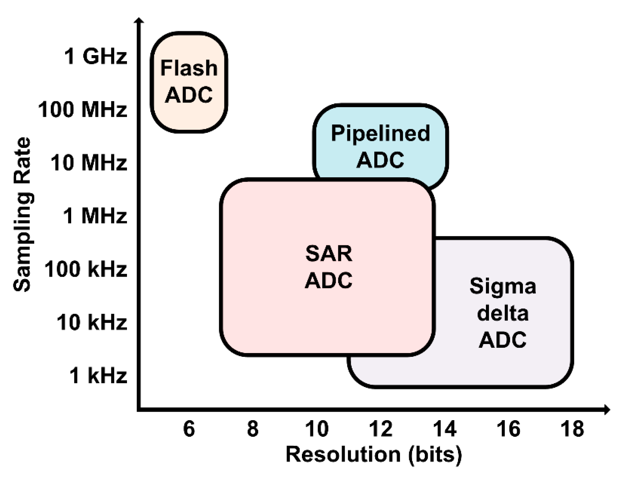
:1. Introduction
2. Radiation-Hardened ADC Structure
- Digital-to-analog converter (DAC): A capacitor DAC commonly used in SAR ADCs can significantly reduce the accuracy due to voltage changes in capacitors caused by SEE. Therefore, this paper adopts a resistor-type DAC that can be robust to SEE.
- Sample-and-hold circuit (S/H): The sampling capacitor was set as large as possible within a given operation speed to minimize the voltage changes in capacitors due to SEE.
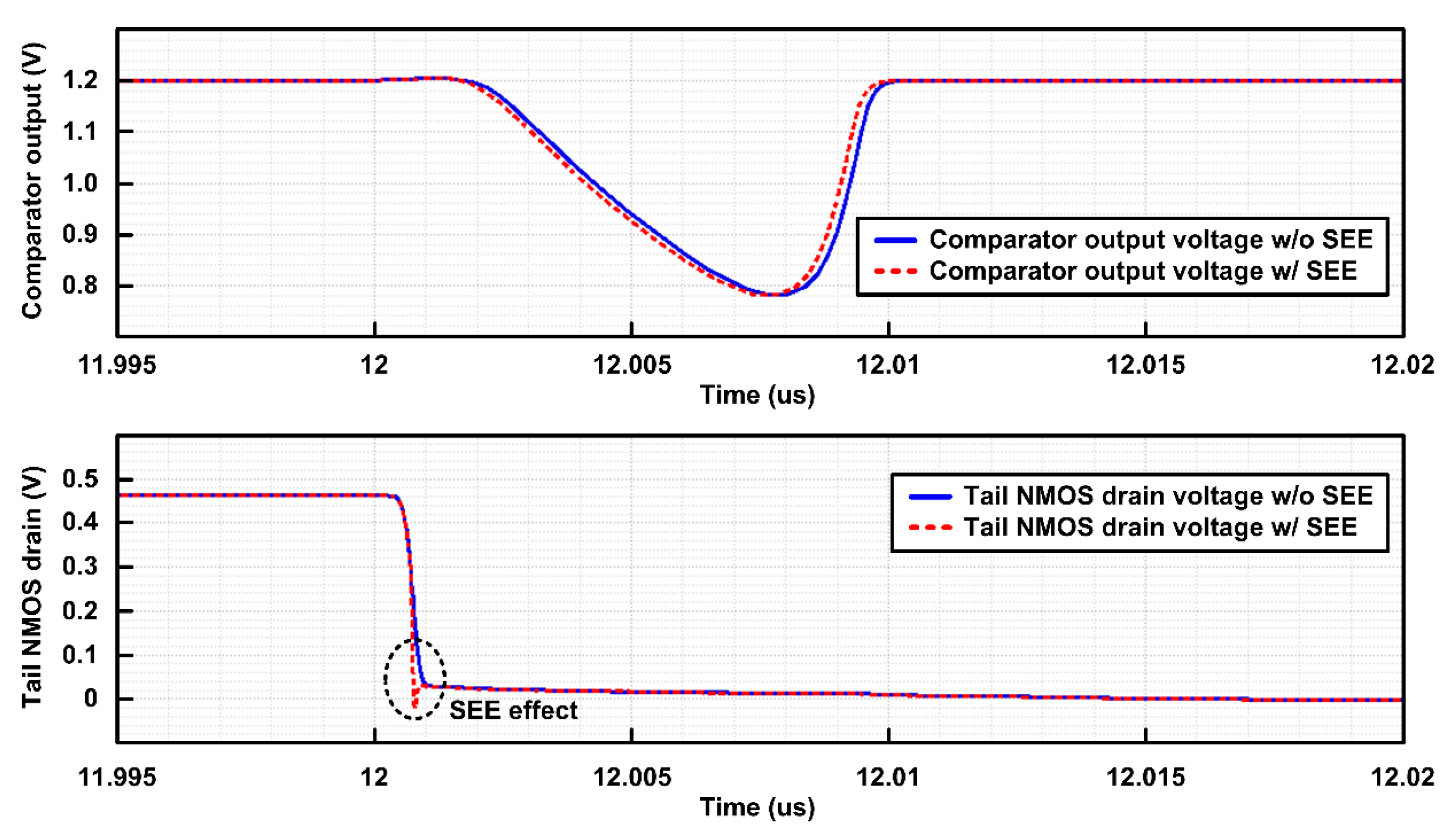
- Comparator: A strong-arm digital comparator, which is robust against transistor variations by TID, is used [10]. The input stage utilizes both n-channel metal-oxide-semiconductor (NMOS) and p-channel metal-oxide-semiconductor (PMOS) pairs to have a wide input range. Also, the TID monitoring function inside the comparator automatically measures Vth variation in transistors and adjusts the gate voltage to compensate for TID on transistors [11].
- SAR logic: Conventional flip-flops used in the SAR logic circuit suffer from data flip due to SEE, which leads to soft errors [12]. To reduce the soft error rate, the proposed radiation-hardened flip-flops were adopted in the SAR logic circuit.
3. Radiation-Hardened Flip-Flop with Delay-Based Dual Feedback Loops
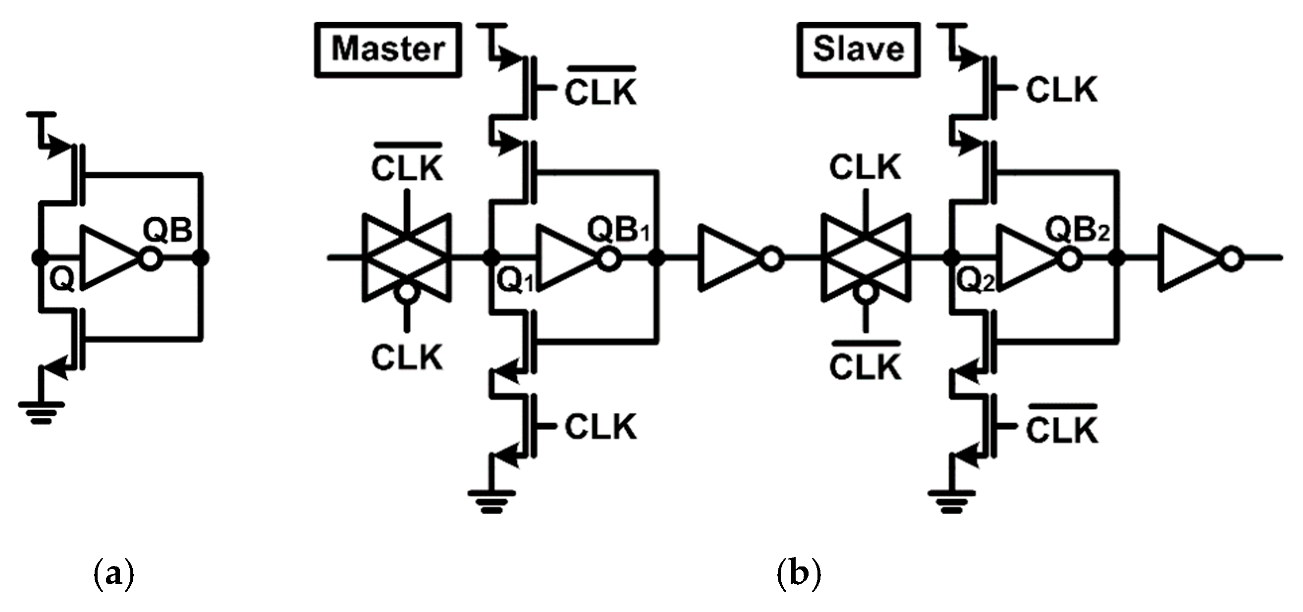
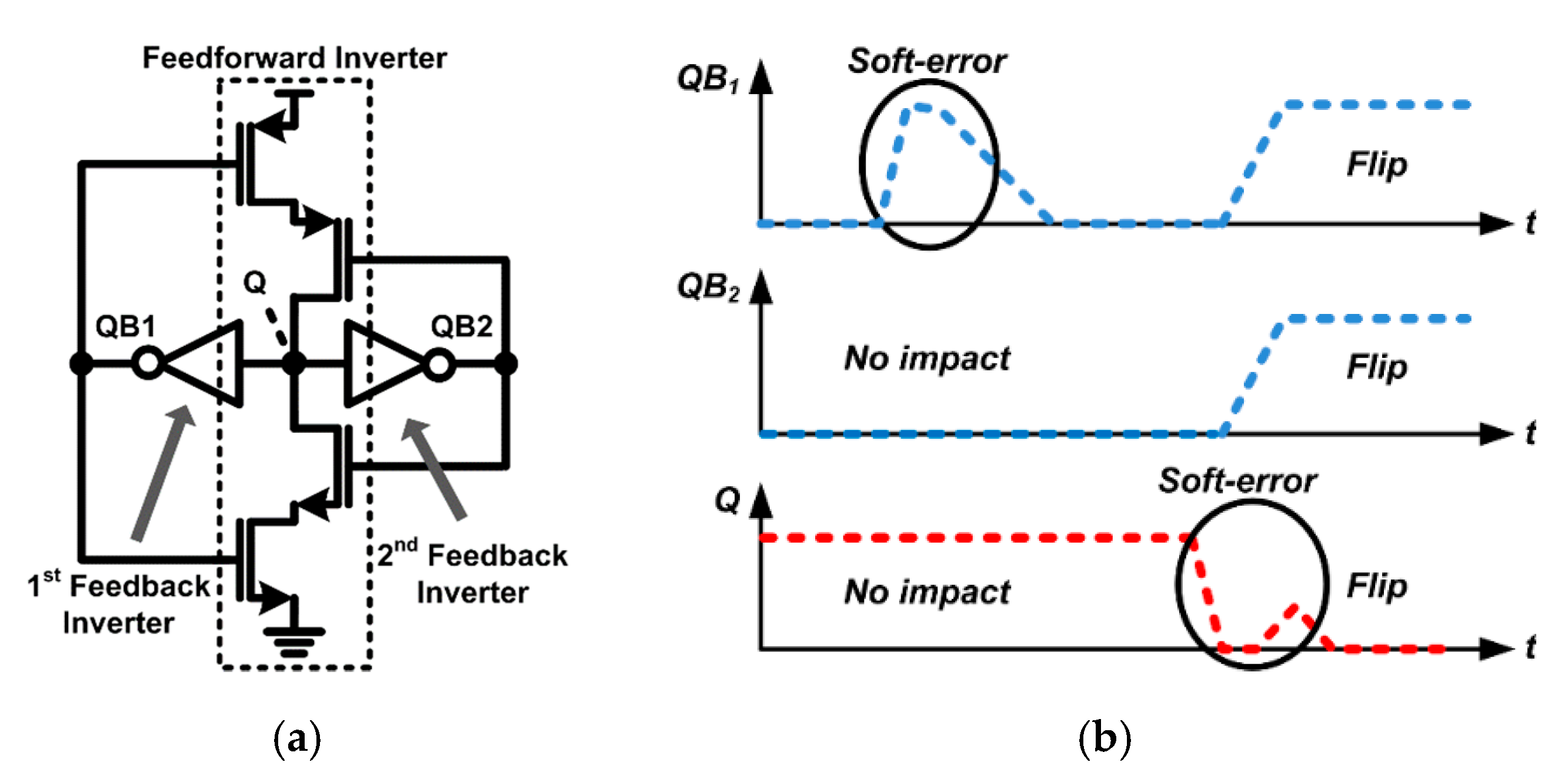
3.1. Limitations of Conventional Flip-Flops
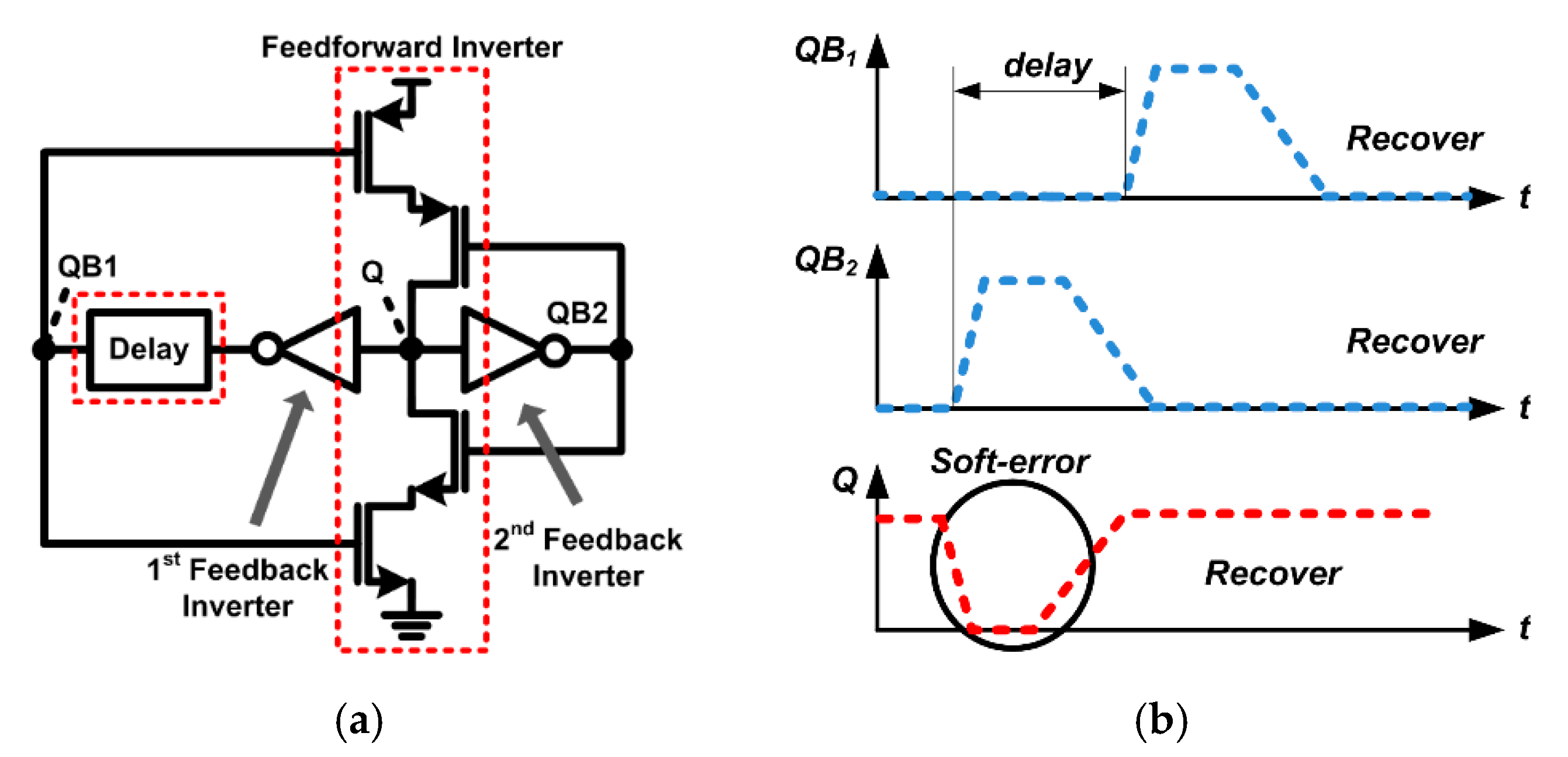
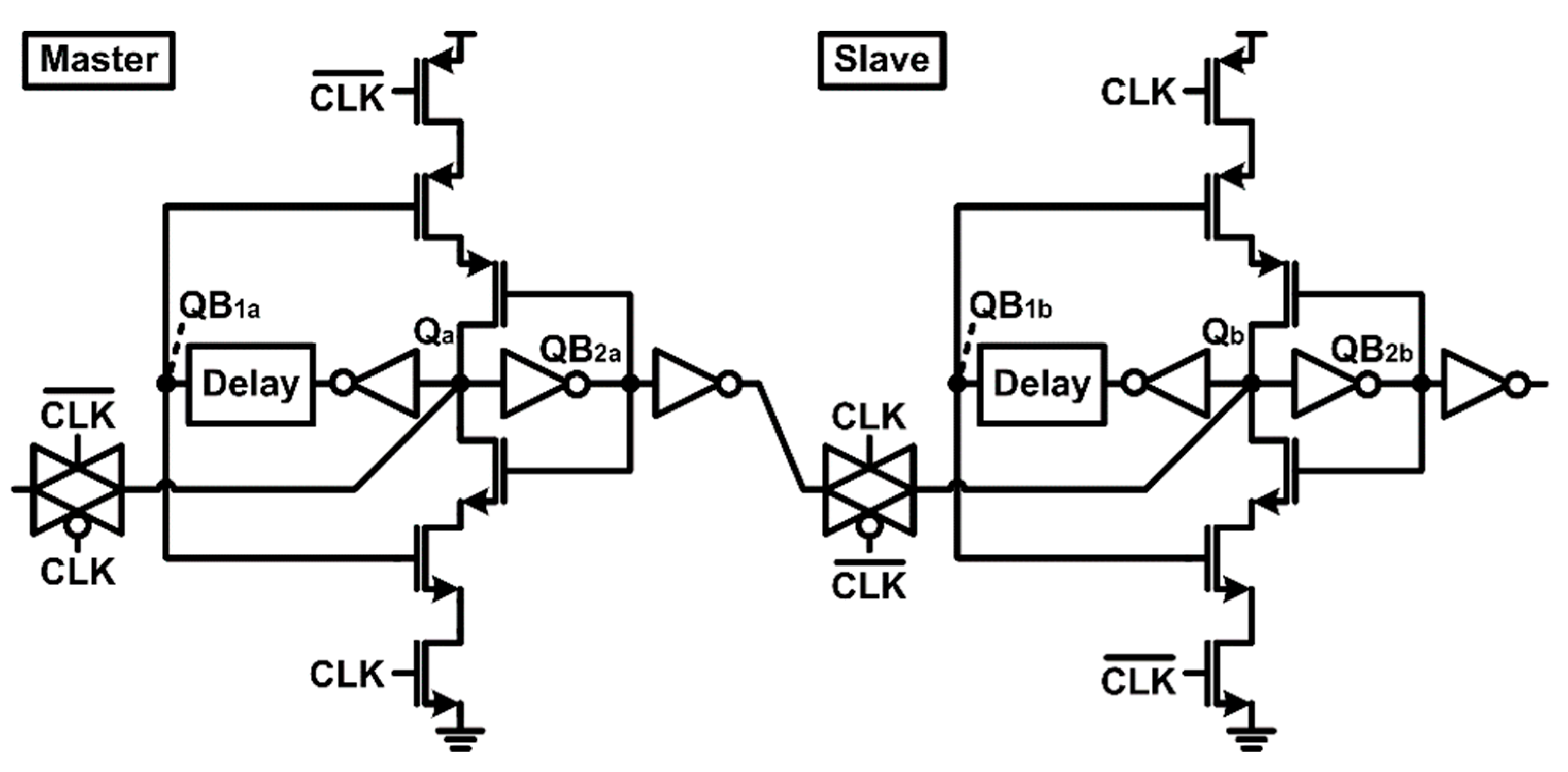
3.2. Proposed Radiation-Hardened Flip-Flop
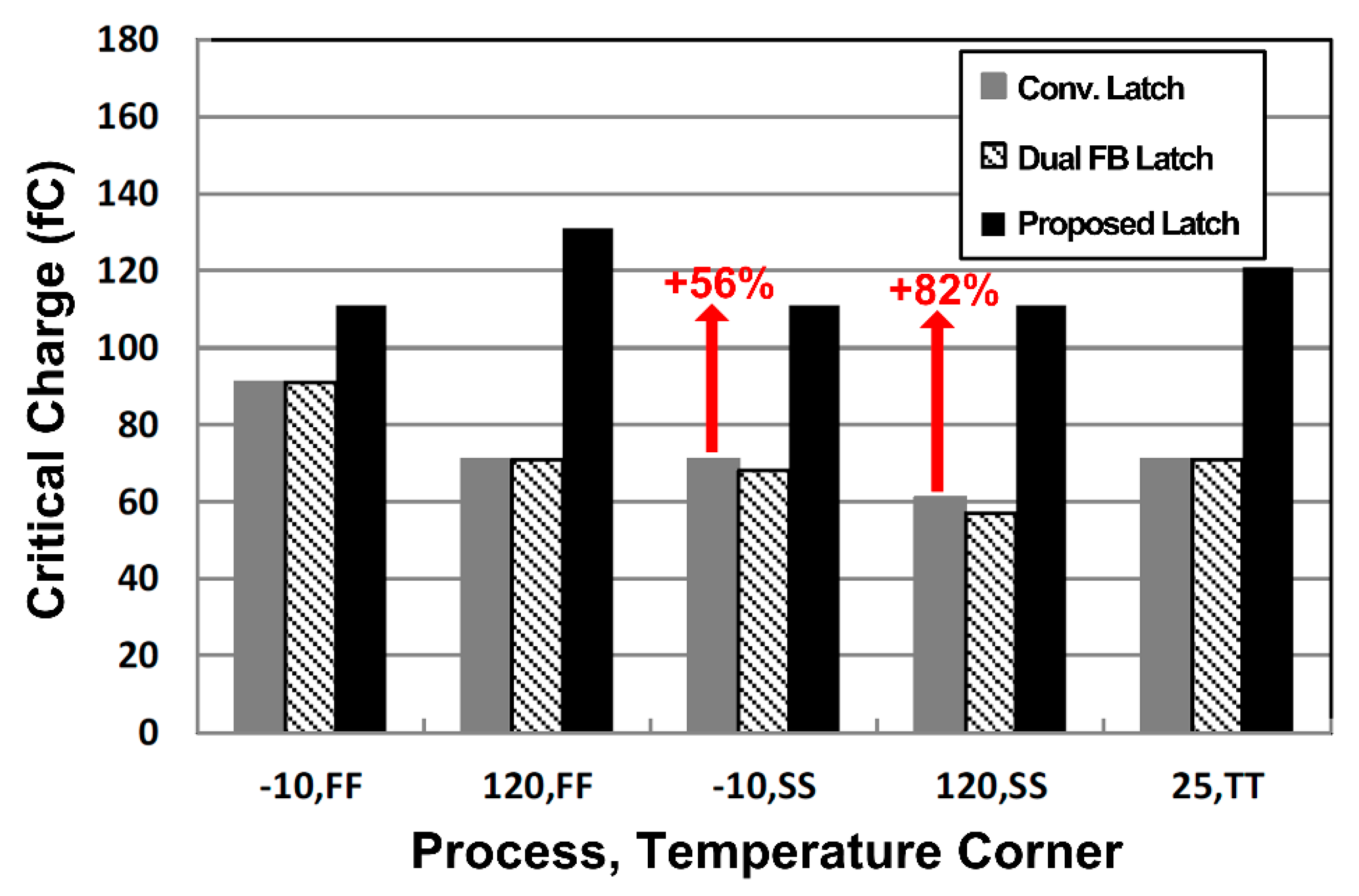
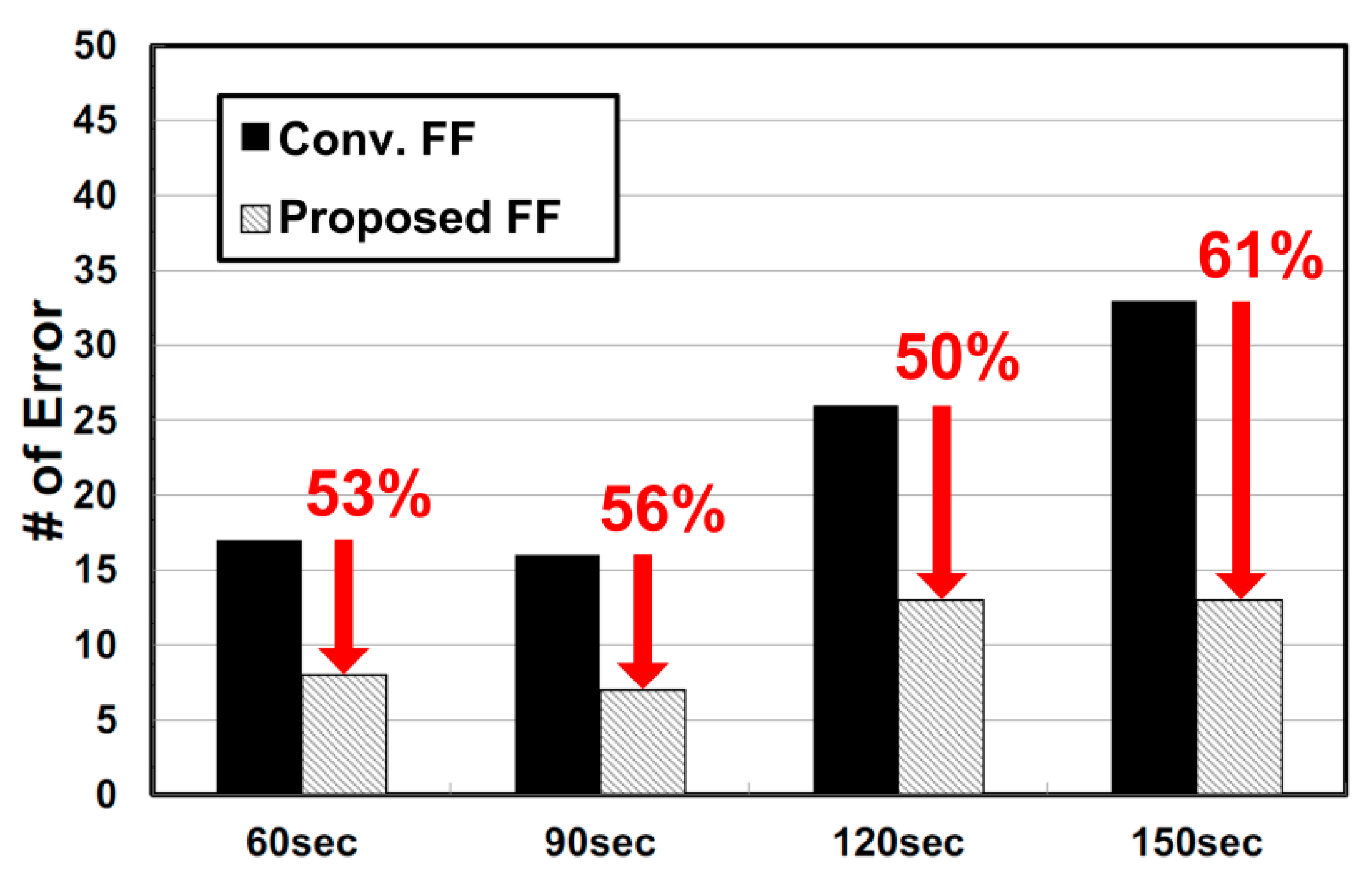
3.3. Radiation-Hardened Flip-Flop Comparison
4. Measurement Results
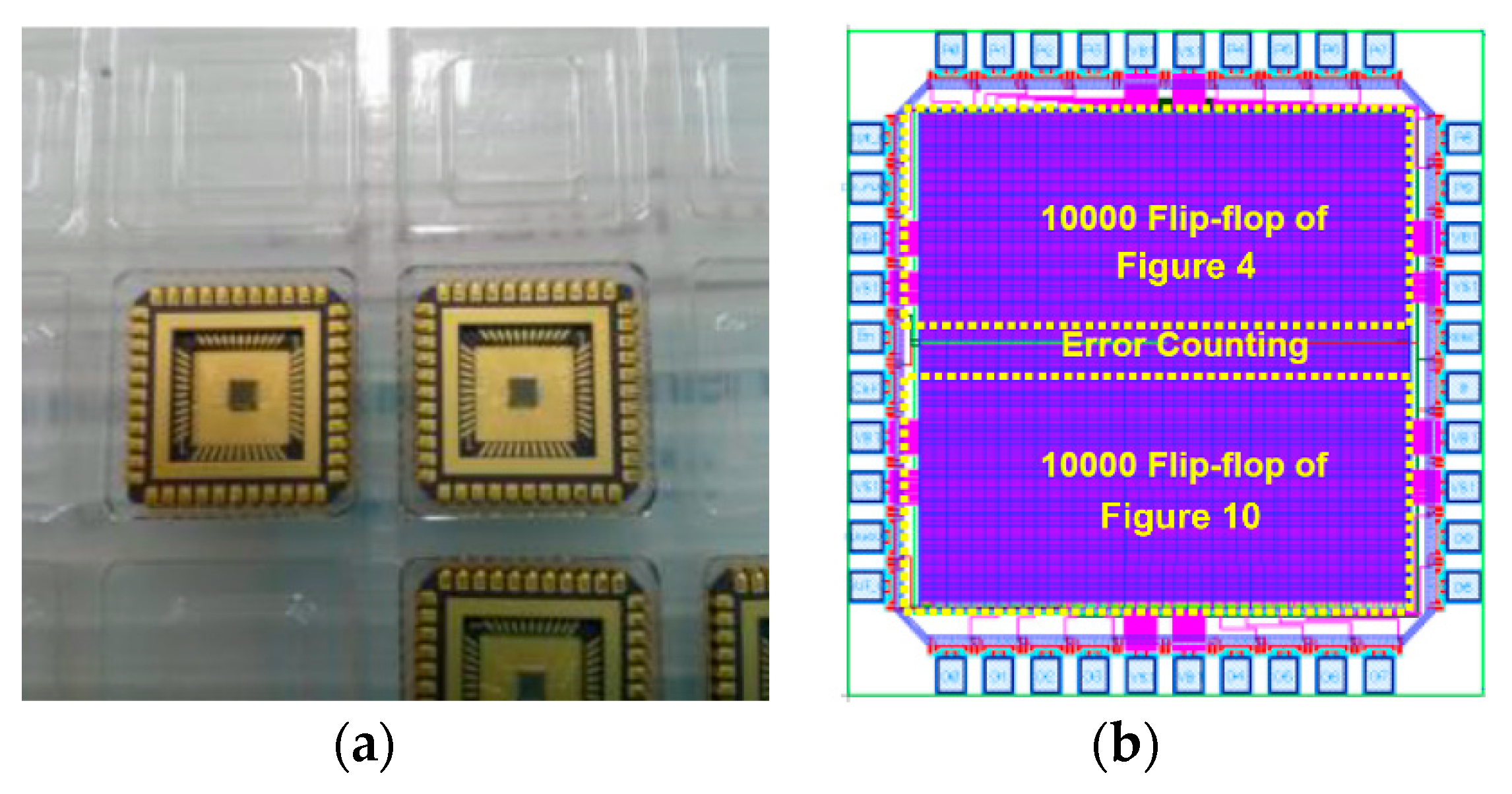
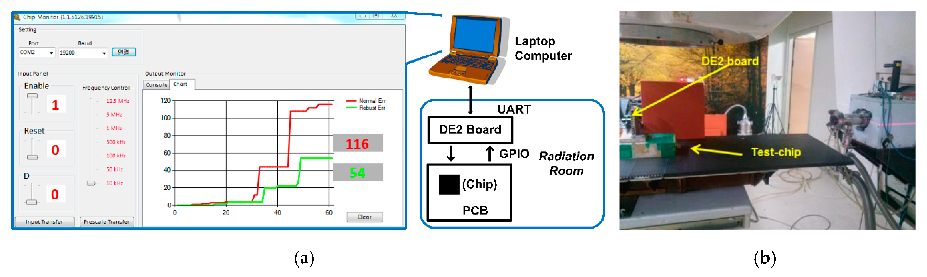
4.1. Test Chip Fabrication and Radiation Test Setup
4.2. Test Chip Verification in Radiation Environments
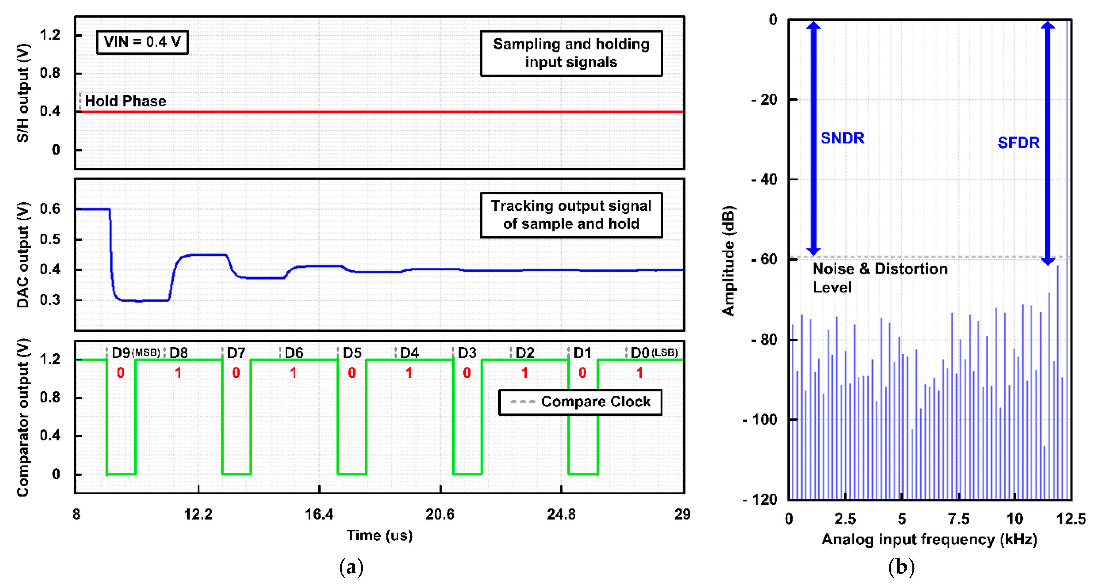
4.3. Verification of the Radiation-Hardened SAR ADC with the Proposed Flip-Flop
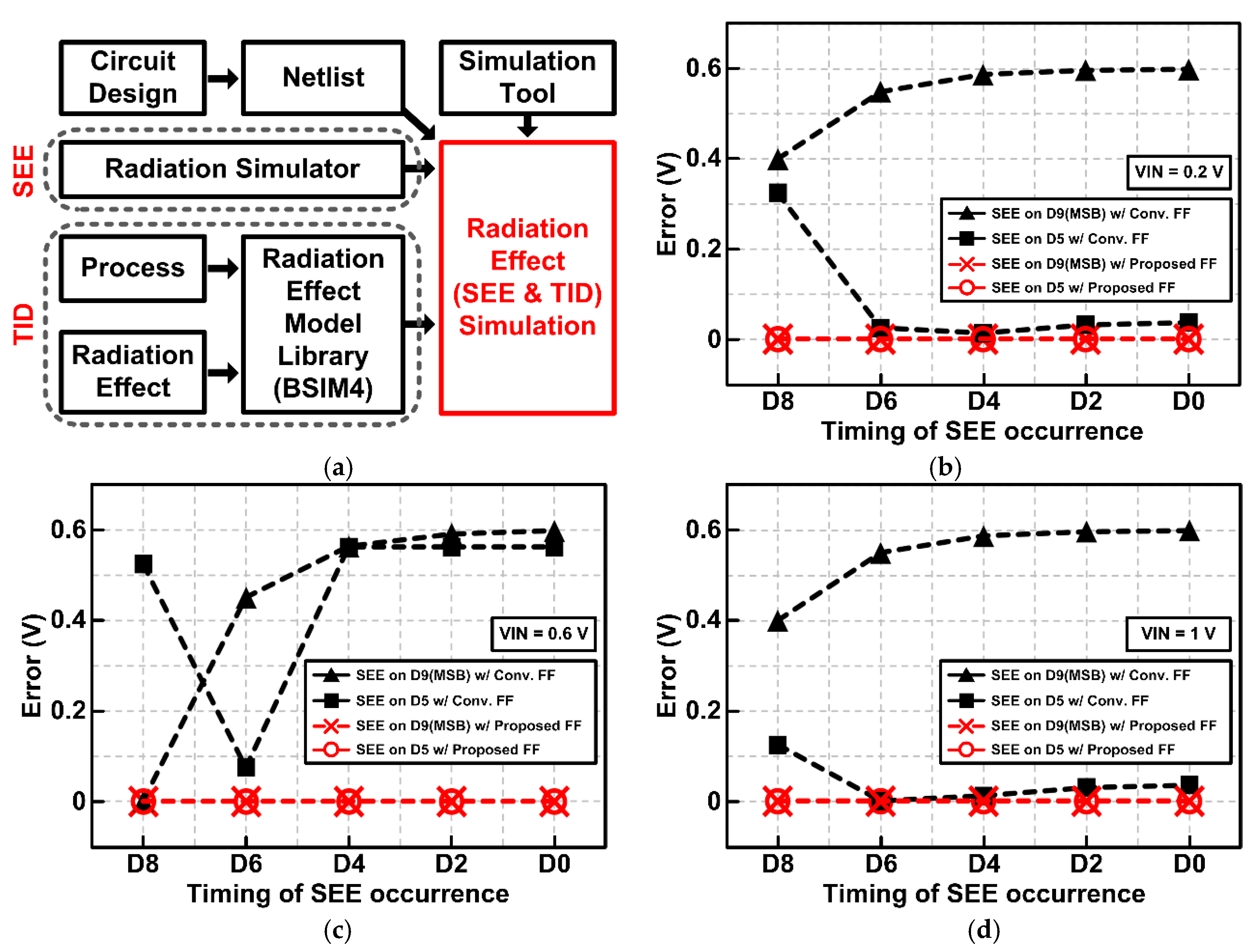
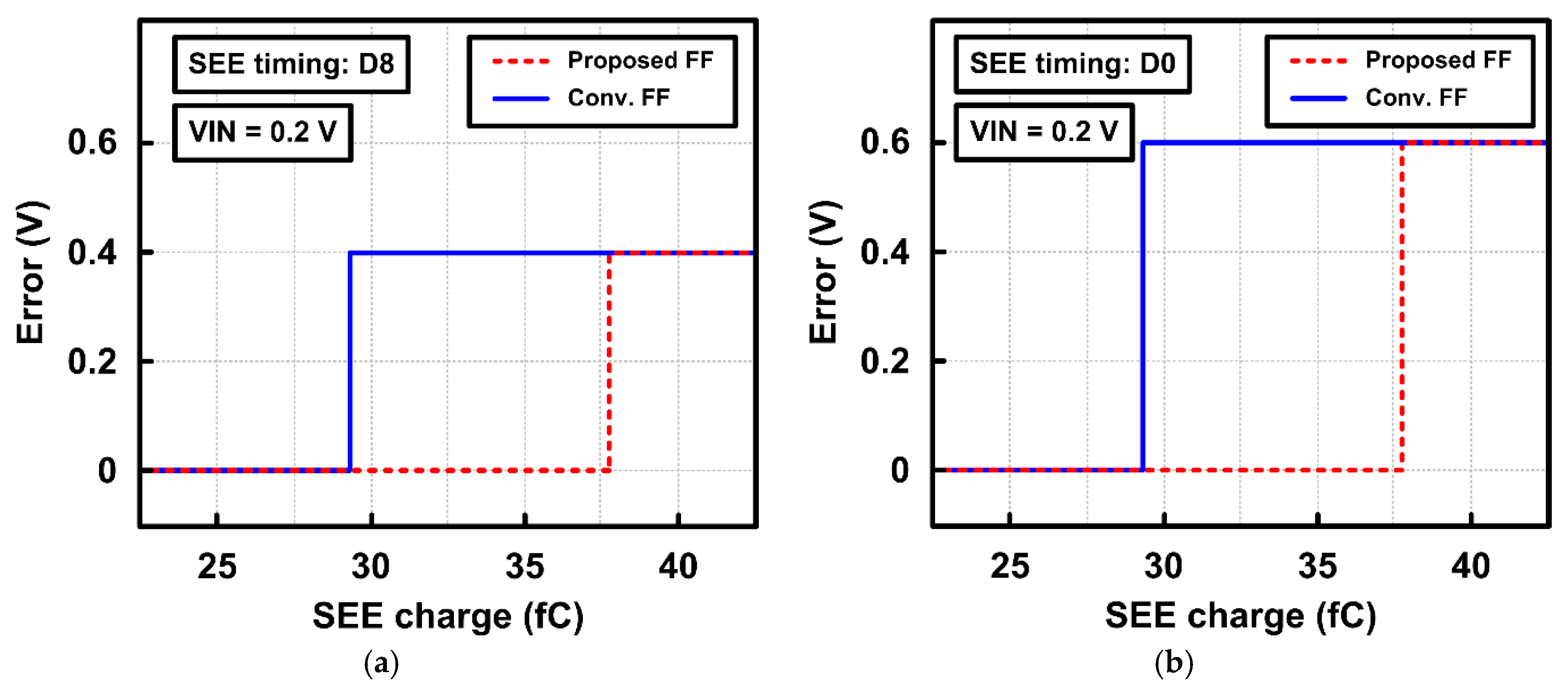
4.4. Radiation Tolerance of the Proposed Flip-Flop Against Both TID and SEE
5. Conclusions
Author Contributions
Funding
Acknowledgments
Conflicts of Interest
References
- Leroux, P.; Van Koeckhoven, W.; Verbeeck, J.; Van Uffelen, M.; Esqué, S.; Ranz, R.; Damiani, C.; Hamilton, D. Design of a MGy radiation tolerant resolver-to-digital convertor IC for remotely operated maintenance in harsh environments. Fusion Eng. Des. 2014, 89, 2314–2319. [Google Scholar] [CrossRef]
- Aal, A.; Polte, T. On component reliability and system reliability for automotive applications. In Proceedings of the 2012 IEEE International Integrated Reliability Workshop Final Report, South Lake Tahoe, CA, USA, 14–18 October 2012; pp. 168–170. [Google Scholar]
- Barnaby, H.J. Total-ionizing-dose effects in modern CMOS technologies. IEEE Trans. Nucl. Sci. 2006, 53, 3103–3121. [Google Scholar] [CrossRef]
- Turflinger, T.L. Single-event effects in analog and mixed-signal integrated circuits. IEEE Trans. Nucl. Sci. 1996, 43, 594–602. [Google Scholar] [CrossRef]
- Virmontois, C.; Goiffon, V.; Magnan, P.; Girard, S.; Inguimbert, C.; Petit, S.; Rolland, G.; Saint-Pé, O. Displacement damage effects due to neutron and proton irradiations on CMOS image sensors manufactured in deep submicron technology. IEEE Trans. Nucl. Sci. 2010, 57, 3101–3108. [Google Scholar] [CrossRef] [Green Version]
- Gatti, U.; Calligaro, C.; Pikhay, E.; Roizin, Y. Radiation-hardened techniques for CMOS flash ADC. In Proceedings of the IEEE International Conference on Electronics Circuits and Systems (ICECS), Marseille, France, 7–10 December 2014. [Google Scholar]
- Sternberg, A.L.; Massengill, L.W.; Hale, M.; Blalock, B. Single-Event Sensitivity and Hardening of a Pipelined Analog-to-Digital Converter. IEEE Trans. Nucl. Sci. 2006, 53, 3532–3538. [Google Scholar] [CrossRef]
- Verbeeck, J.; Van Uffelen, M.; Steyaert, M.; Leroux, P. 17 bit 4.35 mW 1 kHz delta sigma ADC and 256-to-1 multiplexer for remote handling instrumentation equipment. Fusion Eng. Des. 2013, 88, 1942–1946. [Google Scholar] [CrossRef]
- Baker, R.J. CMOS Circuit Design, Layout, and Simulation; Wiley: Hoboken, NJ, USA, 2010; pp. 985–1098. [Google Scholar]
- Baghbanmanesh, M.; Maloberti, F.; Gatti, U. A 10-Bit Radiation-Hardened by Design (RHBD) SAR ADC for Space Applications. In Proceedings of the 2017 New Generation of CAS (NGCAS), Genova, Italy, 6–8 September 2017; pp. 53–56. [Google Scholar]
- Jeong, K.; Ro, D.; Lee, G.; Kang, M.; Lee, H.-M. A Radiation-Hardened Instrumentation Amplifier for Sensor Readout Integrated Circuits in Nuclear Fusion Applications. Electronics 2018, 7, 429. [Google Scholar] [CrossRef] [Green Version]
- Dodd, P.E.; Massengill, L.W. Basic mechanisms and modeling of single-event upset in digital microelectronics. IEEE Trans. Nucl. Sci. 2003, 50, 583–602. [Google Scholar] [CrossRef]
- Dang, L.D.T.; Kim, J.S.; Chang, I.J. We-Quatro: Radiaiton-hardened SRAM cell with parametric process variation tolerance. IEEE Trans. Nucl. Sci. 2017, 64, 2489–2496. [Google Scholar] [CrossRef]
- Omana, M.; Rossi, D.; Metra, C. Latch Susceptibility to Transient Faults and New Hardening Approach. IEEE Trans. Comput. 2007, 56, 1255–1268. [Google Scholar] [CrossRef]
- Naseer, R.; Boulghassoul, Y.; Draper, J.; DasGupta, S.; Witulski, A. Critical Charge Characterization for Soft Error Rate Modeling in 90nm SRAM. In Proceedings of the IEEE International Symposium on Circuits and Systems, New Orleans, LA, USA, 27–30 May 2007; pp. 1879–1882. [Google Scholar]
- Messenger, G.; Milton, M. Single Event Phenomena; Chapman & Hall: London, UK, 1997. [Google Scholar]
- Kang, M.; Park, I.H.; Chang, I.J.; Lee, K.; Seo, S.; Park, B.-G.; Shin, H. An accurate compact model considering direct-channel interference of adjacent cells in sub-30-nm NAND flash technologies. IEEE Electron Device Lett. 2012, 33, 1114–1116. [Google Scholar] [CrossRef]


| ADC Structure | Flash | Pipelined | Sigma-Delta | SAR |
|---|---|---|---|---|
| High Resolution | X | O | O | O |
| High Sampling Rate | O | O | X | Δ |
| TID Tolerance | X | X | X | O |
| SEE Tolerance | O | O | Δ | Δ |
| Flip-Flop | Conventional | DICE | Quatro | This Work |
|---|---|---|---|---|
| Power (norm.) | 1 | 1.9 | 2.0 | 1.2 |
| Area (norm.) | 1 | 1.8 | 2.1 | 1.3 |
| C-Q Delay (norm.) | 1 | 1.85 | 1.42 | 1.41 |
| D-Q Delay (norm.) | 1 | 1.8 | 1.43 | 1.4 |
| SEE Tolerance | X | O | O | O |
| Specification (Unit) | Simulation Results |
|---|---|
| Architecture | SAR |
| Technology (nm) | 65 |
| Supply Voltage (V) | 1.2 |
| Input Range (Vp-p) | 1.2 |
| Sampling Rate (kS/s) | 25 |
| Resolution (bit) | 10 |
| SNR (dB) | 62.43 |
| THD (dB) | -62.3 |
| SNDR (dB) | 59.49 |
| SFDR (dB) | 63.13 |
| ENOB (bit) | 9.59 |
| Power (mW) | 0.84 |
© 2019 by the authors. Licensee MDPI, Basel, Switzerland. This article is an open access article distributed under the terms and conditions of the Creative Commons Attribution (CC BY) license (http://creativecommons.org/licenses/by/4.0/).
Share and Cite
Ro, D.; Min, C.; Kang, M.; Chang, I.J.; Lee, H.-M. A Radiation-Hardened SAR ADC with Delay-Based Dual Feedback Flip-Flops for Sensor Readout Systems. Sensors 2020, 20, 171. https://doi.org/10.3390/s20010171
Ro D, Min C, Kang M, Chang IJ, Lee H-M. A Radiation-Hardened SAR ADC with Delay-Based Dual Feedback Flip-Flops for Sensor Readout Systems. Sensors. 2020; 20(1):171. https://doi.org/10.3390/s20010171
Chicago/Turabian StyleRo, Duckhoon, Changhong Min, Myounggon Kang, Ik Joon Chang, and Hyung-Min Lee. 2020. "A Radiation-Hardened SAR ADC with Delay-Based Dual Feedback Flip-Flops for Sensor Readout Systems" Sensors 20, no. 1: 171. https://doi.org/10.3390/s20010171