Abstract
A dual-frequency all-in-one Global Navigation Satellite System (GNSS) receiver with a multi-core 32-bit RISC (reduced instruction set computing) application processor was integrated and manufactured as a System-on-Chip (SoC) in a 110 nm CMOS (complementary metal-oxide semiconductor) process. The GNSS RF (radio frequency) front-end with baseband navigation engine is able to receive, simultaneously, Galileo (European Global Satellite Navigation System) E1/E5ab, GPS (US Global Positioning System) L1/L1C/L5, BeiDou (Chinese Navigation Satellite System) B1/B2, GLONASS (GLObal NAvigation Satellite System of Russian Government) L1/L3/L5, QZSS (Quasi-Zenith Satellite System development by the Japanese government) L1/L5 and IRNSS (Indian Regional Navigation Satellite System) L5, as well as all SBAS (Satellite Based Augmentation System) signals. The ability of the GNSS to detect such a broad range of signals allows for high-accuracy positioning. The whole SoC (system-on-chip), which is connected to a small passive antenna, provides precise position, velocity and time or raw GNSS data for hybridization with the IMU (inertial measurement unit) without the need for an external application processor. Additionally, user application can be executed directly in the SoC. It works in the −40 to +105 °C temperature range with a 1.5 V supply. The assembled test-chip takes 100 pins in a QFN (quad-flat no-leads) package and needs only a quartz crystal for the on-chip reference clock driver and optional SAW (surface acoustic wave) filters. The radio performance for both wideband (52 MHz) channels centered at L1/E1 and L5/E5 is NF = 2.3 dB, G = 131 dB, with 121 dBc/Hz of phase noise @ 1 MHz offset from the carrier, consumes 35 mW and occupies a 4.5 mm2 silicon area. The SoC reported in the paper is the first ever dual-frequency single-chip GNSS receiver equipped with a multi-core application microcontroller integrated with embedded flash memory for the user application program.
1. Introduction
The global GNSS (Global Navigation Satellite System) market has been growing continuously over recent years [1,2]. Applications relying on GNSS positioning have become a part of everyday life, leading to an increased variety of Location-Based Services (LBS). Nowadays, the LBS consumer market is dominated by single frequency (typically L1/E1 band), low cost and highly integrated GNSS receivers [3,4,5,6,7,8,9]. The use of such receivers comes with two main limitations: low precision and low reliability. Additionally, limitations such as: signal availability in challenging environments (such as urban canyons) and susceptibility to multipath, interference, jamming and spoofing further obstruct the penetration of the LBS segment by GNSS. Such hurdles are typically overcome by employing multi-constellation, multi-frequency receivers which use additional complementary positioning technologies (i.e., inertial measurement unit (IMU)) when necessary [10].
The positioning precision of single-frequency receivers is substantially affected by the ionospheric delay effect. Although different models (e.g., Klobuchar, NeQiock-G) are used to compensate for this effect, the resulting error is estimated as 7 m RMS (root mean square) [11]. As the ionospheric delay depends on the signal frequency, the so-called ionospheric free combination may be used in dual frequency receivers to reduce the positioning error related to the residual ionospheric delay down to 0.1 m RMS [11]. Another issue associated with positioning precision is due to the multipath effect, which is especially important in urban canyons. There are methods to reduce the impact of this effect and here, the use of multi-constellation GNSS provides substantial improvements [12].
The positioning reliability is also improved when using a multi-frequency multi-constellation receiver. It is especially visible in urban environments, where signals can be shadowed by high buildings. Having access to a higher number of satellites reduces the probability that the number of visible satellites will drop down to a level which makes positioning impossible This receiver is also more robust against spoofing, as spoofing devices need to generate replicas of all signals tracked by the device.
The above techniques are available only in professional high-precision and reliable navigation solutions, which are large in size, have a high power consumption and come at a high price. The existing consumer and professional GNSS equipment, which is usually small in size and comes at a low cost, is not suitable for many LBS applications that need reliable and precise (better than 1 m) positioning.
To overcome the limitations mentioned above, extensive research on the CMOS (complementary metal-oxide semiconductor) integration of the dual-frequency radio frequency (RF) front-end for GNSS has been performed [13,14,15,16,17,18,19]. So far, most of the designs either offer only configurability between different bands of GNSS without the possibility of simultaneous multi-frequency reception of all constellations by a single chip [13,15,16,19] or they do not receive all bands from the most popular GNSS systems and focus only on L1/E1 and L5/E5a reception [14,17].
This paper presents the design of the CCNV1-A1 chip developed under the NaviSoC project [20], the first ever dual-frequency, multi-band, multi-constellation navigation receiver integrated with a multi-core application microprocessor as one SoC (System-on-a-Chip) capable of receiving, simultaneously, all GNSS signals located in L1/E1 and L5/E5 bands. The scope of the paper covers hardware description and results. The main focus is on the noise, gain and bandwidth of the designed system, as these are the main parameters that can influence the overall system performance. The overall navigation system is not fully covered. The receiver parameters, such as sensitivity, strongly depend on the signal type received and demodulation algorithms. The algorithms are a part of navigational software which is currently under development. For that reason, some system level parameters are not presented.
The paper is organized as follows. Section 2 provides an overview of the SoC, application processor unit and frequency plan with radio architecture. The circuit level design is described in Section 3. A comparison with state-of-the-art parameters is reported in Section 4. The paper ends with a conclusion.
2. SoC Overview and RF Architecture
2.1. SoC Overview
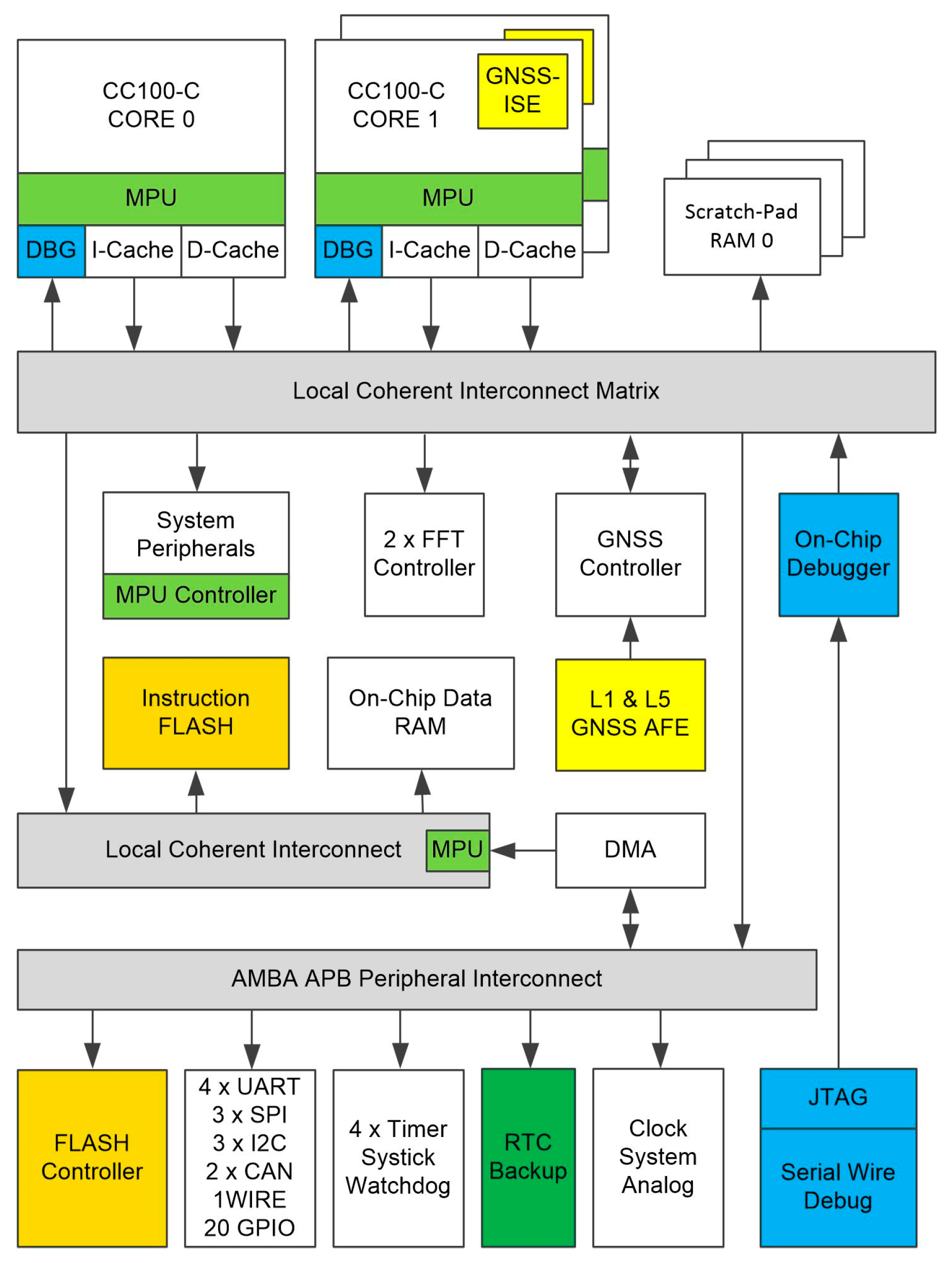
An overview of the CCNV1-A1 chip is shown in Figure 1. The chip consists of a three-core microcontroller featuring a rich set of peripherals, a 512 kiB SRAM (static random-access memory) and a 768 kiB eFlash.

Figure 1.
Block diagram of the CCNV1-A1 GNSS receiver system-on-chip (SoC).
The peripherals associated with the GNSS receiver include two 256-point FFT (fast Fourier transform) cores, as well as a dedicated module supporting signal acquisition (see Figure 1; GNSS Controller). The microcontroller peripherals include a number of communications interfaces (UARTs, SPIs, I2C, CAN, 1WIRE) and GPIO (general-purpose input/output), as well as timers, a watchdog and a battery backed-up RTC (real-time clock) domain. Two out of the three cores support the instruction set extension (GNSS-ISE [21]) for GNSS signal processing. GNSS-ISE forms two autonomous 16-channel GNSS baseband coprocessors. The third core is intended for user application. The required external components are a passive antenna, a crystal oscillator, a few capacitances which decouple supply and optionally external SAW (surface acoustic wave) filters.
2.2. Radio Architecture for GNSS Signals
A detailed block diagram of the GNSS radio is shown in Figure 2. It is divided into three main modules:
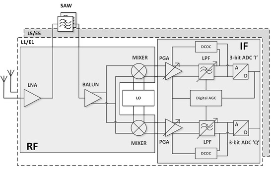
Figure 2.
Block diagram of the dual-frequency GNSS AFE radio block.
- RF circuits that amplify and filter the GNSS signals received from an external passive antenna and pass them to the mixers,
- An LO (local oscillator) generation module implemented as an ADPLL (all-digital phase-locked loop),
- IF (intermediate frequency) blocks (programmable gain amplifier (PGA), low pass filter (LPF), automatic gain control (AGC)) that process low-frequency I/Q (in-phase and quadrature) signals for 3-bit complex analog-to-digital converters (ADC).
This approach allows complex processing to be moved to the digital domain, making the receiver more flexible. The GNSS AFE (analog front-end) was used to receive either any single GNSS signal or all GNSS signals centered around L1/E1 and L5/E5 bands simultaneously (see Figure 3).
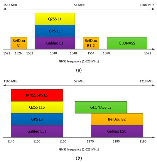
Figure 3.
GNSS signals received and processed by the CCNV1-A1 chip: (a) L1/E1 band, (b) L5/E5 band.
2.3. Frequency Planning for Dual-Frequency Receiver
The continuous expansion of the GNSS space segment leads to an increase in the number of navigational systems and signals available [22]. Because of that, choosing the appropriate frequency bands for dual-frequency receivers has been an important task. Bands centered around 1575.42 MHz (E1/L1 band of Galileo (European Global Satellite Navigation System) and GPS (US Global Positioning System)) and 1191.795 MHz (Galileo and GPS E5/L5 band) frequencies were chosen after a detailed analysis of the GNSS signals. The GNSS frequency spectrum depicted in Figure 3 clearly suggests that these bands allow all global and regional GNSS constellations to be received. In this case, setting the receiver bandwidth to 52 MHz allows for the reception of signals from all global systems—Galileo, GPS, BeiDou (Chinese Navigation Satellite System) and GLONASS (GLObal NAvigation Satellite System of Russian government), as well as local systems such as QZSS (Quasi-Zenith Satellite System developed by the Japanese government) and IRNSS (Indian Regional Navigation Satellite System). To reduce power consumption, the wideband RF processing is performed using a direct conversion receiver with complex signal processing. Consequently, the IF bandwidth and sampling frequency may be limited to 26 MHz and 64 MHz, respectively. As a result, a high positioning accuracy is achieved while the power is kept at a reasonable level.
Both channels’ bandwidth and sampling frequency are highly configurable. Therefore, the best accuracy/power ratio may be selected for any given application. This is a unique feature allowing the use of CCNV1-A1 in a wide range of applications. The sampling frequency can be changed from 8 MHz to 64 MHz. The channel bandwidth is automatically set to a frequency close to the Nyquist frequency.
3. Circuit Implementation
3.1. Low-Noise Amplifier
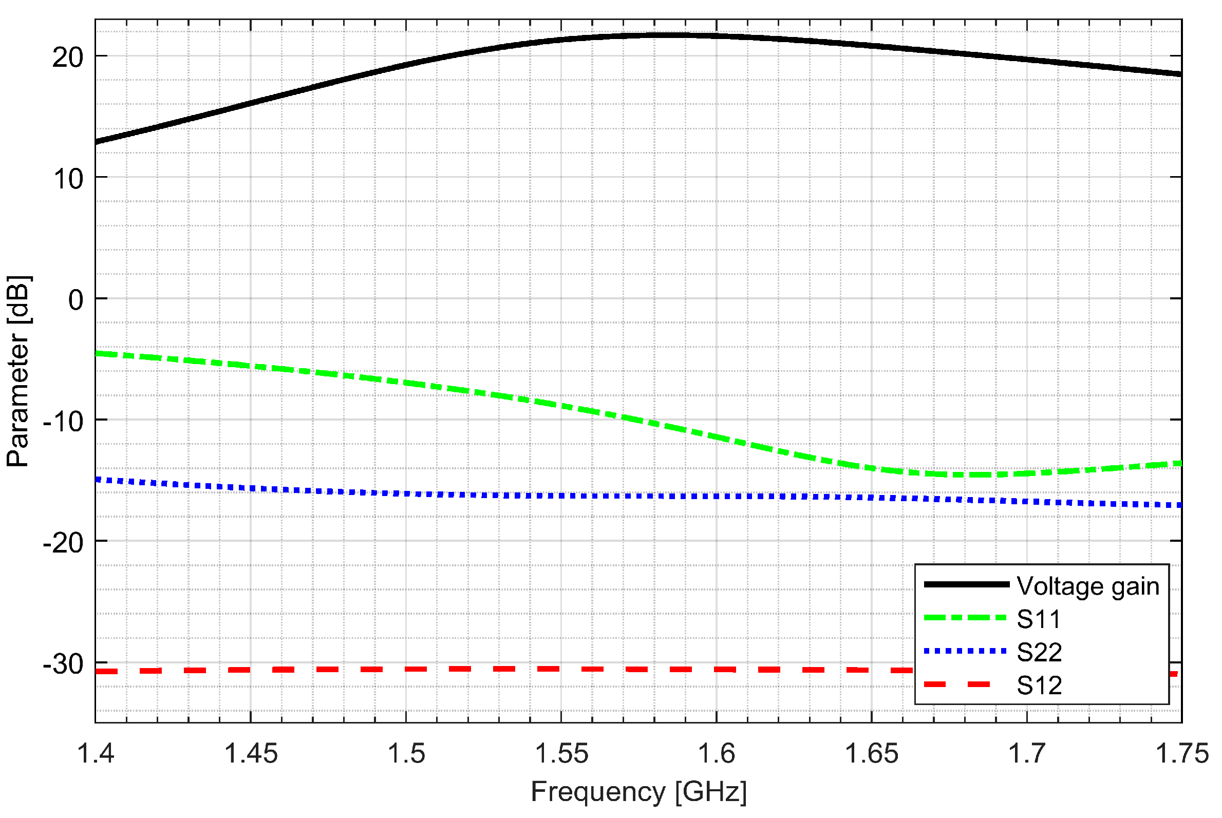
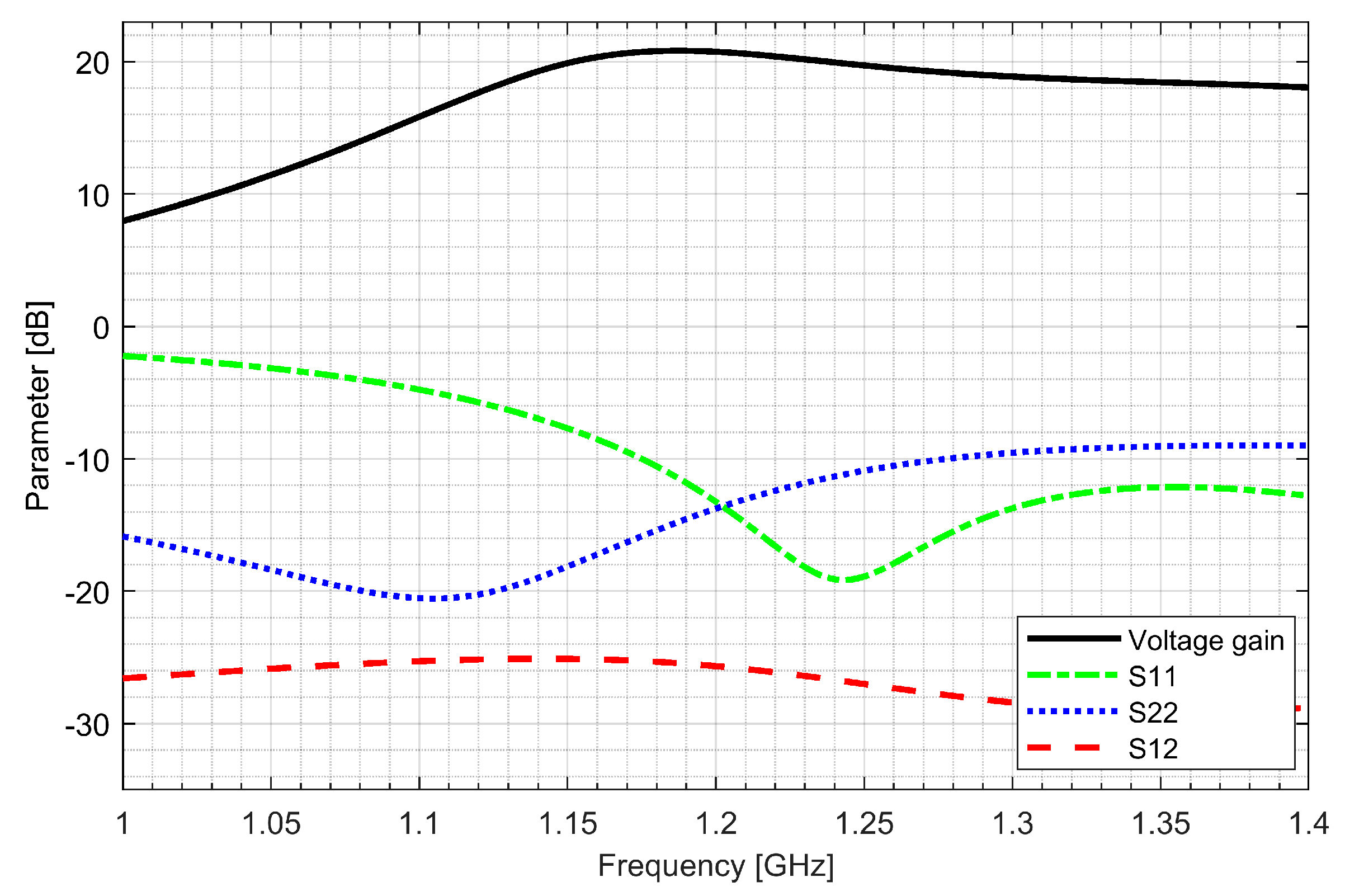
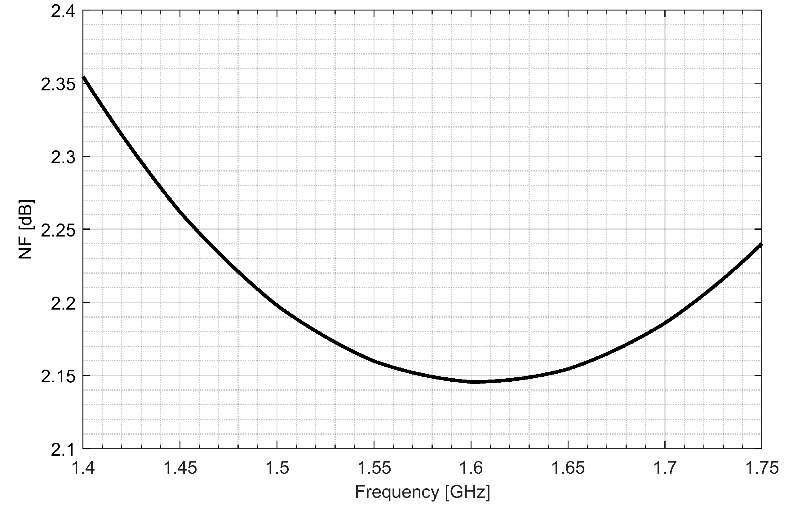
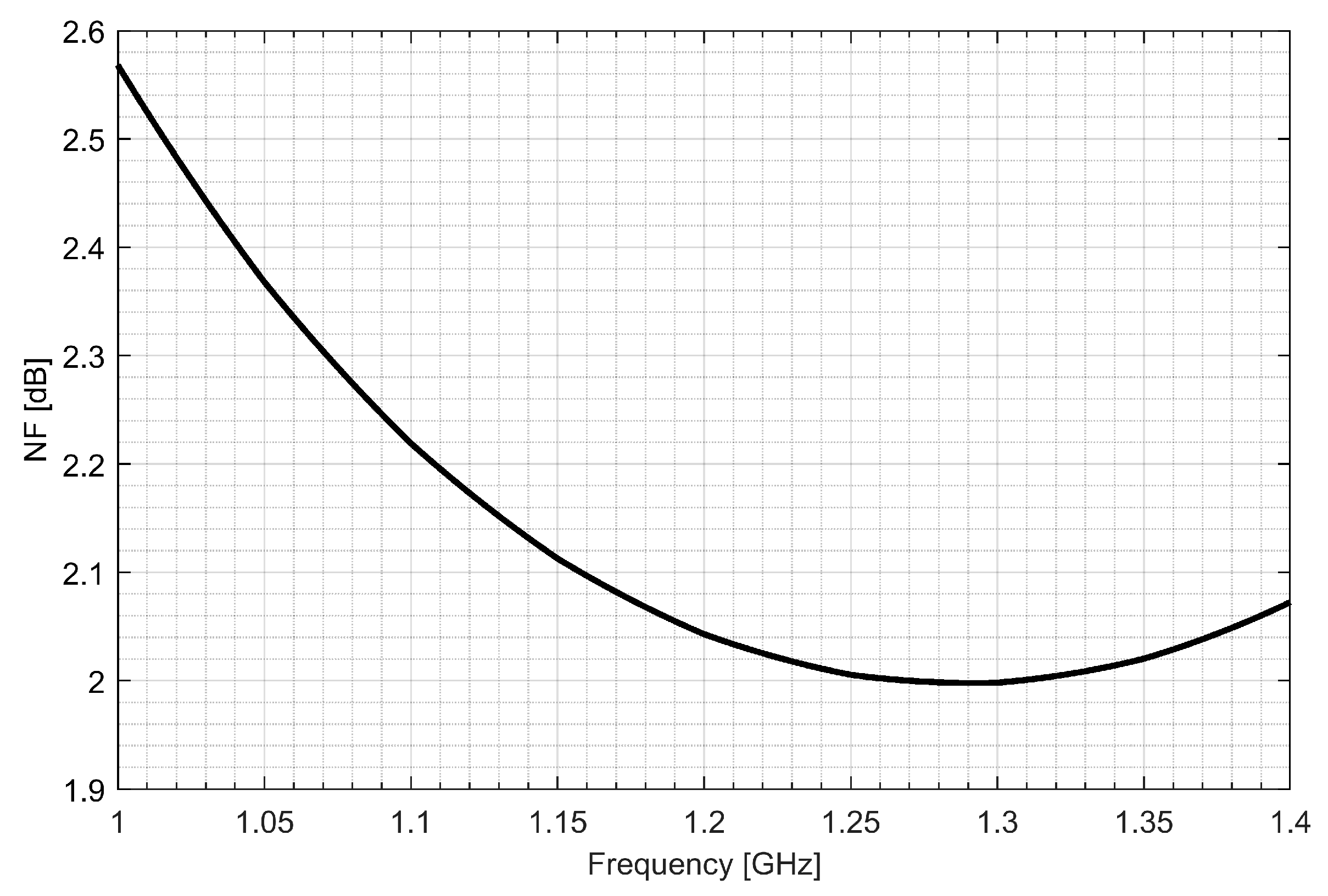
Two separate low-noise amplifiers (LNAs) for L1/E1 and L5/E5 bands were designed. LNAs were implemented as classic single-ended cascode amplifiers with inductive source degeneration. For better amplification and better matching of the output impedance, a source follower with an “L” matching network was used at the outputs of the LNAs. Additionally, a band calibration circuit was implemented as a bank of detachable capacitors, connected in parallel to the output LC load of the amplifiers. Figure 4 and Figure 5 show the post-layout simulation results for the S-matrix and the voltage gain of the L1/E1 and the L5/E5 LNA, respectively. The L1/E1 and the L5/E5 LNA noise figure (NF) characteristics are presented in Figure 6 and Figure 7, respectively. The parameters of the L1/E1 LNA are: NF = 2.2 dB, GV = 21.7 dB, S11 = −10.2 dB, S22 = −16.3 dB and IDD = 2.4 mA. The parameters of the L5/E5 LNA are: NF = 2.1 dB, GV = 20.8 dB, S11 = −12.0 dB, S22 = −14.6 dB and IDD = 2.3 mA.
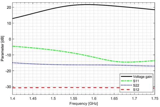
Figure 4.
S-matrix and voltage gain characteristics of the L1/E1 low-noise amplifier.
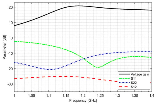
Figure 5.
S-matrix and voltage gain characteristics of the L5/E5 low-noise amplifier.
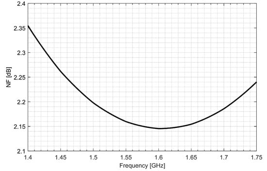
Figure 6.
Noise figure characteristics of the L1/E1 low-noise amplifier.

Figure 7.
Noise figure characteristics of the L5/E5 low-noise amplifier.
3.2. Active Balun and Down-Conversion Mixer
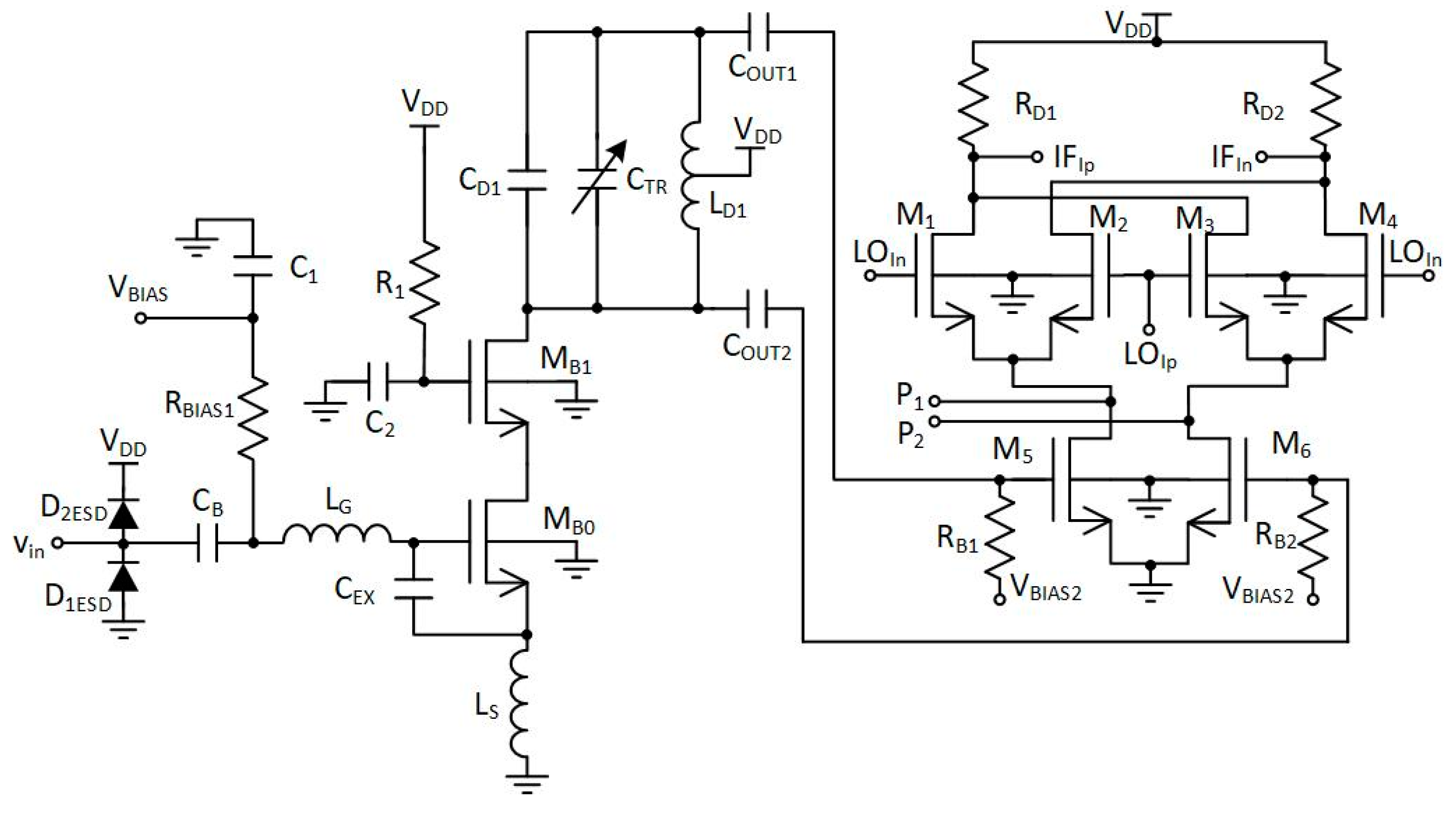
Figure 8 shows an active balun with ESD (electrostatic discharge) protection structures and a simplified active down-conversion mixer. For clarity, only the in-phase part of the quadrature mixer is shown in Figure 8. The quadrature part of the mixer was connected to ports P1 and P2.
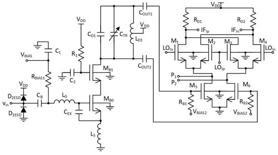
Figure 8.
Active balun with ESD (electrostatic discharge) protection and a simplified in-phase mixer.
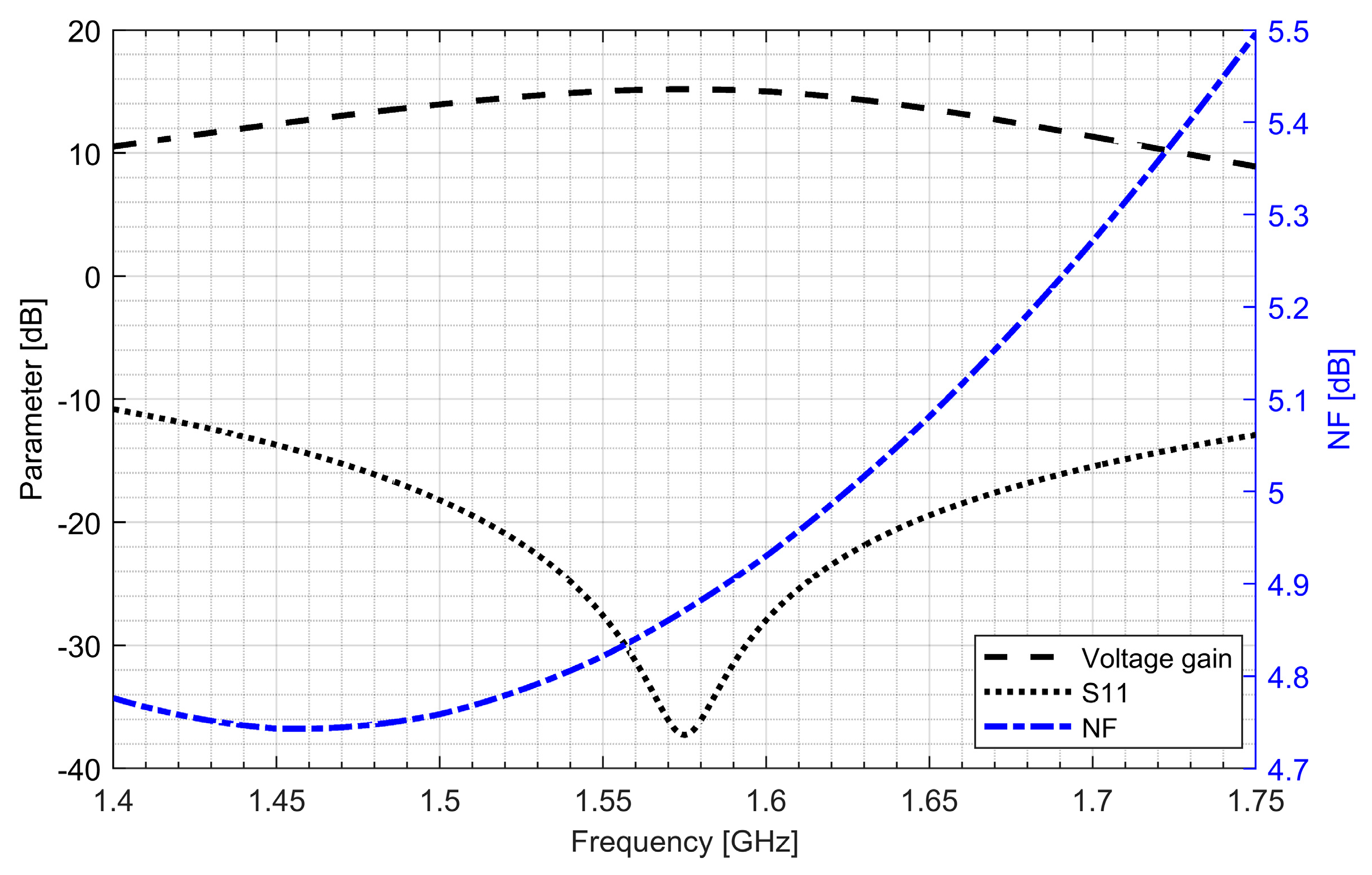
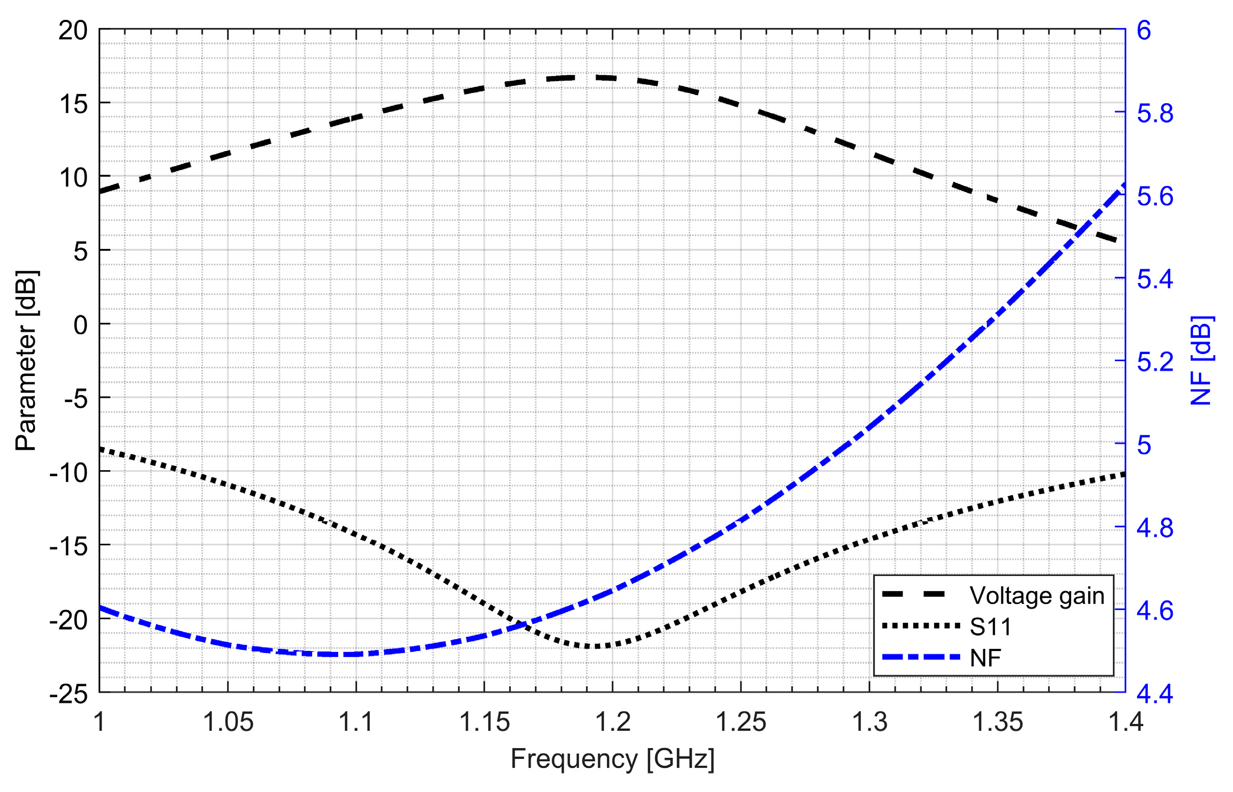
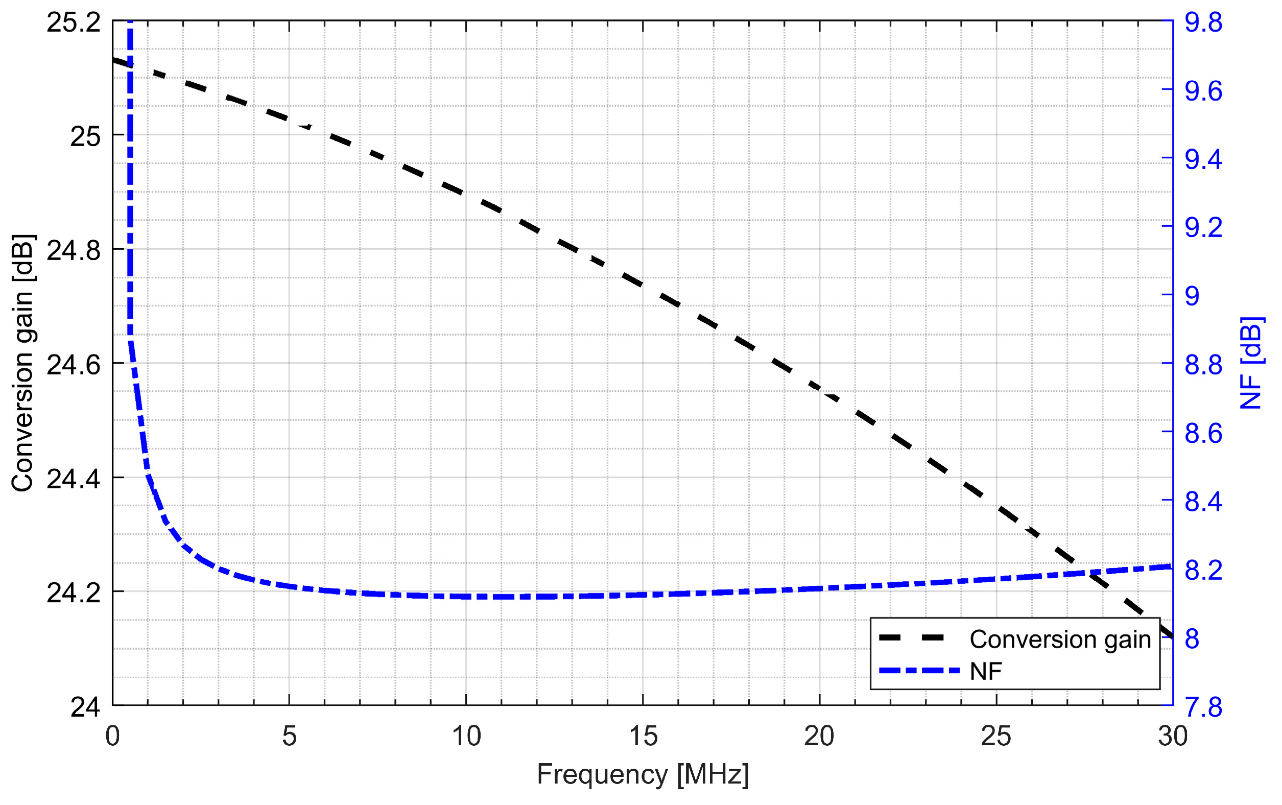
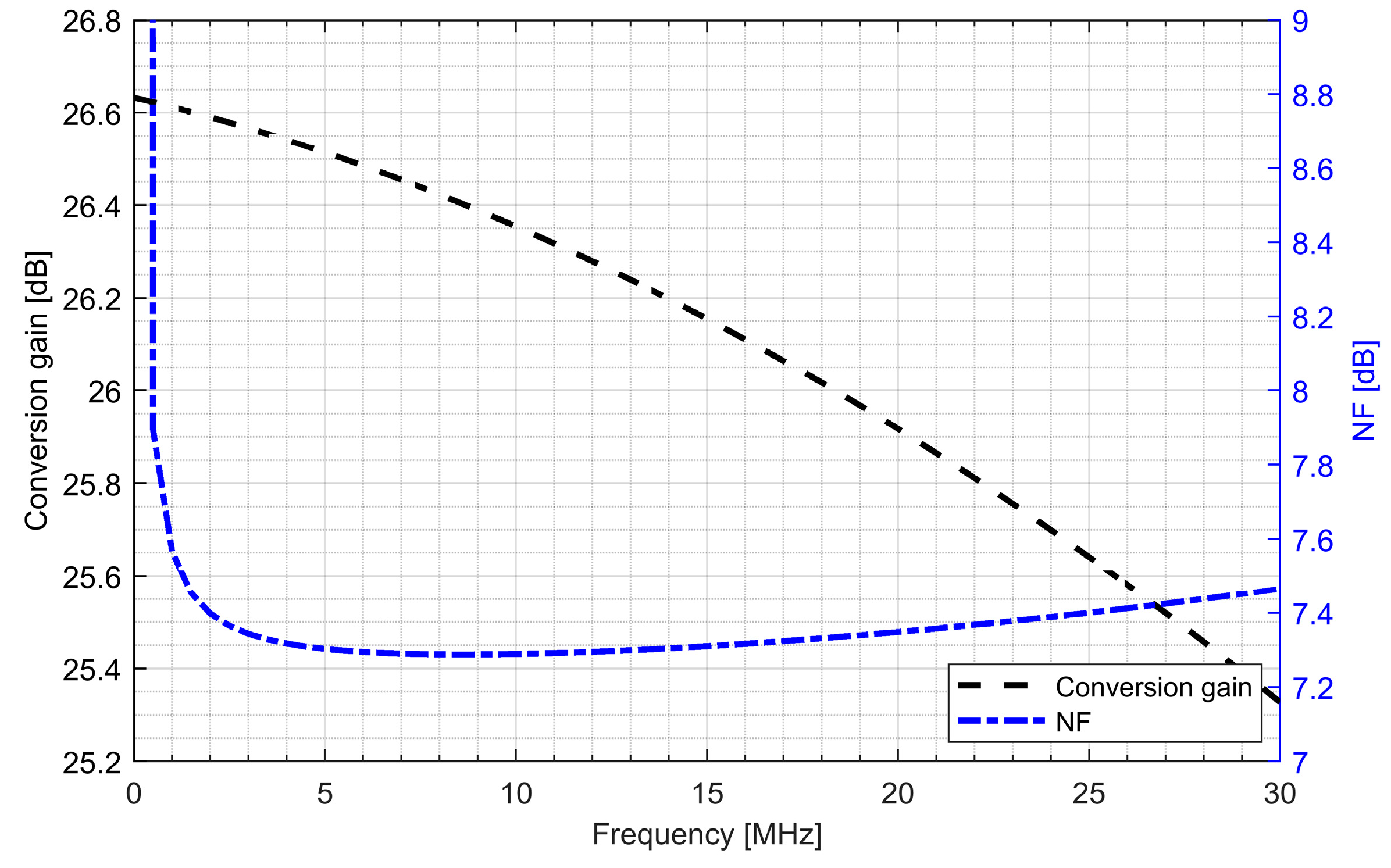
Active baluns (for L1/E1 and L5/E5 bands) perform triple functionality in GNSS AFE. They ensure a 50 Ω input matching, provide additional signal amplification and supply a differential RF signal to the down-conversion mixer. By using a center-tapped differential inductor to generate a differential signal at the output of the balun, the phase shift reaches 180° with high accuracy and the gain at each output is almost identical. The simulated PVT (process, voltage and temperature) variations of the phase and gain variation between outputs do not exceed 5° and 1 dB, respectively. The use of active baluns made it possible to reduce the noise requirements of the mixers. Figure 9; Figure 10 show the post-layout simulation results for the reflection coefficient (S11), voltage gain and noise figure of the L1/E1 and the L5/E5 balun, respectively. The L1/E1 and L5/E5 noise figure and the mixer conversion gain for the balun and mixer combined are presented in Figure 11 and Figure 12, respectively. The parameters of the L1/E1 balun are: NF = 4.9 dB, GV = 15.1 dB, S11 = −37.3 dB and IDD = 0.54 mA. The parameters of the L5/E5 balun are: NF = 4.6 dB, GV = 16.7 dB, S11 = −21.9 dB and IDD = 0.64 mA. The parameters of the mixer for L1/E1 band are: NF = 15.5 dB, GMIX = 10.4 dB and IDD = 0.48 mA. The parameters of the mixer for the L5/E5 band are: NF = 15.2 dB, GMIX = 10.3 dB and IDD = 0.48 mA. The combined parameters for the L1/E1 band are: NF = 8.2 dB, GCONV = 25.0 dB and IDD = 1.02 mA. The combined parameters for the L5/E5 band are: NF = 7.3 dB, GCONV = 26.5 dB and IDD = 1.12 mA.
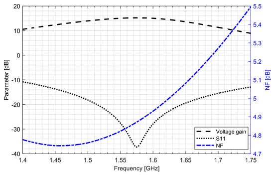
Figure 9.
S11, voltage gain and noise figure characteristics of the L1/E1 band active balun.
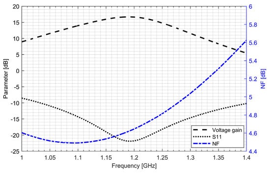
Figure 10.
S11, voltage gain and noise figure characteristics of the L5/E5 band active balun.
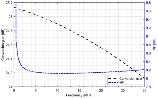
Figure 11.
Conversion gain and noise figure characteristics of the L1/E1 band active balun and mixer.
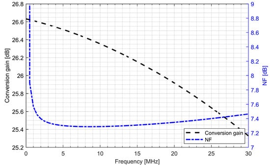
Figure 12.
Conversion gain and noise figure characteristics of the L5/E5 band active balun and mixer.
3.3. Radio-Frequency Front-End
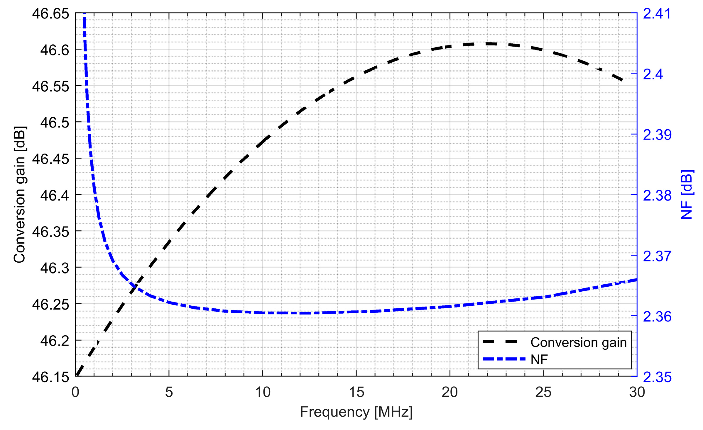
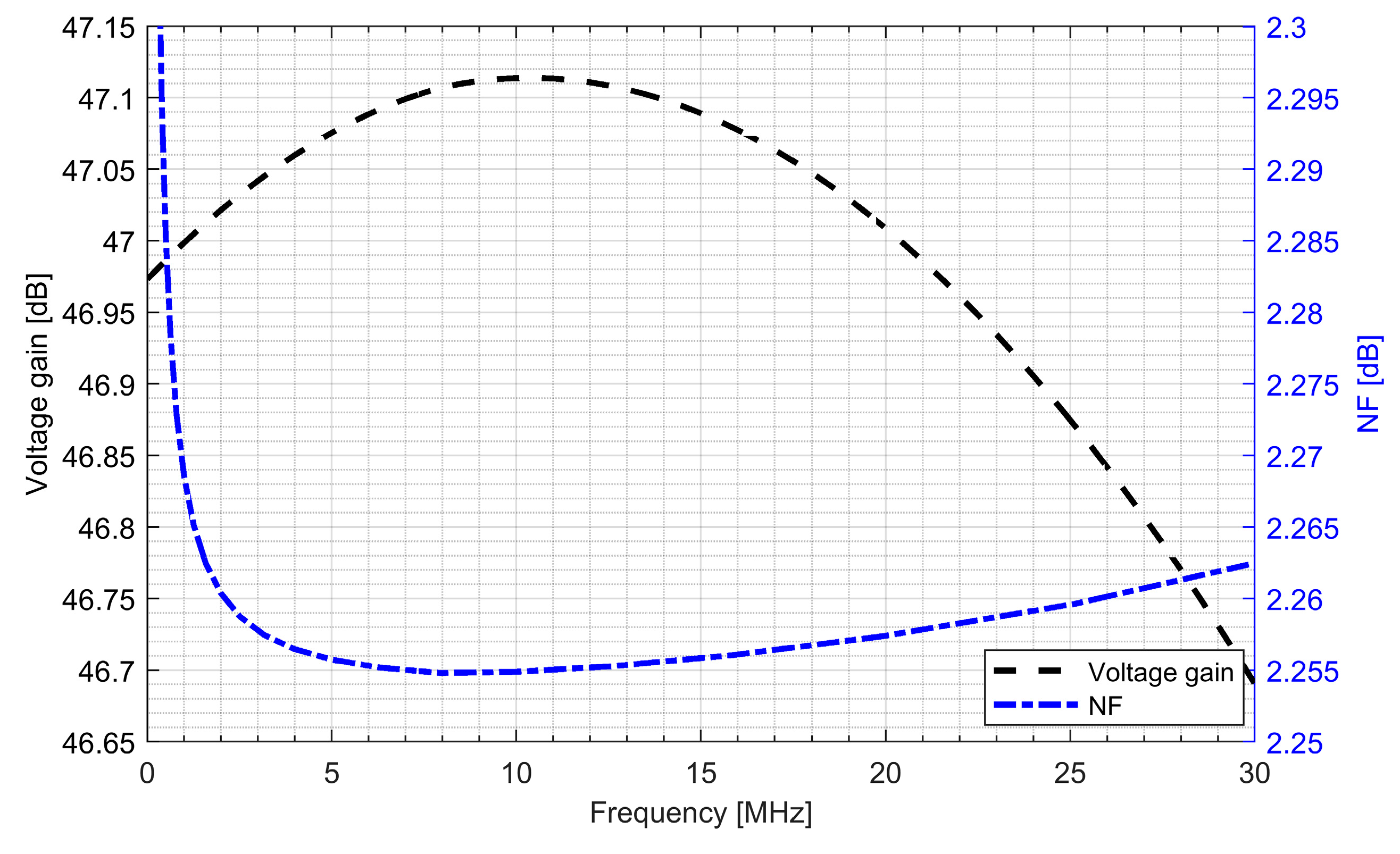
The whole radio-frequency front-end was verified. Figure 13 and Figure 14 show the conversion gain and noise figure results for the L1/E1 and the L5/E5 front-ends. It can be seen that for the L1/E1, the conversion gain was around 46.4 dB and the variation within the band was ±0.2 dB. The noise figure for the L1/E1 band was kept below 2.4 dB. For the L5/E5 band, the conversion gain was around 47 dB and the variation within the band was ±0.3 dB. The noise figure for the L5/E5 band was kept below 2.3 dB. The total power consumption of the L1/E1 and the L5/E5 front-ends were both around 5.1 mW (3.4 mA from 1.5 V supply voltage).
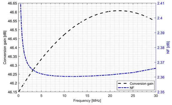
Figure 13.
Conversion gain and noise figure of the L1/E1 radio-frequency front-end.
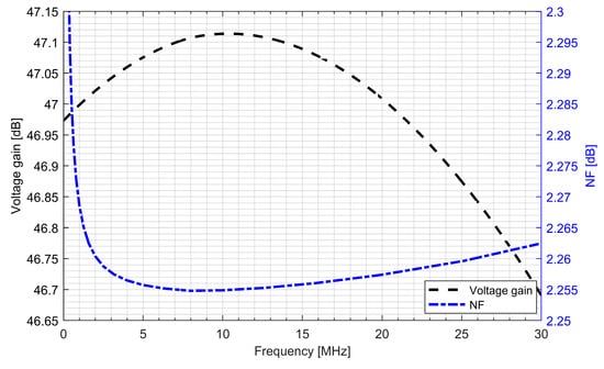
Figure 14.
Conversion gain and noise figure of the L5/E5 radio-frequency front-end.
3.4. Intermediate Frequency Block and ADC
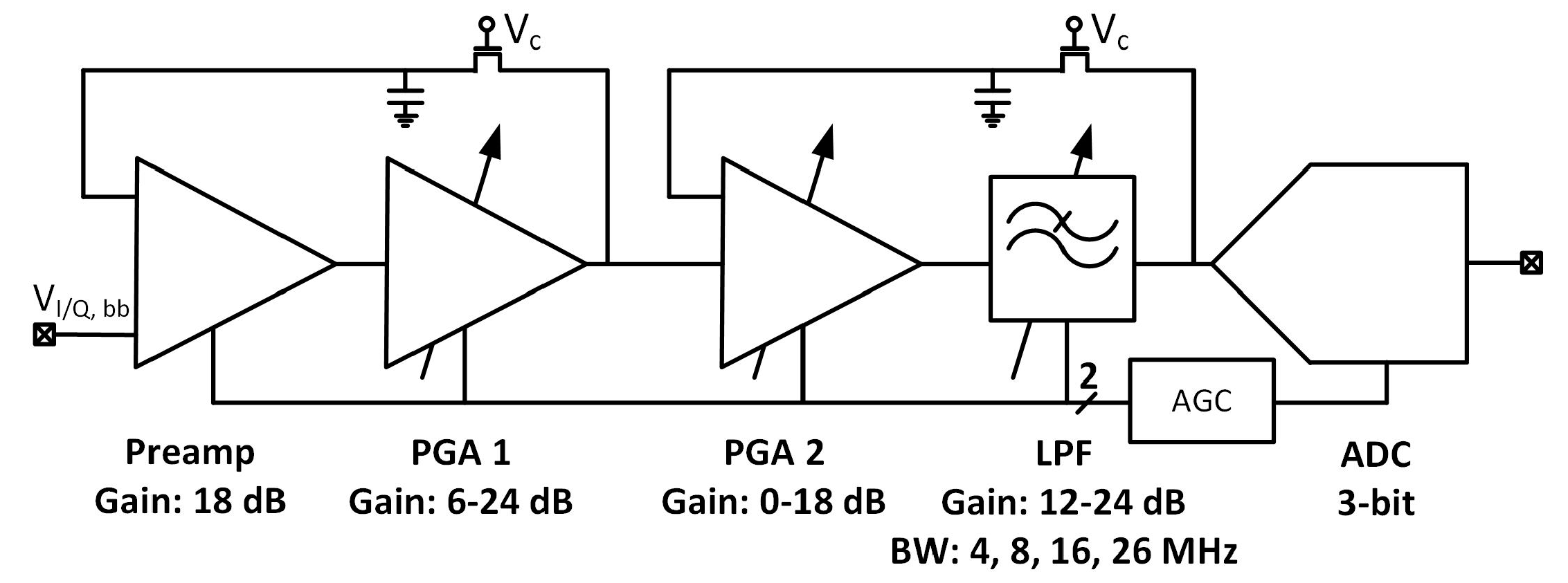
The intermediate frequency signal processing chain was composed of four gain stages and a 3-bit SAR (successive approximation) ADC. Figure 15 shows the block diagram of the implemented analog IF with ADC. For clarity, only in-phase path and single-ended versions of the I/Q chain are presented.

Figure 15.
Block diagram of dual-frequency analog IF and ADC.
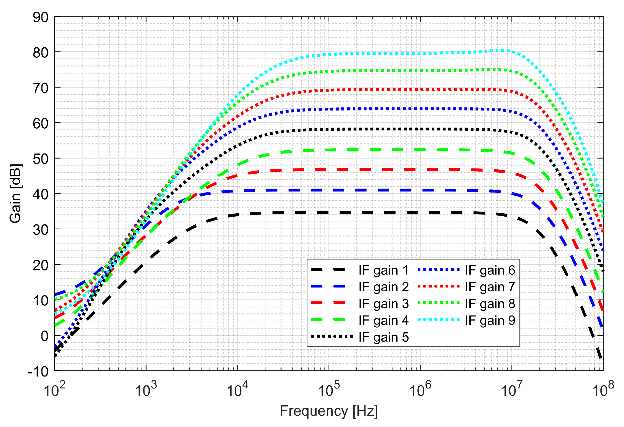
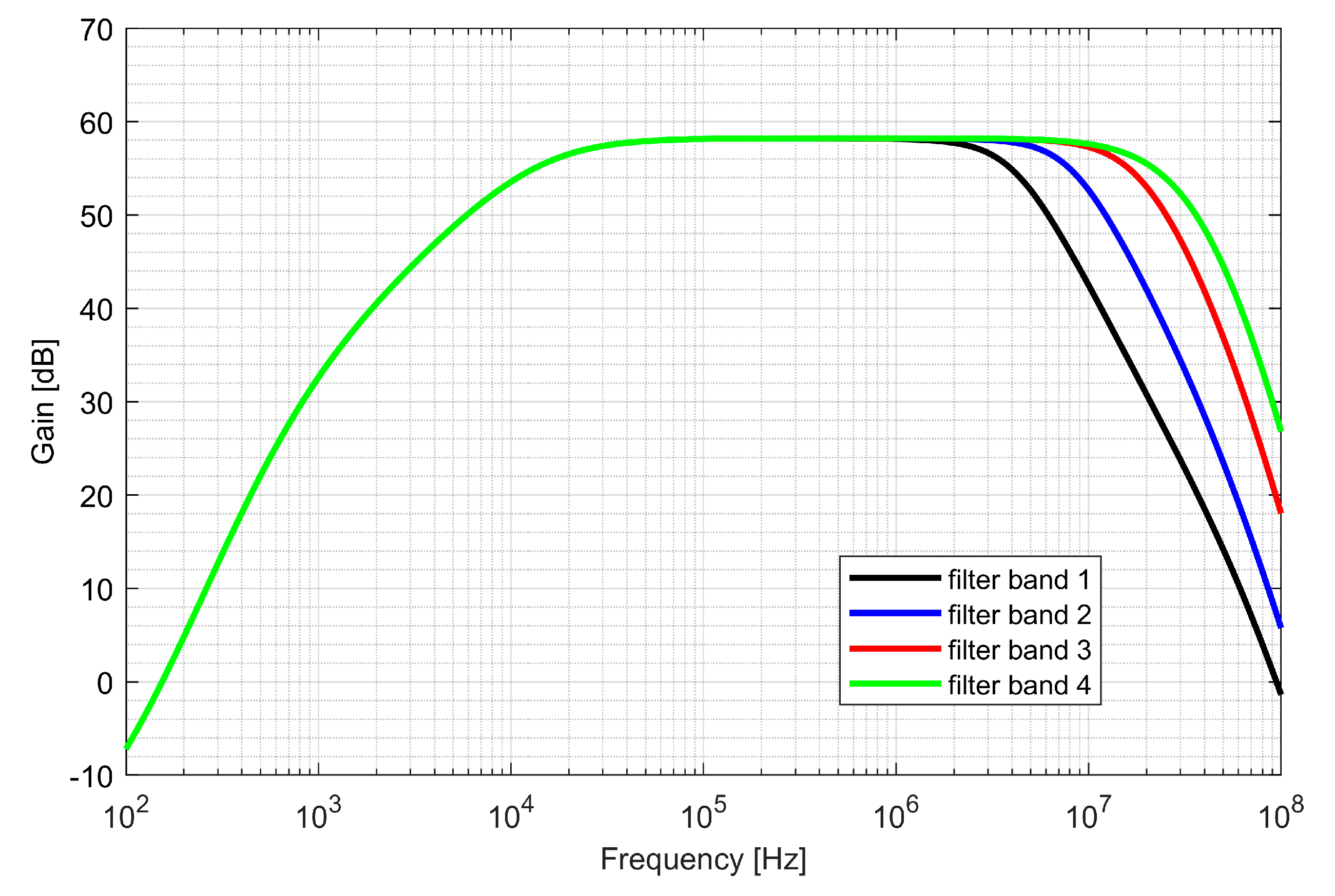
The first stage—preamplifier was optimized for low noise. The gain of the PGAs and low-pass filter (LPF) is programmable, allowing a 48 dB dynamic range to be obtained. The bandwidth of LPF is configurable to 4, 8, 16, 26 MHz and sets the overall cutoff frequency of the I/Q baseband. In order to avoid saturation of the blocks, two DC (direct current) offset cancellation (DCOC) loops were employed. The DC offset was filtered with a pseudo-resistor low-pass filter and subtracted in the preamplifier and the PGA2, which were designed as double differential amplifiers. The DCOC loops set the overall high-pass cutoff frequency to 50 kHz to avoid slow settling without compromising signal integrity. A digital automatic gain control (AGC) circuit was included to ensure a constant signal magnitude at the ADC input. The whole dual-frequency I/Q IF chain with ADC included draws 6.2 mA from a 1.5 V supply. The input referred RMS noise of IF integrated from 100 kHz to 32 MHz is 46 µV. Both supply and ground were separated between the analog and mixed-signal parts of the baseband to avoid interferences. Figure 16 and Figure 17 show the IF chain gain characteristics for gain and band sweep, respectively.
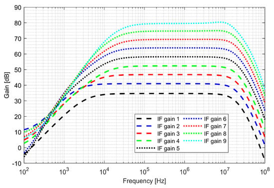
Figure 16.
Gain characteristics of the intermediate frequency (IF) chain for different gain settings.
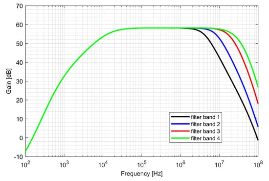
Figure 17.
Gain characteristics of the intermediate frequency chain for different band settings.
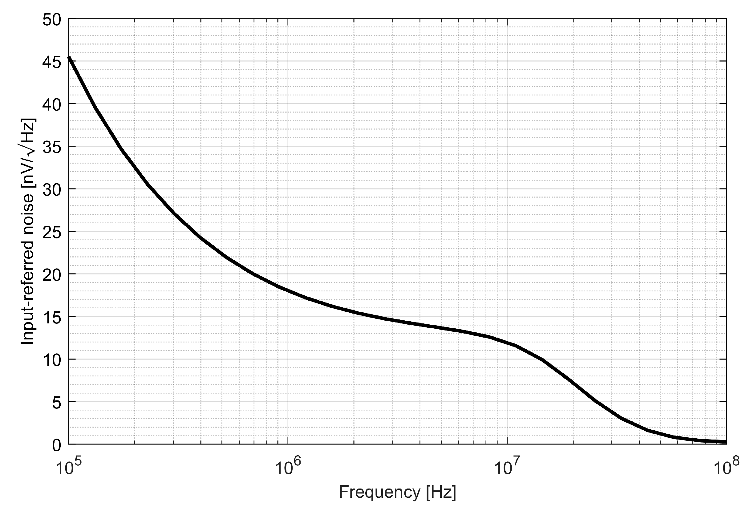
The input referred voltage noise is presented in Figure 18. It can be seen that the voltage noise density is kept below 20 nV/√Hz and above 1 MHz. To verify the impact of the IF chain noise on the overall system performance, the noise resulting from previous stages was calculated as
where k is the Boltzmann constant, T is the temperature in Kelvins, RANT is antenna impedance, FRF is RF the front-end noise figure in a linear scale and GRF is the total voltage gain of the RF front-end. Antenna resistance is equal to 50 Ω, temperature is equal to 300 K and L1/E1 RF front-end the noise is equal to 120 nV/√Hz. As this value is much higher than the noise of the IF chain, it can be concluded that the IF chain noise does not have an important impact on the overall system performance.
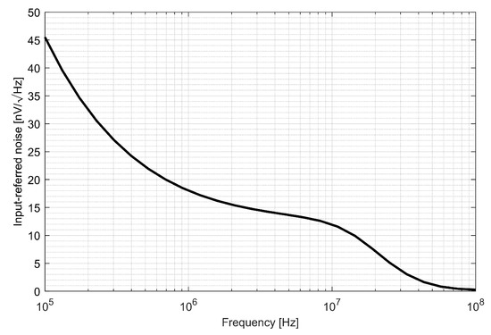
Figure 18.
Intermediate frequency noise characteristics.
3.5. Frequency Synthesizer and I/Q LO Signal Generation
The local oscillator (LO) block was used to generate quadrature signals for the mixer. In the GNSS receiver designed, it was important to achieve both low phase noise and a flexible frequency selection. The latter requirement requires the use of a fractional frequency synthesizer. To satisfy the specification and keep the power consumption low, an all-digital phase locked loop (ADPLL) was used. In ADPLL, the high frequency signal is generated in a digitally controlled oscillator (DCO) and the signal frequency is determined by a series of bits. To obtain high accuracy of the output signal frequency, it was necessary to implement a full custom designed MOM (Metal-Oxide-Metal) capacitor with a very small capacitance value.
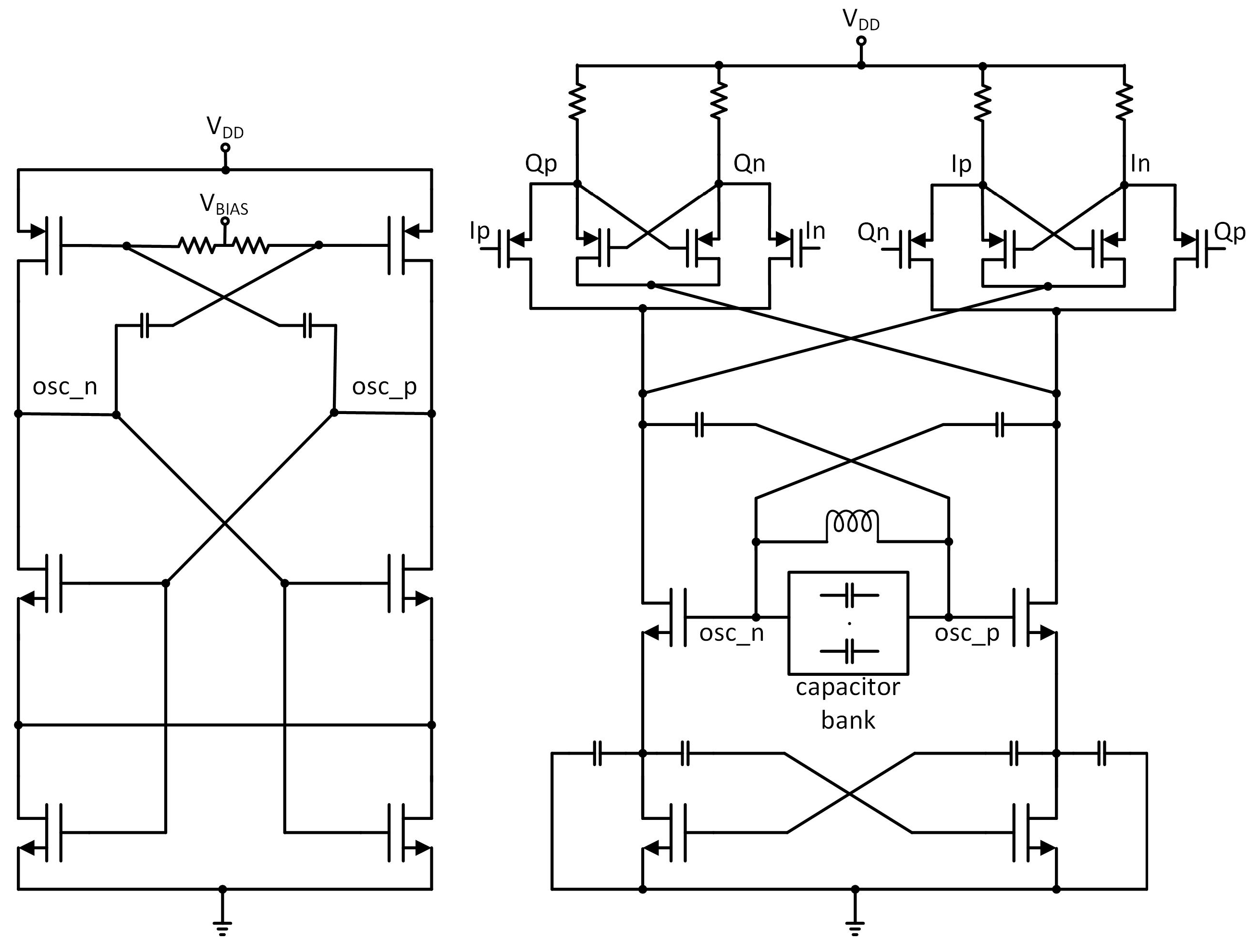
In ADPLL design there is a tradeoff between phase noise and power consumption. The DCO is the most critical block as it is usually responsible for around 70% of the dissipated power in the frequency synthesizer circuit. To generate quadrature signals, the DCO was designed to work on two times higher frequency and its output is connected to a quadrature divider. To minimize the dissipated power, a frequency divider was stacked on the Colpitts DCO [23]. The Colpitts oscillator architecture was chosen because it has less phase noise and can work with a lower supply voltage in comparison to cross-couple oscillators. On the other hand, a Colpitts generator requires a higher negative-gm to satisfy the startup conditions when compared with a cross-coupled generator. This leads to increased power consumption. For this reason, the typical Colpitts architecture was modified by adding a cross-coupled transistor pair to relax the startup conditions and reduce power consumption (see Figure 19).
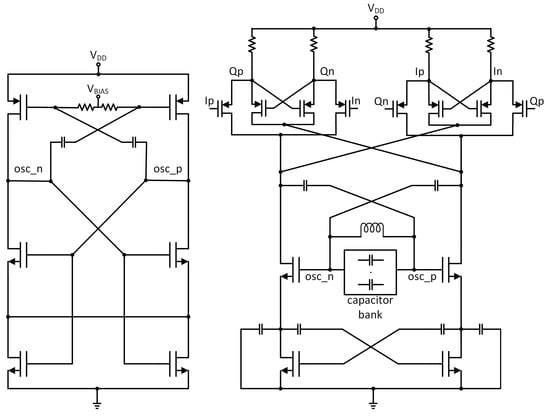
Figure 19.
Simplified schematic diagram of the designed digitally controlled oscillator (DCO).
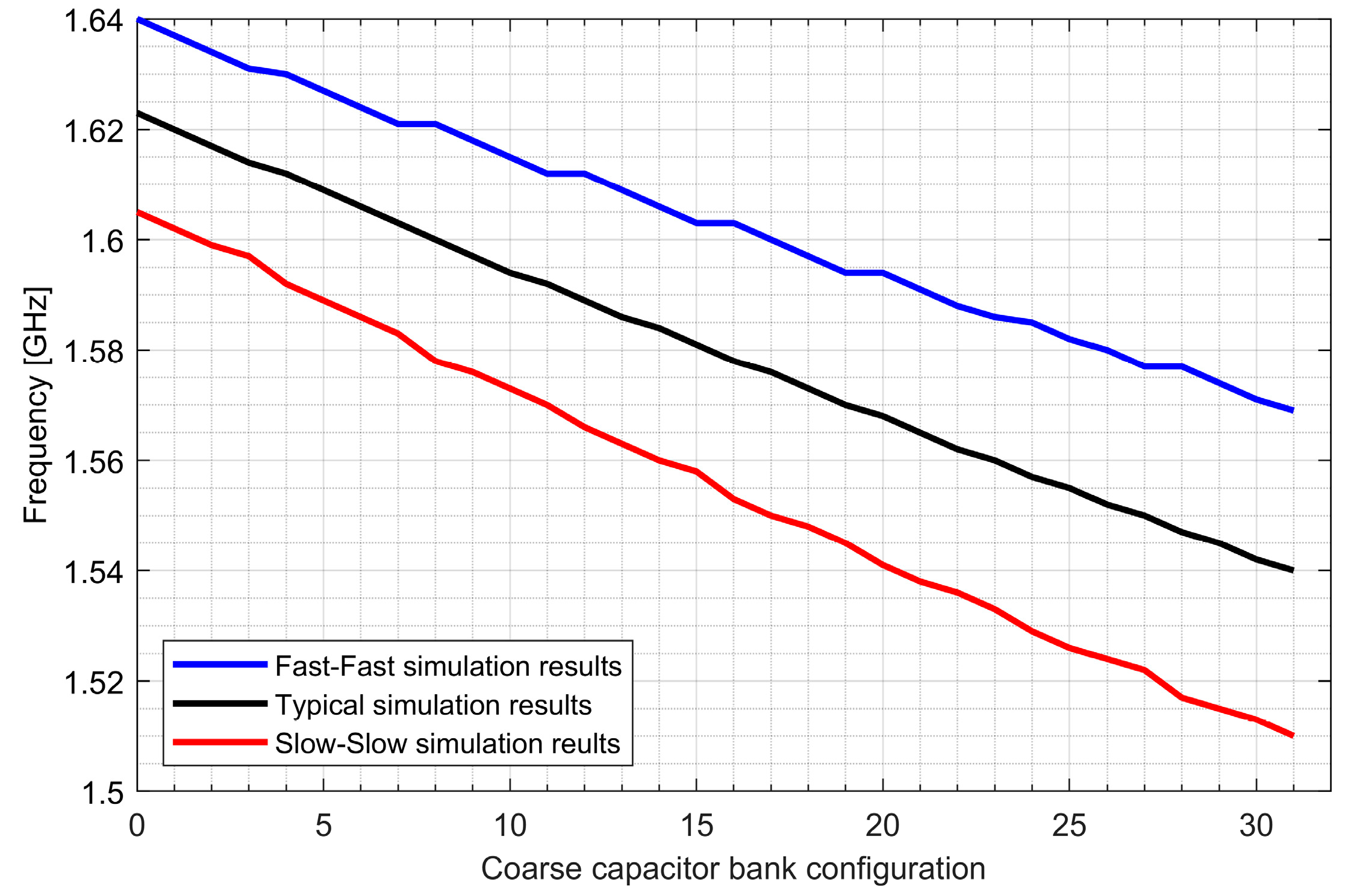
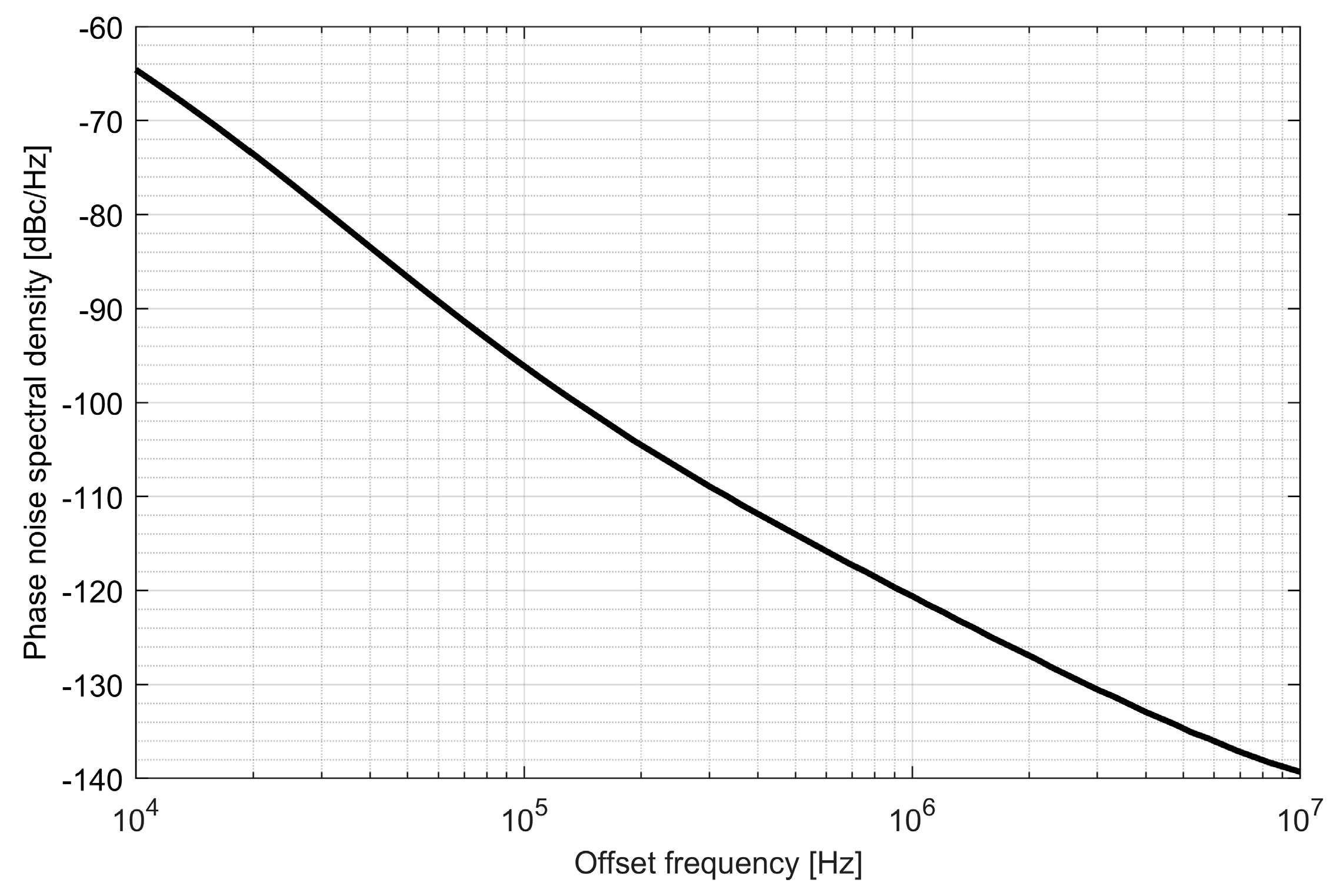
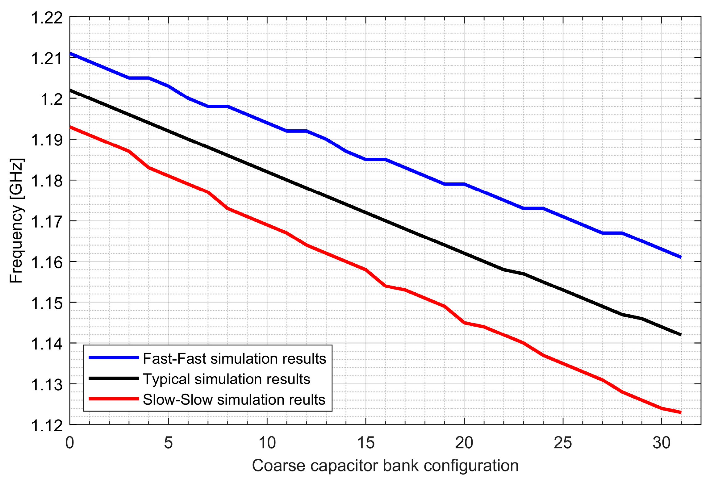
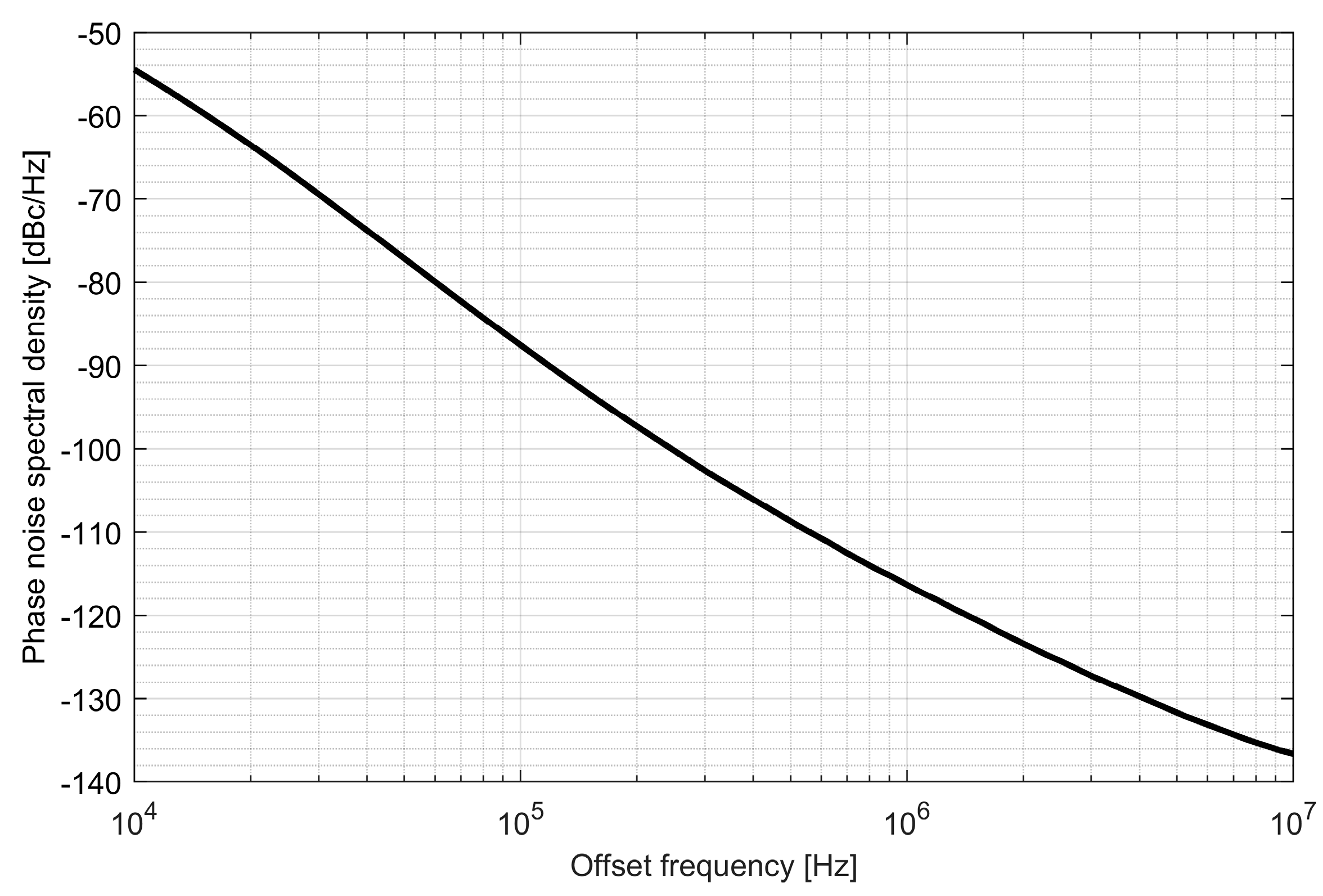
Two ADPLLs for the L1/E1 and L5/E5 bands were implemented in the GNSS SoC. The phase noise of each frequency synthesizer equals −121 dBc/Hz at 1 MHz from the carrier frequency, while 4.5 mA is consumed from a 1.5 V supply. The post-layout DCO simulation tuning characteristics and phase noise are presented in Figure 20, Figure 21, Figure 22 and Figure 23.
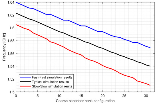
Figure 20.
Tuning characteristics of the L1/E1 digitally controlled oscillator.
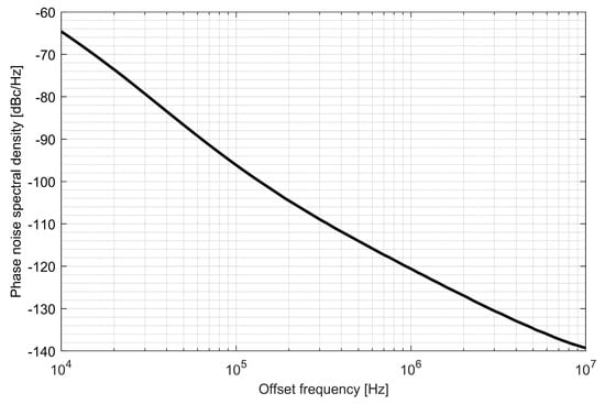
Figure 21.
Phase noise of the L1/E1 digitally controlled oscillator.

Figure 22.
Tuning characteristics of the L5/E5 digitally controlled oscillator.
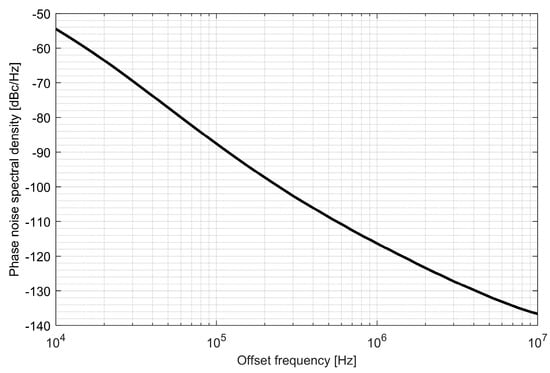
Figure 23.
Phase noise of the L5/E5 digitally controlled oscillator.
4. System-on-Chip Verification
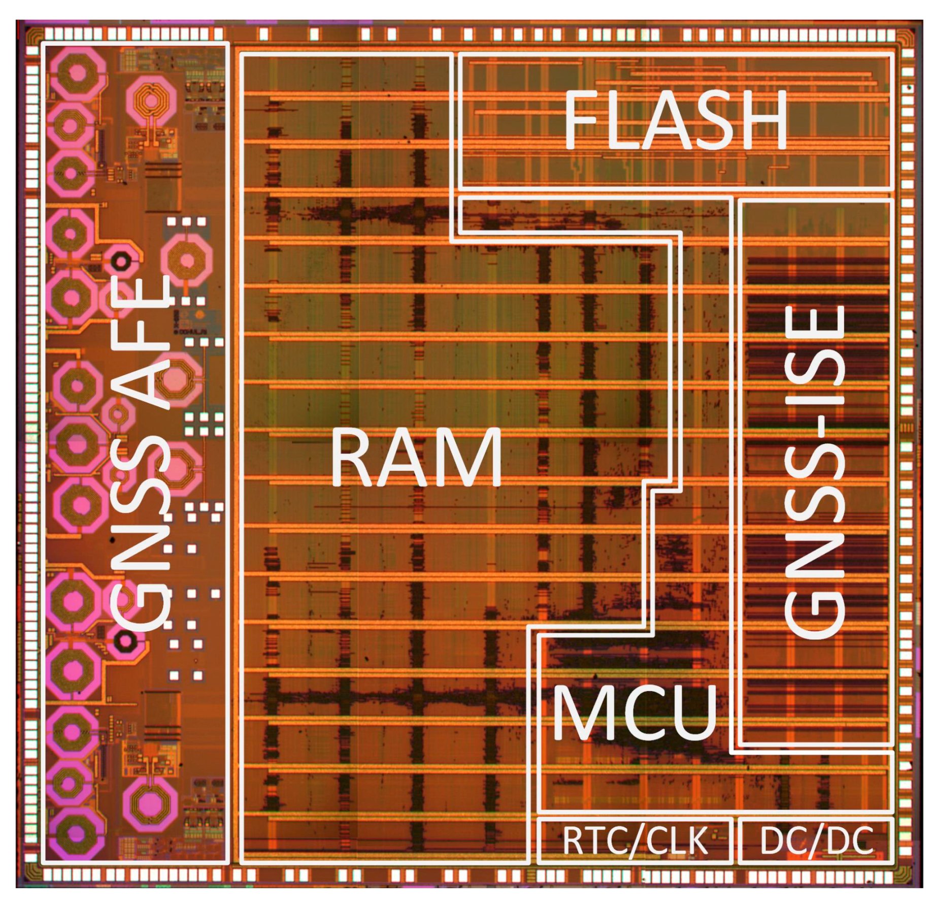
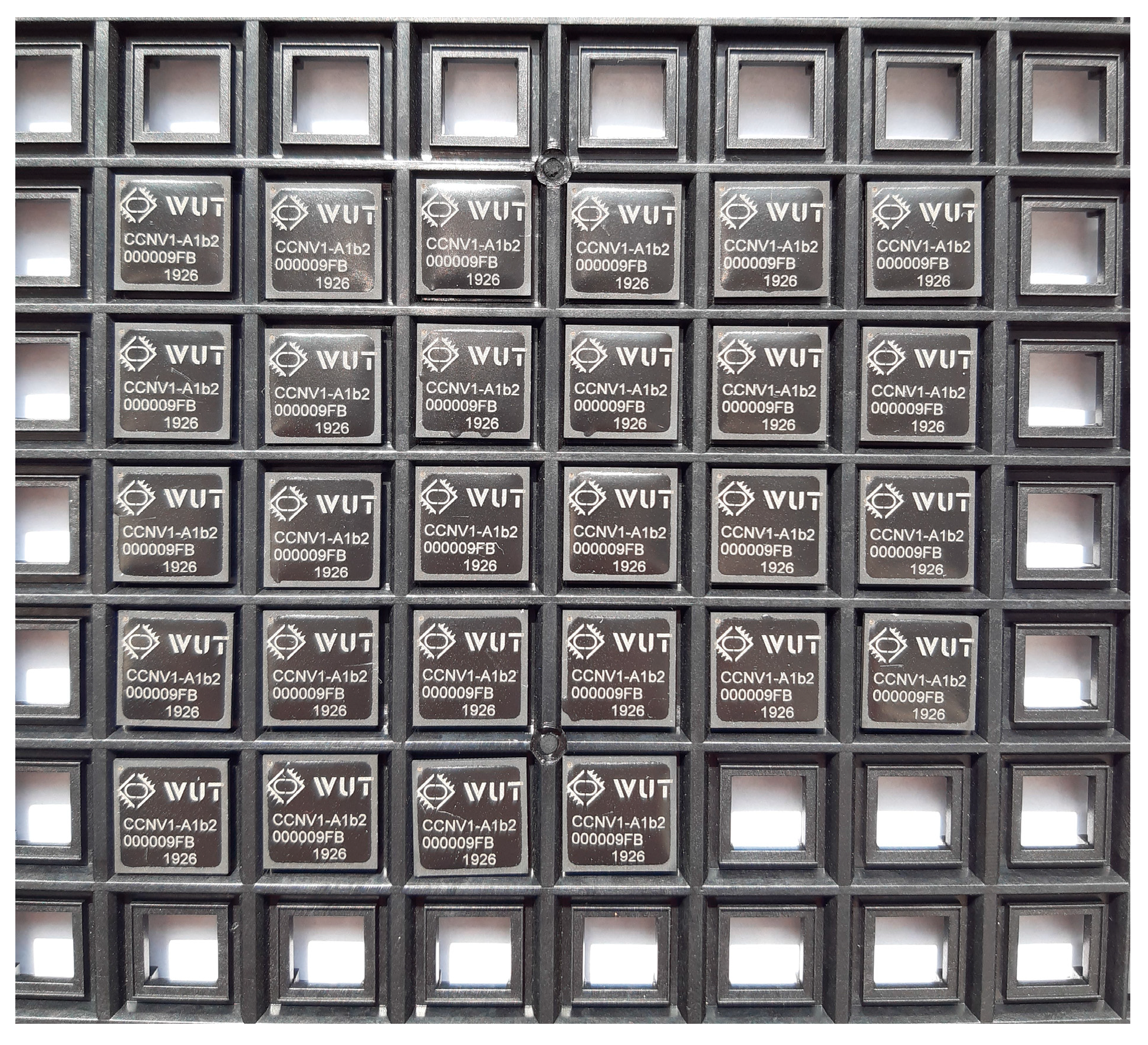
A complete dual-frequency single-chip GNSS receiver including radio was implemented in a 110 nm CMOS technology (see Figure 24 and Figure 25). A two-wideband of 52 MHz high gain RF AFE of 131 dB with NF 2.3 dB was integrated with a triple-core 32-bit RISC navigation and application processor with user accessible eFlash. The radio part includes the LNAs, active baluns, mixers, ADPLLs and IF with I/Q ADCs. The total chip area is 34 mm2. The chip used has been manufactured and is currently in the measurement phase (see Figure 26). The manufactured SoC has been successfully used to acquire the GNSS signals using an in-house developed antenna (see Figure 27). The acquisition time used was 1 ms and the SNR (signal-to-noise ratio) obtained was 16.4 dB. The CCNV1_A1 was also used to develop positioning software.
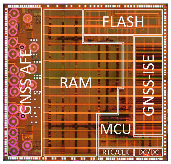
Figure 24.
CCNV1-A1 integrated circuit die microphotography.
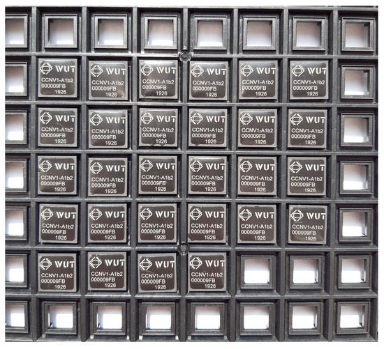
Figure 25.
CCNV1-A1 packaged dies.
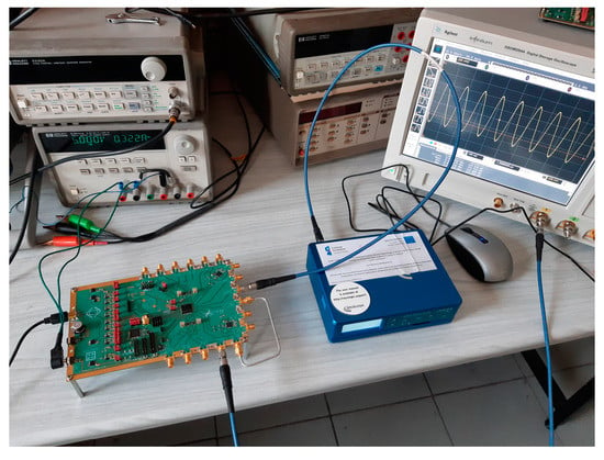
Figure 26.
CCNV1-A1 measurement environment with the evaluation board. The photo presents the CCNV1-A1 measurement board connected to the LabSat 3 GNSS Simulator and DSO90254A Digital Storage Oscilloscope.
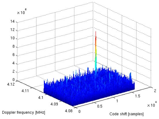
Figure 27.
GPS L1 acquisition results obtained with a CCNV1-A1 and in-house developed antenna with a 1 ms acquisition time.
All the presented results are post-layout simulation-based. Table 1 summarizes the performance of the presented dual-frequency receiver and a comparison with the state-of-the-art parameters. The comparison indicates that this receiver supports most of the GNSS systems, simultaneously working with only two RF channels. Additionally, it is important to mention that ultra-low leakage technology with metal stack on aluminum was chosen. Its parameters, such as connection resistance, inductance quality factor, and a high Vt of transistors, are unfavorable for analog and RF design in particular, which should be taken into account during the comparison.

Table 1.
Comparison with previously published multiband GNSS receivers.
5. Conclusions
The main concept of this work was to integrate a dual-frequency, multi-system GNSS receiver into one integrated circuit. In the introduction, it is explained why this integration provides improvements in terms of both precision and reliability. The SoC was designed in a 110 nm ultra-low leakage device with an aluminum metal stack. This is cost effective but poses technical challenges. It was shown that even using such technology, it is possible to achieve state-of-the-art parameters. The receiver covers both L1/E1 and L5/E5 bands for all available GNSS signals with the channel bandwidth configurable from 8 MHz to 52 MHz. Due to the design architecture used, the noise figure can be maintained within the lowest range compared to the existing solutions which have the highest bandwidth. The implemented dual-frequency GNSS AFE is highly configurable in terms of center frequency, channel bandwidth and ADC sampling rate, to customize the CCNV1-A1 positioning accuracy performance vs. power consumption for different types of applications. The accompanying GNSS-ISE baseband engine comprises highly configurable tracking-loops as well as versatile PRN (pseudo random noise) code generators (primary and secondary) to cover all mentioned GNSS systems. Currently, navigation software covering acquisition, tracking and positioning is being developed. The final SoC version including advanced power management has been designed.
Author Contributions
The work presented in this paper was a collaboration of all Authors. Methodology, investigation and validation of RF and analog design, visualization, writing—original draft preparation, T.B. (RF system architecture), K.S. (specification, LO design—ADPLL control), P.N. (power management, current and voltage references, POR design), A.B. (power management, DCDC converter), I.B. (LO design—DCO), D.P. (RF design—LNA, balun and mixer), S.R. (clock generation design), Ł.W. (IF design); methodology, investigation and validation of digital design, visualization, writing—original draft preparation; K.M. (microprocessor and GNSS baseband), A.Ł. (SoC floorplan, backend and sign-off), M.P. (microcontroller peripherals and flash controller); supervision, writing—review and editing, project administration, funding acquisition, W.A.P. All authors have read and agreed to the published version of the manuscript.
Funding
This work was co-funded by the European Union from the European Regional Development Fund under the Smart Growth Operational Programme 2014–2020, Sub-Measure 4.1.4 Application Projects under grant no. POIR.04.01.04-00-0101/16.
Conflicts of Interest
The authors declare no conflict of interest.
References
- Fernandez-Prades, C.; Lo Presti, L.; Falletti, E. Satellite Radiolocalization From GPS to GNSS and Beyond: Novel Technologies and Applications for Civil Mass Market. Proc. IEEE 2011, 99, 1882–1904. [Google Scholar] [CrossRef]
- GNSS Market Report, Issue 5, Publications Office of the European Union, Copyright© European GNSS Agency. 2017. Available online: https://www.gsa.europa.eu/system/files/reports/gnss_mr_2017.pdf (accessed on 16 November 2019).
- Kadoyama, T.; Suzuki, N.; Sasho, N.; Iizuka, I.; Nagase, I.; Usukubo, H.; Katakura, M. A complete single-chip GPS receiver with 1.6-V 24-mW radio in 0.18-µm CMOS. IEEE J. Solid-State Circuits 2004, 39, 562–568. [Google Scholar] [CrossRef]
- Sahu, D.; Das, Q.; Darwhekar, Y.; Ganesan, S.; Rajendran, G.; Kumar, R.; Chandrashekar, B.G.; Gosh, A.; Gaurav, A.; Krishnaswamy, T.; et al. A 90 nm CMOS single-chip GPS receiver with 5 dBm out-of-band IIP3 and 2.0 dB NF. In Proceedings of the IEEE International Digest of Technical Papers. Solid-State Circuits Conference, San Francisco, CA, USA, 10 February 2005; pp. 308–309. [Google Scholar] [CrossRef]
- Gramegna, G.; Mattos, P.G.; Losi, M.; Das, S.; Franciotta, M.; Bellantone, N.G.; Vaiana, M.; Mandara, V.; Paparo, M. A 56-mVienna, AustriaW 23-mm2 single-chip 180-nm CMOS GPS receiver with 27.2-mW 4.1-mm2 radio. IEEE J. Solid State Circuits 2006, 41, 540–551. [Google Scholar] [CrossRef]
- Wei, J.-M.; Chen, C.-N.; Chen, K.-T.; Kuo, C.-F.; Ong, B.-H.; Lu, C.-H.; Liu, C.-C.; Chiou, H.-C.; Yeh, H.-C.; Shieh, J.-H.; et al. A 110 nm RFCMOS GPS SOC with 34 mW -165dBm tracking sensitivity. In Proceedings of the IEEE International Digest of Technical Papers. Solid-State Circuits Conference, San Francisco, CA, USA, 8–12 February 2009; pp. 254–255. [Google Scholar] [CrossRef]
- Moon, H.; Lee, S.; Heo, S.-C.; Yu, H.; Yu, J.; Chang, J.-S.; Choi, S.-I.; Park, B.-H. A 23 mW fully integrated GPS receiver with robust interferer rejection in 65 nm CMOS. In Proceedings of the IEEE International Digest of Technical Papers. Solid-State Circuits Conference, San Francisco, CA, USA, 7–11 February 2010; pp. 68–69. [Google Scholar] [CrossRef]
- Wu, C.-H.; Tsai, W.-C.; Tan, C.-G.; Chen, C.-N.; Li, K.-I.; Hsu, J.-L.; Lo, C.-L.; Chen, H.-H.; Su, S.-Y.; Chen, K.-T.; et al. A GPS/Galileo SoC with adaptive in-band blocker cancellation in 65 nm CMOS. In Proceedings of the 2011 IEEE International Solid-State Circuits Conference, San Francisco, CA, USA, 20–24 February 2011; pp. 462–464. [Google Scholar]
- Tan, C.G.; Song, F.; Choke, T.Y.; Kong, M.; Song, D.-C.; Yong, C.-H.; Shu, W.; You, Z.H.; Lin, Y.-H.; Shanaa, O. A universal GNSS (GPS/Galileo/Glonass/Beidou) SoC with a 0.25 mm2 radio in 40 nm CMOS. In Proceedings of the IEEE International Digest of Technical Papers. Solid-State Circuits Conference, San Francisco, CA, USA, 17–21 February 2013; pp. 334–335. [Google Scholar] [CrossRef]
- Skournetou, D.; Lohan, E.-S. Ionospheric delay corrections in multi-frequency receivers: Are three frequencies better than two? In Proceedings of the 2011 International Conference on Localization and GNSS (ICL-GNSS), Tampere, Finland, 29–30 June 2011; pp. 181–186. [Google Scholar] [CrossRef]
- Kaplan, E.D.; Hegarty, C. Understanding GPS/GNSS: Principles and Applications, 3rd ed.; Artech House: Boston, MA, USA, 2017. [Google Scholar]
- Jiang, Z.; Groves, P.D.; Ochieng, W.Y.; Feng, S.; Milner, C.D.; Mattos, P.G. Multi-Constellation GNSS Multipath Mitigation Using Consistency Checking. In Proceedings of the 24th International Technical Meeting of The Satellite Division of the Institute of Navigation (ION GNSS 2011), Portland, OR, USA, 20–23 September 2011; pp. 3889–3902. [Google Scholar]
- Detratti, M.; Lopez, E.; Perez, E.; Palacio, R.; Lobeira, M. Dual-band RF receiver chip-set for Galileo/GPS applications. In Proceedings of the IEEE/ION Position, Location and Navigation Symposium, Monterey, CA, USA, 5–8 May 2008; pp. 851–859. [Google Scholar] [CrossRef]
- Moon, Y.; Cha, S.; Kim, G.; Park, K.; Ko, S.; Park, H.; Park, J.; Lee, J. A 26mW dual-mode RF receiver for GPS/Galileo with L1/L1F and L5/E5a bands. In Proceedings of the IEEE International SoC Design Conference, Busan, Korea, 24–25 November 2008; p. I-421. [Google Scholar] [CrossRef]
- Qi, N.; Xu, Z.; Chi, B.; Xu, Z.; Yu, X.; Zhang, X.; Xu, N.; Chiang, P.; Rhee, W.; Wang, Y. A Dual-Channel Compass/GPS/GLONASS/Galileo Reconfigurable GNSS Receiver in 65 nm CMOS With On-Chip I/Q Calibration. IEEE Trans. Circuits Syst. I 2012, 59, 1720–1732. [Google Scholar] [CrossRef]
- Chen, D.; Pan, W.; Jiang, P.; Jin, J.; Mo, T.; Zhou, J. Reconfigurable Dual-Channel Multiband RF Receiver for GPS/Galileo/BD-2 Systems. IEEE Trans. Microw. Theory Tech. 2012, 60, 3491–3501. [Google Scholar] [CrossRef]
- Garzia, F.; Kohler, S.; Urquijo, S.; Neumaier, P.; Driesen, J.; Haas, S.; Leineweber, T.; Zhang, T.; Krause, S.; Henkel, F.; et al. NAPA: A fully integrated multi-constellation two-frequency single-chip GNSS receiver. In Proceedings of the 2014 IEEE/ION Position, Location and Navigation Symposium (PLANS 2014), Monterey, CA, USA, 5–8 May 2014; pp. 1075–1083. [Google Scholar] [CrossRef]
- Jo, I.; Bae, J.; Matsuoka, T.; Ebinuma, T. RF front-end architecture for a triple-band CMOS GPS receiver. Microelectron. J. 2015, 46, 27–35. [Google Scholar] [CrossRef]
- Li, S.; Li, J.; Gu, X.; Wang, H.; Li, C.; Wu, J.; Tang, M. Reconfigurable All-Band RF CMOS Transceiver for GPS/GLONASS/Galileo/Beidou With Digitally Assisted Calibration. IEEE Trans. Very Large Scale Integr. Syst. 2015, 23, 1814–1827. [Google Scholar] [CrossRef]
- NaviSoC Project. Available online: http://navisoc.com/ (accessed on 22 December 2019).
- Marcinek, K.; Pleskacz, W.A. GNSS-ISE: Instruction Set Extension for GNSS Baseband Processing. Sensors 2020, 20, 465. [Google Scholar] [CrossRef] [PubMed]
- Navipedia, European Space Agency Science GNSS Science Support Centre. Available online: https://gssc.esa.int/navipedia (accessed on 16 November 2019).
- Ji, X.; Wu, J.; Shi, L. Current reused Colpitts VCO and frequency divider for quadrature generation. In Proceedings of the International Conference on Electric Information and Control Engineering, Wuhan, China, 15–17 April 2011; pp. 256–259. [Google Scholar] [CrossRef]
© 2020 by the authors. Licensee MDPI, Basel, Switzerland. This article is an open access article distributed under the terms and conditions of the Creative Commons Attribution (CC BY) license (http://creativecommons.org/licenses/by/4.0/).

