
Plasmonic Field-Effect Transistors (TeraFETs) for 6G Communications


Abstract
:
1. Introduction
2. Plasmonic TeraFETs
3. Plasmonic Crystals
4. TeraFET Sources
5. Other TeraFET Applications
6. Conclusions
Author Contributions
Funding
Institutional Review Board Statement
Informed Consent Statement
Data Availability Statement
Conflicts of Interest
References
- Labovitz, C. Early Effects of COVID-19 Lockdowns on Service Provider Networks: The Networks Soldier on! Available online: https://www.nokia.com/blog/early-effects-covid-19-lockdowns-service-provider-networks-networks-soldier/ (accessed on 20 March 2020).
- Dhillon, S.S.; Vitiello, M.S.; Linfield, E.H.; Davies, A.; Hoffmann, M.; Booske, J.; Paoloni, C.; Gensch, M.; Weightman, P.; Williams, G.P.; et al. The 2017 terahertz science and technology roadmap. J. Phys. D Appl. Phys. 2017, 50, 043001. [Google Scholar] [CrossRef]
- Chowdhury, M.Z.; Shahjalal, M.; Ahmed, S.; Jang, Y.M. 6G Wireless Communication Systems: Applications, Requirements, Technologies, Challenges, and Research Directions. IEEE Open J. Commun. Soc. 2020, 1, 957–975. [Google Scholar] [CrossRef]
- Zhou, Y.; Liu, L.; Wang, L.; Hui, N.; Cui, X.; Wu, J.; Peng, Y.; Qi, Y.; Xing, C. Service-aware 6G: An intelligent and open network based on the convergence of communication, computing and caching. Digit. Commun. Netw. 2020, 6, 253–260. [Google Scholar] [CrossRef]
- O’Dea, S. Connection Density of 4G, 5G and 6G Technology, 19 November 2020. Available online: https://www.statista.com/statistics/1183690/mobile-broadband-connection-density/ (accessed on 22 November 2021).
- Pala, N.; Shur, M. THz Photonic and Plasmonic Devices for Sensing, Imaging and Communication Applications, SPIE Defense + Commercial Sensing. In Proceedings of the Micro- and Nanotechnology Sensors, Systems and Applications XI, Baltimore, MD, USA, 13 May 2019; Volume 10982, p. 109822Y. [Google Scholar] [CrossRef]
- Lee, S.; Hara, S.; Yoshida, T.; Amakawa, S.; Dong, R.; Kasamatsu, A.; Sato, J.; Fujishima, M. An 80-Gb/s 300-GHz-Band Single-Chip CMOS Transceiver. IEEE J. Solid-State Circuits 2019, 54, 3577–3588. [Google Scholar] [CrossRef]
- Fujishima, M. Overview of sub-terahertz communication and 300GHz CMOS transceivers. IEICE Electron. Express 2021, 18, 20212002. [Google Scholar] [CrossRef]
- Kürner, T.; Kallfass, I.; Ajito, K.; Kasamatsu, A.; Britz, D.; Priebe, S. “What’s Next? Wireless Communication beyond 60 GHz,” Tutorial of IEEE 802.15 IG THz, IEEE 802 Plenary. 2012. Available online: https://mentor.ieee.org/802.15/dcn/12/15-12-0320-02-0thz-what-s-next-wireless-communication-beyond-60-ghz-tu-torial-ig-thz.pdf (accessed on 22 November 2021).
- Bhat, J.R.; AlQahtani, S.A. 6G Ecosystem: Current Status and Future Perspective. IEEE Access 2021, 26, 43134–43136. [Google Scholar] [CrossRef]
- NTT DOCOMO, Inc. White Paper 5G Evolution and 6G. 2020. Available online: www.nttdocomo.co.jp/english/binary/pdf/corporate/technology/ (accessed on 22 November 2021).
- Shur, M. Pandemic Equation for Describing and Predicting COVID-19 Evolution. J. Health Inform. Res. 2021, 5, 168–180. [Google Scholar] [CrossRef]
- IEEE. IEEE Standard for High Data Rate Wireless Multi-Media Networks—Amendment 2:100 Gb/s Wireless Switched Point-to-Point Physical Layer; IEEE Standard 802.15.3d-2017; IEEE: Piscataway, NJ, USA, 2017. [Google Scholar]
- Shur, M.; Gaska, R. Device and Method for Managing Radiation. U.S. Patent 7638817, 29 December 2009. [Google Scholar]
- Shur, M.; Ryzhii, V.; Gaska, R. Method of Radiation Generation and Manipulation. U.S. Patent 7,619,263, 17 November 2009. [Google Scholar]
- Petrov, A.S.; Svintsov, D.; Ryzhii, V.; Shur, M.S. Amplified-reflection plasmon instabilities in grating-gate plasmonic crystals. Phys. Rev. B 2017, 95, 045405. [Google Scholar] [CrossRef] [Green Version]
- Karabiyik, M.; Ahmadivand, A.; Sinha, R.; Al-Amin, C.; Vabbina, P.K.; Kaya, S.; Rupper, G.; Rudin, S.; Shur, M.; Pala, N. Plasmonic properties of asymmetric dual grating gate plasmonic crystals. Phys. Status Solidi B 2016, 253, 671–675. [Google Scholar] [CrossRef]
- Teperik, T.V.; De Abajo, F.J.G.; Popov, V.; Shur, M. Strong terahertz absorption bands in a scaled plasmonic crystal. Appl. Phys. Lett. 2007, 90, 251910. [Google Scholar] [CrossRef] [Green Version]
- Kachorovskii, V.; Shur, M. Current-induced terahertz oscillations in plasmonic crystal. Appl. Phys. Lett. 2012, 100, 232108. [Google Scholar] [CrossRef]
- Aizin, R.; Mikalopas, J.; Shur, M. Current driven “plasmonic” instability in gated periodic ballistic nanostructures. Phys. Rev. B 2016, 93, 195315. [Google Scholar] [CrossRef] [Green Version]
- Dmitriev, A.; Kachorovskii, V.; Shur, M. Granular semiconductor/pyroelectric media as a tunable plasmonic crystal. Solid-State Electron. 2007, 51, 812–815. [Google Scholar] [CrossRef]
- Zhang, X.; Xu, Q.; Xia, L.; Li, Y.; Gu, J.; Tian, Z.; Ouyang, C.; Han, J.; Zhang, W. Terahertz surface plasmonic waves: A review. Adv. Photonics 2020, 2, 014001. [Google Scholar] [CrossRef]
- Karabiyik, M. Terahertz Plasmonic Devices. ProQuest ETD Collection for FIU. AAI10744516. 2017. Available online: https://digitalcommons.fiu.edu/dissertations/AAI10744516 (accessed on 22 November 2021).
- Aizin, G.; Mikalopas, J.; Shur, M.S. Giant Inverse Faraday Effect in Plasmonic Crystal Ring. arXiv 2019, arXiv:2109.14051. Available online: http://arxiv.org/abs/2109.14051 (accessed on 20 October 2021).
- Yeung, K.Y.M.; Chee, J.; Yoon, H.; Song, Y.; Kong, J.; Ham, D. Far-Infrared Graphene Plasmonic Crystals for Plasmonic Band Engineering. Nano Lett. 2014, 14, 2479–2484. [Google Scholar] [CrossRef] [Green Version]
- Daniel, M. Mittleman, Frontiers in Terahertz Sources and Plasmonics Nature Photonics, Volume 7, September 2013. Available online: www.nature.com/naturephotonics (accessed on 22 November 2021).
- Sugaya, T.; Kawano, Y. Frequency-Tunable Terahertz Plasmonic Structure Based on the Solid Immersed Method for Sensing. Sensors 2021, 21, 1419. [Google Scholar] [CrossRef]
- Zakharko, Y.; Graf, A.; Zaumseil, J. Plasmonic Crystals for Strong Light–Matter Coupling in Carbon Nanotubes. Nano Lett. 2016, 16, 6504–6510. [Google Scholar] [CrossRef] [PubMed] [Green Version]
- Dyer, G.C.; Aizin, G.R.; Preu, S.; Vinh, N.Q.; Allen, S.J.; Reno, J.L.; Shaner, E.A. Inducing an Incipient Terahertz Finite Plasmonic Crystal in Coupled Two Dimensional Plasmonic Cavities. Phys. Rev. Lett. 2012, 109, 126803. [Google Scholar] [CrossRef]
- Dyer, G.C.; Aizin, G.R.; Allen, S.J.; Grine, A.D.; Bethke, D.; Reno, J.L.; Shaner, E.A. Induced transparency by coupling of Tamm and defect states in tunable terahertz plasmonic crystals. Nat. Photonics 2013, 7, 925–930. [Google Scholar] [CrossRef] [Green Version]
- Aizin, G.R.; Dyer, G.C. Transmission line theory of collective plasma excitations in periodic two-dimensional electron systems: Finite plasmonic crystals and Tamm states. Phys. Rev. B 2012, 86, 235316. [Google Scholar] [CrossRef] [Green Version]
- Deng, X.; Li, L.; Enomoto, M.; Kawano, Y. Continuously Frequency-Tuneable Plasmonic Structures for Terahertz Bio-sensing and Spectroscopy. Sci. Rep. 2019, 9, 3498. [Google Scholar] [CrossRef] [PubMed] [Green Version]
- Schaafsma, M.C.; Rivas, J.G. Semiconductor plasmonic crystals: Active control of THz extinction. In Proceedings of the 2013 38th International Conference on Infrared, Millimeter, and Terahertz Waves (IRMMW-THz), Mainz, Germany, 1 September 2013; pp. 1–2. [Google Scholar] [CrossRef] [Green Version]
- Liu, X.; Ytterdal, T.; Shur, M. Line of sight THz detector using Si TeraFETs. In Proceedings of the 46th IRMMW-THz 2021 Conference, Chengdu, China, 29 August–3 September 2021. [Google Scholar]
- Liu, X.; Ytterdal, T.; Shur, M. Travelling Wave THz Spectrometer using Si TeraFETs. In Proceedings of the 46th IRMMW-THz 2021 Conference, Chengdu, China, 29 August–3 September 2021. [Google Scholar]
- Rumyantsev, S.; Liu, X.; Kachorovskii, V.; Shur, M. Homodyne phase sensitive terahertz spectrometer. Appl. Phys. Lett. 2017, 111, 121105. [Google Scholar] [CrossRef]
- Veksler, D.; Muravjov, A.; Stillman, W.; Pala, N.; Shur, M. Detection and Homodyne Mixing of Terahertz Gas Laser Radiation by Submicron GaAs/AlGaAs FETs. In Proceedings of the 2017 IEEE Sensors Conference, Atlanta, GA, USA, 28–31 October 2007; pp. 443–445. [Google Scholar]
- Gorbenko, I.; Kachorovski, V.Y.; Shur, M.S. Plasmonic polarization-sensitive detector of terahertz radiation. J. Phys. Conf. Ser. 2019, 1236, 012029. [Google Scholar] [CrossRef]
- Ikamas, K.; But, D.B.; Lisauskas, A. Homodyne Spectroscopy with Broadband Terahertz Power Detector Based on 90-nm Silicon CMOS Transistor. Appl. Sci. 2021, 11, 412. [Google Scholar] [CrossRef]
- Gershgorin, B.; Kachorovskii, V.Y.; Lvov, Y.V.; Shur, M.S. Field effect transistor as heterodyne terahertz detector. Electron. Lett. 2008, 44, 1036–1037. [Google Scholar] [CrossRef]
- Shur, M.S.; Liu, X.; Rumyantsev, S.; Kachorovskii, V. Heterodyne Phase Sensitive Terahertz Spectrometer. In Proceedings of the 2017 IEEE Sensors Conference, Atlanta, GA, USA, 28–31 October 2007; pp. 621–623. [Google Scholar]
- Wang, N.; Javadi, H.; Jarrahi, M. Heterodyne terahertz detection with plasmonic photomixers. In Proceedings of the 2016 IEEE MTT-S International Microwave Symposium (IMS), San Francisco, CA, USA, 22–27 May 2016; pp. 1–3. [Google Scholar] [CrossRef]
- Wang, N.; Cakmakyapan, S.; Lin, Y.-J.; Javadi, H.; Jarrahi, M. Room-temperature heterodyne terahertz detection with quantum-level sensitivity. Nat. Astron. 2019, 3, 977–982. [Google Scholar] [CrossRef]
- Liu, X.; Ytterdal, T.; Shur, M. Frequency to digital conversion using Si TeraFETs. Opt. Eng. 2021, 60, 082017. [Google Scholar] [CrossRef]
- Liu, X.; Ytterdal, T.; Shur, M. TeraFET amplifier detector. In Proceedings of the 2020 International Topical Meeting on Microwave Photonics (MWP), Matsue, Japan, 24–26 November 2020; pp. 216–219. [Google Scholar]
- Tonks, L.; Langmuir, I. Oscillations in Ionized Gases. Phys. Rev. 1929, 33, 195–210. [Google Scholar] [CrossRef]
- Pines, D.; Bohm, D. A Collective Description of Electron Interactions: II. Collective vs Individual Particle Aspects of the Interactions. Phys. Rev. 1952, 85, 338–353. [Google Scholar] [CrossRef]
- Stern, A.; Ferrell, R.A. Surface Plasma Oscillations of a Degenerate Electron Gas. Phys. Rev. 1960, 120, 130. [Google Scholar] [CrossRef]
- Chaplik, A.V. Possible crystallization of charge carriers in low-density inversion layers. Sov. Phys. JETP 1972, 35, 395. [Google Scholar]
- Dyakonov, M.; Shur, M. Shallow water analogy for a ballistic field effect transistor. New mechanism of plasma wave generation by DC current. Phys. Rev. Lett. 1993, 71, 2465. [Google Scholar] [CrossRef] [PubMed]
- Dyakonov, M.; Shur, M. Plasma wave electronics: Novel terahertz devices using two dimensional electron fluid. IEEE Trans. Electron. Devices 1996, 43, 1640–1645. [Google Scholar] [CrossRef]
- Ryzhii, V.; Satou, A.; Shur, M.S. Plasma Instability and Terahertz Generation in HEMTs Due to Electron Transit-Time Effect. IEICE Trans. Electron. 2006, E89-C, 1012–1019. [Google Scholar] [CrossRef]
- Knap, W.; Lusakowski, J.; Parenty, T.; Bollaert, S.; Cappy, A.; Popov, V.V.; Shur, M.S. Emission of terahertz radiation by plasma waves in 60 nm AlInAs/InGaAs high electron mobility transistors. Appl. Phys. Lett. 2004, 84, 2331–2333. [Google Scholar] [CrossRef] [Green Version]
- Lusakowski, J.; Knap, W.; Dyakonova, N.; Varani, L.; Mateos, J.; Gonzalez, T.; Roelens, Y.; Bollaert, S.; Cappy, A.; Karpierz, K. Voltage tunable terahertz emission from a ballistic nanometer InGaAs-InAlAs transistor. J. Appl. Phys. 2005, 97, 064307. [Google Scholar] [CrossRef] [Green Version]
- Watanabe, T.; Satou, A.; Suemitsu, T.; Knap, W.; Popov, V.V.; Otsuji, T. Plasmonic terahertz monochromatic coherent emission from an asymmetric chirped dual-grating-gate InP-HEMT with photonic vertical cavities. In Proceedings of the CLEO, Conference Lasers Electrooptics Digit, San Jose, CA, USA, 8–13 June 2013; pp. 1–9. [Google Scholar]
- Dyakonova, N.E.; El Fatimy, A.; Sakowski, J. Room-temperature terahertz emission from nanometer field-effect transistors. Appl. Phys. Lett. 2006, 88, 141906. [Google Scholar] [CrossRef]
- Zhou, Y.; Li, X.; Tan, R. Extraction of terahertz emission from a grating-coupled high-electron-mobility transistor. J. Semicond. 2013, 34, 022002. [Google Scholar] [CrossRef]
- Meziani, Y.M.; Handa, H.; Knap, W.; Otsuji, T.; Sano, E.; Popov, V.; Tsymbalov, G.M.; Coquillat, D.; Teppe, F. Room temperature terahertz emission from grating coupled two-dimensional plasmons. Appl. Phys. Lett. 2008, 92, 201108. [Google Scholar] [CrossRef]
- Onishi, T.; Tanigawa, T.; Takigawa, S. High power terahertz emission from a single gate AlGaN/GaN field effect transistor with periodic ohmic contacts for plasmon coupling. Appl. Phys. Lett. 2010, 97, 092117. [Google Scholar] [CrossRef]
- Kim, S.; Hong, S.; Jang, J. Strong and narrowband terahertz radiation from GaAs based pHEMT and terahertz imaging. Microw. Opt. Technol. Lett. 2020, 62, 3791–3795. [Google Scholar] [CrossRef]
- Boubanga-Tombet, S.; Teppe, F.; Coquillat, D.; Nadar, S.; Dyakonova, N.; Videlier, H.; Knap, W.; Shchepetov, A.; Gardès, C.; Roelens, Y.; et al. Current driven resonant plasma wave detection of terahertz radiation: Toward the Dyakonov–Shur instability. Appl. Phys. Lett. 2008, 92, 212101. [Google Scholar] [CrossRef] [Green Version]
- Bandurin, D.A.; Svintsov, D.; Gayduchenko, I.; Shuigang, G.; Xu, G.; Principi, A.; Moskotin, M.; Tretyakov, I.; Yagodkin, D.; Zhukov, S.; et al. Resonant terahertz detection using graphene plasmons. Nat. Commun. 2018, 9, 5392. [Google Scholar] [CrossRef] [Green Version]
- Shur, M. Plasmonic heterodimensional resonance for subwavelength imaging. In Proceedings of the SPIE 10639, Micro- and Nanotechnology Sensors, Systems, and Applications X, Orlando, FL, USA, 8 May 2018; Volume 1063907. [Google Scholar] [CrossRef]
- Kim, J.; Son, H.; Cho, D.J.; Geng, B.; Regan, W.; Shi, S.; Kim, K.; Zettl, A.; Shen, Y.-R.; Wang, F. Electrical Control of Optical Plasmon Resonance with Graphene. Nano Lett. 2012, 12, 5598–5602. [Google Scholar] [CrossRef] [Green Version]
- Li, Y.; Yan, H.; Farmer, D.B.; Meng, X.; Zhu, W.; Osgood, R.M.; Heinz, T.F.; Avouris, P. Graphene Plasmon Enhanced Vibrational Sensing of Surface-Adsorbed Layers. Nano Lett. 2014, 14, 1573–1577. [Google Scholar] [CrossRef]
- Knap, W.; Deng, Y.; Rumyantsev, S.; Lü, J.-Q.; Shur, M.; Saylor, C.A.; Brunel, L.C. Resonant detection of subterahertz radiation by plasma waves in a submicron field-effect transistor. Appl. Phys. Lett. 2002, 80, 3433–3435. [Google Scholar] [CrossRef]
- Peralta, X.G.; Allen, S.J.; Wanke, M.C.; Harff, N.E.; Simmons, J.A.; Lilly, M.P.; Reno, J.L.; Burke, P.J.; Eisenstein, J.P. Terahertz photoconductivity and plasmon modes in double-quantum-well field-effect transistors. Appl. Phys. Lett. 2002, 81, 1627. [Google Scholar] [CrossRef] [Green Version]
- Knap, W.; Kachorovskii, V.; Deng, Y.; Rumyantsev, S.; Lü, J.-Q.; Gaska, R.; Shur, M.; Simin, G.; Hu, X.; Khan, M.A.; et al. Nonresonant detection of terahertz radiation in field effect transistors. J. Appl. Phys. 2002, 91, 9346–9353. [Google Scholar] [CrossRef]
- Shur, M.S. Plasmonic detectors and sources for THz communication and sensing. Micro- Nanotechnol. Sens. Syst. Appl. X 2018, 10639, 1063929. [Google Scholar]
- Stillman, W.; Donais, C.; Rumyantsev, S.; Shur, M.; Veksler, D.; Hobbs, C.; Smith, C.; Bersuker, G.; Taylor, W.; Jammy, R. Silicon FIN FETs as detectors of terahertz and sub-terahertz radiation. Int. J. High Speed Electron. Syst. 2011, 20, 27–42. [Google Scholar] [CrossRef]
- Lisauskas, A.; Bauer, M.; Boppel, S.; Mundt, M.; Khamaisi, B.; Socher, E.; Venckevičius, R.; Minkevičius, L.; Kašalynas, I.; Seliuta, D.; et al. Exploration of Terahertz Imaging with Silicon MOSFETs. J. Infrared Millim. Terahertz Waves 2014, 35, 63–80. [Google Scholar] [CrossRef]
- Kenneth, K.O.; Chang, M.-C.F.; Shur, M.; Knap, W. Sub-millimeter wave signal generation and detection in CMOS. In Proceedings of the 2009 IEEE MTT-S International Microwave Symposium Digest, Boston, MA, USA, 7–12 June 2009; pp. 185–188. [Google Scholar]
- Ojefors, E.; Pfeiffer, U.; Lisauskas, A.; Roskos, H. A 0.65 THz Focal-Plane Array in a Quarter-Micron CMOS Process Technology. IEEE J. Solid-State Circuits 2009, 44, 1968–1976. [Google Scholar] [CrossRef]
- Stillman, W.; Guarin, F.; Kachorovskii, V.Y.; Pala, N.; Rumyantsev, S.; Shur, M.; Veksler, D. Nanometer scale complementary silicon MOSFETs as detectors of terahertz and sub-terahertz radiation. In Proceedings of the 2017 IEEE Sensors Conference, Atlanta, GA, USA, 28–31 October 2007; pp. 479–480. [Google Scholar]
- Stillman, W.; Veksler, D.; Elkhatib, T.; Salama, K.; Guarin, F.; Shur, M. Sub-terahertz testing of silicon MOSFET. Electron. Lett. 2008, 44, 1325–1327. [Google Scholar] [CrossRef]
- But, D.; Diakonova, N.; Drexler, C.; Drachenko, O.; Romanov, K.; Golenkov, O.G.; Sizov, F.F.; Gutin, A.; Shur, M.; Ganichev, S.D.; et al. The dynamic range of THz broadband FET detectors. In Proceedings of the SPIE 8846, Terahertz Emitters, Receivers, and Applications IV, San Francisco, CA, USA, 24 September 2013; Volume 884612. [Google Scholar] [CrossRef]
- Popov, V.; Ermolaev, D.M.; Maremyanin, K.V.; Maleev, N.A.; Zemlyakov, V.E.; Gavrilenko, V.I.; Shapoval, S.Y. High-responsivity terahertz detection by on-chip InGaAs/GaAs field-effect-transistor array. Appl. Phys. Lett. 2011, 98, 153504. [Google Scholar] [CrossRef]
- Popov, V.; Yermolaev, D.M.; Maremyanin, K.V.; Zemlyakov, V.E.; Maleev, N.A.; Gavrilenko, V.I.; Bespalov, V.A.; Yegorkin, V.I.; Ustinov, V.M.; Shapoval, S.Y. Detection of terahertz radiation by tightly concatenated InGaAs field-effect transistors integrated on a single chip. Appl. Phys. Lett. 2014, 104, 163508. [Google Scholar] [CrossRef]
- Zhang, Y.; Shur, M.S. p-Diamond, Si, GaN, and InGaAs TeraFETs. IEEE Trans. Electron. Devices 2020, 67, 4858–4865. [Google Scholar] [CrossRef]
- Gavrilenko, V.I.; Demidov, E.V.; Marem’yanin, K.V.; Morozov, S.V.; Knap, W.; Lusakowski, J. Electron transport and detection of terahertz radiation in a GaN/AlGaN submicrometer field-effect transistor. Semiconductors 2007, 41, 232–234. [Google Scholar] [CrossRef]
- El Fatimy, A.; Tombet, S.B.; Teppe, F.; Knap, W.; Veksler, D.; Rumyantsev, S.; Shur, M.; Pala, N.; Gaska, R.; Fareed, Q.; et al. Terahertz detection by GaN/AlGaN transistors. Electron. Lett. 2006, 42, 1342–1344. [Google Scholar] [CrossRef] [Green Version]
- Bauer, M.; Ramer, A.; Chevtchenko, S.A.; Osipov, K.Y.; Cibiraite, D.; Pralgauskaite, S.; Ikamas, K.; Lisauskas, A.; Heinrich, W.; Krozer, V.; et al. A High-Sensitivity AlGaN/GaN HEMT Terahertz Detector with Integrated Broadband Bow-Tie Antenna. IEEE Trans. Terahertz Sci. Technol. 2019, 9, 430–444. [Google Scholar] [CrossRef]
- Shaner, E.A.; Lee, M.; Wanke, M.C.; Grine, A.D.; Reno, J.L.; Allen, S.J. Single-quantum-well grating-gated terahertz plasmon detectors. Appl. Phys. Lett. 2005, 87, 193507. [Google Scholar] [CrossRef] [Green Version]
- Dyer, G.C.; Vinh, N.Q.; Allen, S.J.; Aizin, G.R.; Mikalopas, J.; Reno, J.L.; Shaner, E.A. A terahertz plasmon cavity detector. Appl. Phys. Lett. 2010, 97, 193507. [Google Scholar] [CrossRef] [Green Version]
- Mitin, V.; Ryzhii, V.; Otsuji, T. Graphene-Based Terahertz Electronics and Plasmonics: Detector and Emitter Concepts; CRC Press: Boca Raton, FL, USA, 2020. [Google Scholar]
- De Abajo, F.J.G. Graphene Plasmonics: Challenges and Opportunities. ACS Photonics 2014, 1, 135–152. [Google Scholar] [CrossRef] [Green Version]
- Grigorenko, A.N.; Polini, M.; Novoselov, K.S. Graphene plasmonics. Nat. Photonics 2012, 6, 749–758. [Google Scholar] [CrossRef]
- Koppens, F.H.L.; Chang, D.E.; de Abajo, F.J.G. Graphene Plasmonics: A Platform for Strong Light–Matter Interactions. Nano Lett. 2011, 11, 3370–3377. [Google Scholar] [CrossRef] [PubMed] [Green Version]
- Ju, L.; Geng, B.; Horng, J.; Girit, C.; Martin, M.; Hao, Z.; Bechtel, H.A.; Liang, X.; Zettl, A.; Shen, Y.R.; et al. Graphene plasmonics for tunable terahertz metamaterials. Nat. Nanotechnol. 2011, 6, 630–634. [Google Scholar] [CrossRef]
- Boubanga-Tombet, S.; Knap, W.; Yadav, D.; Satou, A.; But, D.B.; Popov, V.V.; Gorbenko, I.V.; Kachorovskii, V.; Otsuji, T. Room-Temperature Amplification of Terahertz Radiation by Grating-Gate Graphene Structures. Phys. Rev. X 2020, 10, 031004. [Google Scholar] [CrossRef]
- Losurdo, M.; Moreno, F.; Cobet, C.; Modreanu, M.; Pernice, W. Plasmonics: Enabling functionalities with novel materials. J. Appl. Phys. 2021, 129, 220401. [Google Scholar] [CrossRef]
- Aizin, G.R.; Mikalopas, J.; Shur, M. Plasmonic instabilities in two-dimensional electron channels of variable width. Phys. Rev. B 2020, 101, 245404. [Google Scholar] [CrossRef]
- Shur, M.; Mikalopas, J.; Aizin, G.R. Compact Design Models of Cryo and Room Temperature Si MOS, GaN, InGaAs, and p-diamond HEMT TeraFETs. In Proceedings of the 2020 IEEE Radio and Wireless Symposium (RWS), San Antonio, TX, USA, 26–29 January 2020; pp. 209–212. [Google Scholar]
- Park, D.J.; Zhang, C.; Ku, J.C.; Zhou, Y.; Schatz, G.C.; Mirkin, C.A. Plasmonic photonic crystals realized through DNA-programmable assembly. Proc. Natl. Acad. Sci. USA 2015, 112, 977–981. [Google Scholar] [CrossRef] [Green Version]
- Liu, X.; Dovidenko, K.; Park, J.; Ytterdal, T.; Shur, M.S. Compact Terahertz SPICE Model: Effects of Drude Inductance and Leakage. IEEE Trans. Electron. Devices 2018, 65, 5350–5356. [Google Scholar] [CrossRef]
- Vartanian, V.; Zollner, S.; Thean, A.V.-Y.; White, T.; Nguyen, B.-Y.; Prabhu, L.; Eades, D.; Parsons, S.; Desjardins, H.; Kim, K.; et al. Metrology Challenges for 45-nm Strained-Si Device Technology. IEEE Trans. Semicond. Manuf. 2006, 19, 381–390. [Google Scholar] [CrossRef]
- Venugopal, R.; Goasguen, S.; Datta, S.; Lundstrom, M.S. Quantum mechanical analysis of channel access geometry and series resistance in nanoscale transistors. J. Appl. Phys. 2004, 95, 292–305. [Google Scholar] [CrossRef] [Green Version]
- Shchepetov, A.; Gardes, C.; Roelens, Y.; Cappy, A.; Bollaert, S.; Boubanga-Tombet, S.; Teppe, F.; Coquillat, D.; Nadar, S.; Dyakonova, N.; et al. Oblique modes effect on terahertz plasma wave resonant detection in InGaAs/InAlAs multichannel transistors. Appl. Phys. Lett. 2008, 92, 242105. [Google Scholar] [CrossRef]
- Rupper, G.; Rudin, S.; Crowne, F.J. Effects of oblique wave propagation on the nonlinear plasma resonance in the two-dimensional channel of the Dyakonov-Shur detector. In Proceedings of the 2011 International Semiconductor Device Research Symposium (ISDRS), College Park, MD, USA, 7–9 December 2011; pp. 1–2. [Google Scholar] [CrossRef]
- Hosotani, T.; Watanabe, T.; Satou, A.; Otsuji, T. Terahertz Emission from an Asymmetric Dual-Grating-Gate InGaAs High-Electron-Mobility Transistor Stimulated by Plasmonic Boom. In Proceedings of the 2019 44th International Conference on Infrared, Millimeter, and Terahertz Waves (IRMMW-THz), Paris, France, 1–6 September 2019. [Google Scholar]
- Otsuji, T.; Shur, M. Terahertz Plasmonics: Good Results and Great Expectations. IEEE Microw. Mag. 2014, 15, 43–50. [Google Scholar] [CrossRef]
- Clochiatti, S.; Mutlu, E.; Preuss, C.; Kress, R.; Prost, W.; Weimann, N. Broadband THz Detection Using InP Triple-Barrier Resonant Tunneling Diode With Integrated Antenna. In 2021 Fourth International Workshop on Mobile Terahertz Systems (IWMTS); IEEE: Piscataway, NJ, USA, 2021; pp. 1–5. [Google Scholar] [CrossRef]
- Takida, Y.; Suzuki, S.; Asada, M.; Minamide, H. Sensitive Continuous-Wave Terahertz Detection by Resonant-Tunneling-Diode Oscillators. In Proceedings of the 2020 45th International Conference on Infrared, Millimeter, and Terahertz Waves (IRMMW-THz), Buffalo, NY, USA, 8–13 November 2020; pp. 1–2. [Google Scholar] [CrossRef]
- Shur, M.; Rudin, S.; Rupper, G.; Dagefu, F.; Brodsky, M. TeraFETs for Terahertz Communications. Photonics Newsl. 2019, 33, 4–7. [Google Scholar]
- Ikamas, K.; But, D.B.; Cesiul, A.; Kołaciński, C.; Lisauskas, T.; Knap, W.; Lisauskas, A. All-Electronic Emitter-Detector Pairs for 250 GHz in Silicon. Sensors 2021, 21, 5795. [Google Scholar] [CrossRef]
- Vu, T.A.; Fujishima, M. A 300 GHz CMOS Transmitter Front-End for Ultrahigh-Speed Wireless Communications. Int. J. Electr. Comput. Eng. 2017, 7, 2278–2286. [Google Scholar] [CrossRef]
- Elkhatib, T.A.; Kachorovskii, V.; Stillman, W.J.; Veksler, D.B.; Salama, K.N.; Zhang, X.-C.; Shur, M. Enhanced Plasma Wave Detection of Terahertz Radiation Using Multiple High Electron-Mobility Transistors Connected in Series. IEEE Trans. Microw. Theory Tech. 2010, 58, 331–339. [Google Scholar] [CrossRef]
- Shur, M.S. Introduction to Electronic Devices; John Wiley and Sons: New York, NY, USA, 1996. [Google Scholar]
- Assaderaghi, F.; Kop, P.; Hu, C. Observation of velocity overshoot in silicon inversion layers. IEEE Electron. Device Lett. 1993, 14, 484–486. [Google Scholar] [CrossRef] [Green Version]
- Shur, M.; Rupper, G.; Rudin, S. Ultimate limits for highest modulation frequency and shortest response time of field effect transistor. In Proceedings of the SPIE 10194, Micro- and Nanotechnology Sensors, Systems and Applications IX, Orlando, FL, USA, 18 May 2017; Volume 101942M. [Google Scholar] [CrossRef]
- Lu, J.-Q.; Shur, M.; Hesler, J.; Sun, L.; Weikle, R. A Resonant Terahertz Detector Utilizing a High Electron Mobility Transistor. In Proceedings of the IEDM Technical Digest, San Francisco, CA, USA, 6–9 December 1998; pp. 453–456. [Google Scholar]
- Nafari, M.; Aizin, G.R.; Jornet, J.M. Plasmonic HEMT Terahertz Transmitter based on the Dyakonov-Shur Instability: Performance Analysis and Impact of Nonideal Boundaries. Phys. Rev. Appl. 2018, 10, 064025. [Google Scholar] [CrossRef] [Green Version]
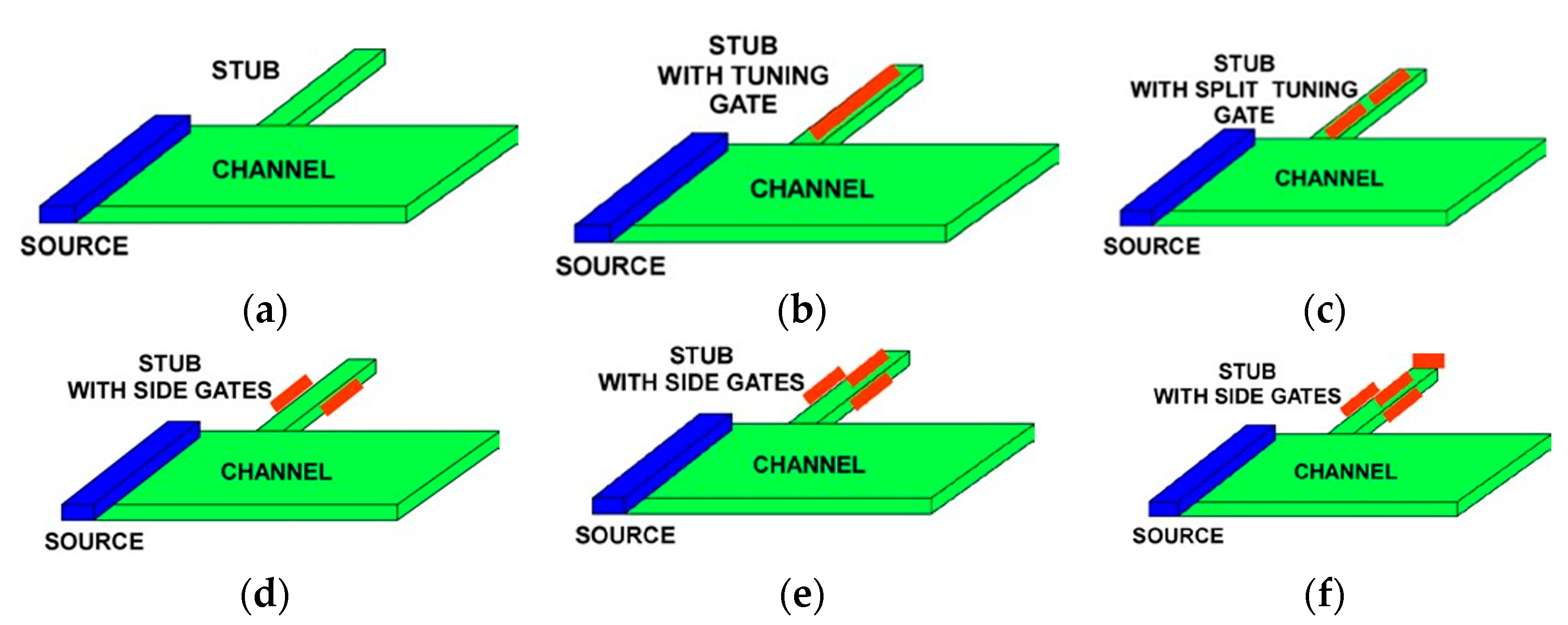
- Aizin, G.R.; Mikalopas, J.; Shur, M.S. Plasmons in Ballistic Nanostructures with Stubs: Transmission Line Approach. IEEE Trans. Electron. Devices 2018, 66, 126–131. [Google Scholar] [CrossRef]
- Muravjov, A.V.; Veksler, D.B.; Popov, V.V.; Polischuk, O.; Hu, X.; Gaska, R.; Pala, N.; Saxena, H.; Peale, R.E.; Shur, M.S. Temperature dependence of plasmonic terahertz absorption in grating-gate GaN HEMT structures. Appl. Phys. Lett. 2010, 96, 042105. [Google Scholar] [CrossRef] [Green Version]
- Otsuji, A.; Dubinov, V.; Ya Aleshkin, D.; Svintsov, M.; Ryzhii, S.; Boubanga Tombet, D.; Yadav, A.; Satou, V.; Mitin, M.S.; Shur, V.; et al. Graphene-based van der Waals heterostructures for emission and detection of terahertz radiation. In Proceedings of the SPIE 9856, Terahertz Physics, Devices, and Systems X: Advanced Applications in Industry and Defense, Baltimore, MD, USA, 29 April 2016; p. 985603. [Google Scholar] [CrossRef]
- Rodríguez-Vázquez, P.; Grzyb, J.; Sarmah, N.; Heinemann, B.; Pfeiffer, U.R. A 65 Gbps QPSK one meter wireless link operating at a 225–255 GHz tunable carrier in a SiGe HBT technology. In Proceedings of the IEEE Radio Wireless Symposium, Anaheim, CA, USA, 15–18 January 2018; pp. 146–149. [Google Scholar]
- Al-Eryani; Knapp, H.; Kammerer, J.; Aufinger, K.; Li, H.; Maurer, L. Fully integrated single-chip 305–375-GHz transceiver with on-chip antennas in SiGe BiCMOS. IEEE Trans. Terahertz Sci. Technol. 2018, 8, 329–339. [Google Scholar] [CrossRef]
- Lisauskas, A.; Rämer, A.; Burakevič, M.; Chevtchenko, S.A.; Krozer, V.; Heinrich, W.; Roskos, H.G. Terahertz emission from biased AlGaN/GaN high-electron-mobility transistors. J. Appl. Phys. 2019, 125, 151614. [Google Scholar] [CrossRef]
- Wang, Z.; Chiang, P.-Y.; Nazari, P.; Wang, C.-C.; Chen, Z.; Heydari, P. A CMOS 210-GHz Fundamental Transceiver with OOK Modulation. IEEE J. Solid-State Circuits 2014, 49, 564–580. [Google Scholar] [CrossRef]
- Wang, C.; Lu, B.; Lin, C.; Chen, Q.; Miao, L.; Deng, X.; Zhang, J. 0.34-THz Wireless Link Based on High-Order Modulation for Future Wireless Local Area Network Applications. IEEE Trans. Terahertz Sci. Technol. 2014, 4, 75–85. [Google Scholar] [CrossRef]
- Sengupta, K.; Hajimiri, A. Distributed active radiation for THz signal generation. In Proceedings of the 2011 IEEE International Solid-State Circuits Conference, San Francisco, CA, USA, 20–24 February 2011; pp. 288–289. [Google Scholar]
- Sengupta, K.; Hajimiri, A. A 0.28 THz 4 x 4 power generation and beam-steering array. In Proceedings of the 2012 IEEE International Solid-State Circuits Conference, San Francisco, CA, USA, 19–23 February 2012; pp. 256–258. [Google Scholar]
- Available online: https://vadiodes.com/en/frequency-multipliers (accessed on 19 October 2021).
- Khalid, A.; Dunn, G.M.; MacPherson, R.F.; Thoms, S.; MacIntyre, D.; Li, C.; Steer, M.J.; Papageorgiou, V.; Thayne, I.G.; Kuball, M.; et al. Terahertz oscillations in an In0.53Ga0.47As submicron planar Gunn diode. J. Appl. Phys. 2014, 115, 114502. [Google Scholar] [CrossRef] [Green Version]
- Available online: https://terasense.com/products/ (accessed on 19 October 2021).
- Asada, M.; Suzuki, S. Terahertz Emitter Using Resonant-Tunneling Diode and Applications. Sensors 2021, 21, 1384. [Google Scholar] [CrossRef]
- Yadav, D.; Tamamushi, G.; Watanabe, T.; Mitsushio, J.; Tobah, Y.; Sugawara, K.; Dubinov, A.A.; Satou, A.; Ryzhii, M.; Ryzhii, V.; et al. Terahertz light-emitting graphene-channel transistor toward single-mode lasing. Nanophotonics 2018, 7, 741–752. [Google Scholar] [CrossRef]
- Boubanga-Tombet, S.A.; Satou, A.; Yadav, D.; But, D.B.; Knap, W.; Popov, V.V.; Gorbenko, I.V.; Kachorovskii, V.; Otsuji, T. Paving the Way for Tunable Graphene Plasmonic THz Amplifiers. Front. Phys. 2021, 9, 726806. [Google Scholar] [CrossRef]
- Gavrilov, N.G.; Knyazev, B.A.; Kolobanov, E.I. Status of the Novosibirsk high-power terahertz FEL. Nucl. Instrum. Methods Phys. Res. 2007, 575, 54–57. [Google Scholar] [CrossRef]
- He, W.; Zhang, D.L.; Bowes, H.; Yin, K.; Ronald, A.D.; Phelps, R.; Cross, A.W. Generation of broadband terahertz radiation using a backward wave oscillator and pseudospark-sourced electron beam. Appl. Phys. Lett. 2015, 107, 133501. [Google Scholar] [CrossRef]
- Development of MW & THz Klinotrons. Available online: http://ire.kharkov.ua/Mysite/HTML/p0019.htm (accessed on 19 October 2021).
- Thumm, M. State-of-the-Art of High-Power Gyro-Devices and Free Electron Masers. J. Infrared Millim. Terahertz Waves 2020, 41, 1–140. [Google Scholar] [CrossRef] [Green Version]
- de Maagt, P.; Bolivar, P.H.; Mann, C. Terahertz Science, Engineering and Systems—From Space to Earth Applications. Encycl. RF Microw. Eng. 2005. [Google Scholar] [CrossRef]
- Siegel, P.H. THz for space: The golden age. In Proceedings of the 2010 IEEE MTT-S International Microwave Symposium, Anaheim, CA, USA, 27 January 2010; pp. 816–819. [Google Scholar] [CrossRef]
- Xia, B.G.; Zhang, D.H.; Meng, J.; Huang, J.; Yao, C.F.; Zhang, J.S. Terahertz FSS for space borne passive remote sensing application. Electron. Lett. 2013, 49, 1398–1399. [Google Scholar] [CrossRef]
- Waters, J. Submillimeter-wavelength heterodyne spectroscopy and remote sensing of the upper atmosphere. Proc. IEEE 1992, 80, 1679–1701. [Google Scholar] [CrossRef]
- Shur, M.S. Terahertz Plasmonic Technology. IEEE Sens. J. 2021, 21, 12752–12763. [Google Scholar] [CrossRef]
- Akter, N.; Pala, N.; Knap, W.; Shur, M. Chapter 8: THz Plasma Field Effect Transistor Detectors, in Fundamentals of Terahertz Devices and Applications; Pavlidis, D., Ed.; Wiley: Hoboken, NJ, USA, 2021. [Google Scholar]
- Matsuura, Y.; Suzuki, T.; Katagiri, T. Terahertz gas sensing based on time-domain-spectroscopy using a hollow-optical fiber gas cell. Opt. Fibers Sens. Med. Diagn. Treat. Appl. XVIII 2018, 10488, 1048808. [Google Scholar] [CrossRef]
- Kiwa, T.; Kamiya, T.; Morimoto, T.; Fujiwara, K.; Maeno, Y.; Akiwa, Y.; Iida, M.; Kuroda, T.; Sakai, K.; Nose, H.; et al. Imaging of Chemical Reactions Using a Terahertz Chemical Microscope. Photonics 2019, 6, 10. [Google Scholar] [CrossRef] [Green Version]
- Yang, L.; Guo, T.; Zhang, X.; Cao, S.; Ding, X. Toxic chemical compound detection by terahertz spectroscopy: A review. Rev. Anal. Chem. 2018, 37, 410. [Google Scholar] [CrossRef]
- Chen, Y.; Liu, H.; Fitch, M.J.; Osiander, R.; Spicer, J.B.; Shur, M.; Zhang, X.C. THz Diffuse Reflectance Spectra of Selected Explosives and Related Compounds, Passive Millimeter-Wave Imaging Technology VIII; Roger, A., David, A.W., Eds.; International Society for Optics and Photonics: Bellingham, WA, USA, 2005; Volume 5790, pp. 19–24. [Google Scholar]
- Federici, F.; Schulkin, B.; Huang, F.; Gary, D.; Barat, R.; Oliveira, F.; Zimdars, D. THz imaging and sensing for security applications- explosives, weapons, and drugs. Semicond. Sci. Technol. 2005, 20, S266. [Google Scholar] [CrossRef]
- Zhong, H.; Karpowicz, N.; Xu, J.; Deng, Y.; Ussery, W.; Shur, M.; Zhang, X.-C. Inspection of space shuttle insulation foam defects using a 0.2 THz Gunn diode oscillator, Infrared and Millimeter Waves. In Proceedings of the 12th International Conference on Terahertz Electronics, Karlsruhe, Germany, 27 September 2004; pp. 753–754. [Google Scholar]
- Lee, E.S.; Moon, K.; Lee, I.M.; Park, D.W.; Choi, D.H.; Shin, J.H.; Kim, H.S.; Choi, D.H.; Park, K.H. Terahertz Non-destructive Testing Technology for Industrial Applications. Electron. Telecommun. Trends 2018, 33, 59–69. [Google Scholar]
- Ruengwaree, A.; Ghose, A.; Weide, J.; Kampa, G. Ultra-fast pulse transmitter for UWB microwave radar. In Proceedings of the European Radar Conference, Manchester, UK, 13–15 September 2006; IEEE: Piscataway, NJ, USA; pp. 354–357. [Google Scholar]
- Nguyen, C.; Han, J. Time-Domain Ultra-Wideband Radar, Sensor and Components: Theory, Analysis and Design; Springer Science & Business Media: Berlin/Heidelberg, Germany, 2014. [Google Scholar]
- Sun, Q.; He, Y.; Liu, K.; Fan, S.; Parrott, E.P.J.; Pickwell-MacPherson, E. Recent advances in terahertz technology for biomedical applications. Quant. Imaging Med. Surg. 2017, 7, 345–355. [Google Scholar] [CrossRef] [PubMed] [Green Version]
- Heilweil, E.; Plusquellic, D. Terahertz Spectroscopy of Biomolecules; CRC Press: Boca Raton, FL, USA, 2007; pp. 269–297. [Google Scholar]
- Shur, M.S. Subterahertz and terahertz sensing of biological objects and chemical agents. Terahertz RF Millim. Submillim.-Wave Technol. Appl. XI 2018, 10531, 1053108. [Google Scholar] [CrossRef]
- Siegel, P.H. Terahertz Technology in Biology and Medicine. IEEE Trans. Microw. Theory Tech. 2004, 52, 2438–2447. [Google Scholar] [CrossRef]
- Hintzsche, H.; Jastrow, C.; Kleine-Ostmann, T.; Kärst, U.; Schrader, T.; Stopper, H. Terahertz Electromagnetic Fields (0.106 THz) Do Not Induce Manifest Genomic Damage In Vitro. PLoS ONE 2012, 7, e46397. [Google Scholar] [CrossRef]
- Yu, C.; Fan, S.; Sun, Y.; Pickwell-MacPherson, E. The potential of terahertz imaging for cancer diagnosis: A review of investigations to date. Quant. Imaging Med. Surg. 2012, 2, 33–45. [Google Scholar] [CrossRef]
- Farooq, M.; Shur, M. Inspection System and Method for Detecting Defects at a Materials Interface. U.S. Patent 10,215,695 Bl, 26 February 2019. [Google Scholar]
- Rupper, G.; Suarez, J.; Rudin, S.; Reed, M.; Shur, M. Terahertz Plasmonics for Testing Very Large-Scale Integrated Circuits under Bias. U.S. Patent 10,890,618 B2, 12 January 2021. [Google Scholar]
- Shur, M.; Rudin, S.; Rupper, G.; Reed, M.; Suarez, J. Sub-terahertz testing of millimeter wave Monolithic and very large scale integrated circuits. Solid-State Electron. 2019, 155, 44–48. [Google Scholar] [CrossRef]
- Akter, N.; Karabiyik, M.; Shur, M.; Suarez, J.; Pala, N. AI Powered THz VLSI Testing Technology. In Proceedings of the 2020 IEEE 29th North Atlantic Test Workshop (NATW), Albany, NY, USA, 18–20 May 2020; pp. 1–5. [Google Scholar] [CrossRef]
- Akter, N.; Siddiquee, M.R.; Shur, M.; Pala, N. AI-Powered Terahertz VLSI Testing Technology for Ensuring Hardware Security and Reliability. IEEE Access 2021, 9, 64499–64509. [Google Scholar] [CrossRef]
- Shur, M.S.; Suarez, J. Nanoscale silicon MOSFET response to THz radiation for testing VLSI. In Proceedings of the 2018 IEEE 27th North Atlantic Test Workshop (NATW), Essex, VT, USA, 7–9 May 2018; pp. 1–6. [Google Scholar] [CrossRef]
- Deng, Y.; Shur, M.S. Electron mobility and terahertz detection using silicon MOSFETs. Solid-State Electron. 2003, 47, 1559–1563. [Google Scholar] [CrossRef]
- Available online: https://terasense.com/products/sub-thz-imaging-cameras/ (accessed on 11 November 2011).
- Shur, M. AlGaN/GaN plasmonic terahertz electronic devices. J. Phys. 2014, 486, 012025. [Google Scholar] [CrossRef]
- Ahi, K. Review of GaN-based devices for terahertz operation. Opt. Eng. 2017, 59, 090901. [Google Scholar] [CrossRef]


| Detector Type | Frequency (THz) | Noise Equivalent Power (pW/Hz1/2) |
|---|---|---|
| AlGaN/GaN TeraFETs | 0.49–0.65 | 25–31 |
| AlGaN/GaN TeraFETs | 0.7–0.9 | 30–50 |
| 65 nm Si CMOS | 0.8–1 | 100 |
| 65 nm Si CMOS | 0.65 | 17 |
| 65 nm Si CMOS | 0.72 | 14 |
| 90 nm Si CMOS | 0.6 | 48–70 |
| 130 nm Si CMOS | 0.26 | 8.4 |
| THz Detector | Mechanism | Speed | Operating Temperature (K) | Responsivity (kV/W or A/W) | NEP (pW/Hz−1/2) |
|---|---|---|---|---|---|
| Golay cell | Thermal | Slow | 300 | 10–100 kV/W | ~100 |
| Bolometer | Thermal | Slow | 4.2 | ~100 kV/W | ~0.1 |
| Schottky diode | Rectification | Fast | 300 | 0.1 to 1.5 kV/W | 2.7 to 40 |
| GaN TeraFET | Plasmonic | Fast | 300 | 1.1 kV/W | 40 |
| Grated Gate TeraFET | Plasmonic | Fast | 300 | 2.2 to 23 kV/W | 0.5 to 50 |
| Resonant tunnelling diode | Resonant tunnelling | Fast | 300 | 7.3 A/W | 7.7 |
| Resonant tunnelling diode | Resonant tunnelling | Fast | 300 | 0.9 kV/W | 2.5 |
| THz Emitter | Frequency (THz) | Output Power (mW) 300 K | DC Power (mW) | Efficiency (%) | Reference |
|---|---|---|---|---|---|
| 40 nm Si CMOS | 0.266 | 0.69 | 1790 | 0.039 | [7] |
| GaAs pHEMT | 0.144–0.432 | 0.063 @300 K 0.278 @77 K | 180 (estimated) | 0.1 | [60] |
| 130 nm SiGe HBTs | 0.25 | 7.08 | 1960 | 0.36 | [116] |
| 130 nm SiGe BiCMOS | 0.34 | 1.02 | 1700 | 0.87 | [117] |
| Schottky diode frequency multipliers | 0.05–520 | 1900–200 | - | 38–5 | [123] |
| Gunn diodes | 0.1–0.3 | 0.05–0.023 | - | - | [124] |
| IMPATT diodes | 0.1–300 | 400–10 | - | - | [125] |
| Resonant tunnelling diode array | 1–1.98 | 0.7 | - | - | [126] |
| THz plasmon-emitting graphene-channel transistor | 1–7.6 | 0.01 @5.2 THz 0.001 @7.6 THz @100 K | - | - | [127] |
Publisher’s Note: MDPI stays neutral with regard to jurisdictional claims in published maps and institutional affiliations. |
© 2021 by the authors. Licensee MDPI, Basel, Switzerland. This article is an open access article distributed under the terms and conditions of the Creative Commons Attribution (CC BY) license (https://creativecommons.org/licenses/by/4.0/).
Share and Cite
Shur, M.; Aizin, G.; Otsuji, T.; Ryzhii, V. Plasmonic Field-Effect Transistors (TeraFETs) for 6G Communications. Sensors 2021, 21, 7907. https://doi.org/10.3390/s21237907
Shur M, Aizin G, Otsuji T, Ryzhii V. Plasmonic Field-Effect Transistors (TeraFETs) for 6G Communications. Sensors. 2021; 21(23):7907. https://doi.org/10.3390/s21237907
Chicago/Turabian StyleShur, Michael, Gregory Aizin, Taiichi Otsuji, and Victor Ryzhii. 2021. "Plasmonic Field-Effect Transistors (TeraFETs) for 6G Communications" Sensors 21, no. 23: 7907. https://doi.org/10.3390/s21237907