1. Introduction
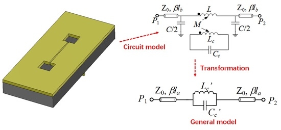
The dumbbell defect-ground-structure (DB-DGS) resonator [
1,
2] is a slot resonator exhaustively used in microwave engineering for the implementation of circuits (mainly filters [
3,
4,
5,
6,
7,
8,
9]) and sensors [
10,
11,
12,
13]. DB-DGS resonators are typically combined with microstrip transmission lines. The typical topology of a DB-DGS-loaded microstrip line is depicted in
Figure 1, where the resonant element is transversally etched in the ground plane. This structure exhibits a notched response with a transmission zero at the fundamental resonance frequency of the DB-DGS resonator, and the structure has been typically modelled by means of a parallel resonant tank series-connected to the host transmission line [
1,
2] (see
Figure 1b).
The notched response of DB-DGS-loaded microstrip lines can be exploited for the implementation of notch and stopband filters [
3,
4,
5,
6], as well as for the design of common-mode filters in differential lines [
7,
9]. However, slot resonators, including the DB-DGS resonator, are also of interest for the implementation of planar microwave sensors devoted to permittivity measurements, and to the characterization of materials (including solids and liquids) [
10,
11,
12,
13]. The reason is that the resonance frequency of these slot resonators is very sensitive to the dielectric properties of the material surrounding the resonator (in contact or in close proximity to it). Thus, the canonical output variable in these permittivity sensors is the resonance frequency of the resonant element (and eventually the notch magnitude) very sensitive to the permittivity of the so-called material under test (MUT).
For both circuit and sensor design, accurate circuit models of the structures under consideration (able to link the geometry parameters to the lumped elements of the model) are very convenient. As mentioned, the most accepted circuit model of a DB-DGS-loaded microstrip line is the one depicted in
Figure 1b, where the DB-DGS resonator is modelled by means of the parallel resonant tank, series connected to the line. It has been argued that this model accounts for the return current path in the ground plane, either across the narrow slot of the DB-DGS resonator (providing the capacitive effect), or surrounding the apertures (inductive effect) [
1,
2,
9]. Thus, according to this physical interpretation, the parallel combination of the inductance and the capacitance of the DB-DGS, as well as the connection of this parallel LC tank in series with the line, is clear. However, the fact that the resonator is etched in the ground plane generates some doubts concerning the validity of the above-mentioned physical interpretation of the model parameters. Indeed, in microstrip-to-slot-line transitions, it has been reported that the excitation of the slot line is due to magnetic coupling [
14,
15]. In the structure of
Figure 1, rather than a microstrip-to-slot-line transition, a microstrip line excites a slot resonator with apertures in the extremes, i.e., a DB-DGS resonator. However, it is apparent that the driving mechanism should be the same. Indeed, in previous papers [
16,
17], a different model of the DB-DGS-loaded microstrip line, which accounts for the magnetic coupling between the host line and the resonant element, has been reported. Actually, the simple model of
Figure 1 can be derived from such model by element transformation. However, the interpretation of the elements of the parallel resonant tank of
Figure 1, as those describing the capacitance and inductance of the DB-DGS resonator, does not seem to be correct or, at least, accurate. In this paper, all these aspects are discussed in detail, and the implications on the functionality of the DB-DGS-loaded line as permittivity sensor are analyzed.
2. Model and Analysis
Any planar microwave resonator, including both metallic and slot-based resonators, can be modelled by means of a LC resonant tank in the vicinity of the fundamental resonance. Additionally, if the considered resonator is electrically small, then the LC resonant tank provides a good description of the resonant element in a relatively broad band that extends significantly above the fundamental resonance. The DB-DGS resonator is the complementary, or dual, counterpart of the so-called step-impedance-resonator (SIR) [
18,
19]. Thus, likewise the SIR, the DB-DGS resonator can be considered an electrically small resonator, by virtue of the high contrast between the width of the narrow (central) slot and the apertures at the extremes. Whereas in the SIR the inductance is mainly due to the narrow strip and the capacitance to the metallic patches at the extremes [
18,
19], it follows from duality considerations [
20,
21,
22] that the narrow slot of the DB-DGS resonator determines its capacitance, whilst the inductance is mainly determined by the size of the apertures. However, in the model depicted in
Figure 1b, the reactive element values
Lc′ and
Cc′ are not the inductance and capacitance, respectively, of the DB-DGS resonator. Nevertheless, as it will be shown later,
Lc′ and
Cc′ are related to the inductance
Lc and capacitance
Cc, respectively, of the DB-DGS resonator.
At the fundamental resonance frequency, a DB-DGS resonator exhibits a magnetic wall at its symmetry plane (the axis of the microstrip line in
Figure 1a). Consequently, the fundamental resonance of the DB-DGS resonator can be driven by means of a time-varying magnetic field with a non-negligible component in the plane of the particle, in the direction orthogonal to the magnetic wall. It is obvious that the magnetic field generated by the line satisfies such requirement. Therefore, the line present on top of the DB-DGS can magnetically excite the resonant element. Thus, a more realistic circuit model of the DB-DGS-loaded microstrip transmission line is the one depicted in
Figure 2a [
16,
17]. In this model,
Lc and
Cc describe the DB-DGS resonator, as indicated before. Particularly, the capacitance
Cc is determined by the length and width of the narrow (central) slot, whereas the size of the apertures is the main parameter determining the inductance value
Lc. In order to describe the magnetic coupling between the microstrip line and the resonator, we should model a portion of the line (with length
l, where
l <
la) by means of its inductance
L and capacitance
C. By this means, we can define a mutual inductance
M, describing the magnetic coupling between the line and the DB-DGS resonator. In coherence with
Figure 1, the length of the transmission line sections in
Figure 2 is simply
lb =
la −
l/2.
The series branch in the circuit of
Figure 2a can be transformed to a parallel resonator series-connected to an inductor (
Figure 2b). The elements of the series branch in the circuit of
Figure 2b are related to the elements of the original circuit of
Figure 2a through the following equations [
17,
22]
where
=
(
being the angular frequency at the fundamental resonance of the DB-DGS resonator). If we compare the circuit of
Figure 2b with the one in
Figure 1b, the difference is the presence of the inductance
L′ and the capacitance
C in the circuit of
Figure 2b, not present in the circuit of
Figure 1b. However, as it will be later demonstrated,
L′ and
C describe the transmission line section of length
l. Such line section, plus the lines of length
lb in the circuit of
Figure 2b, give the total line length
la of the circuit of
Figure 1b.
According to the preceding paragraph, the circuits of
Figure 1b and
Figure 2b or
Figure 2a, are effectively equivalent, and, therefore, it is licit to consider valid the circuit of
Figure 1b. However, in the circuit of
Figure 1b, the reactive elements
Lc′ and
Cc′ do not correspond to the inductance and capacitance of the DB-DGS resonator, as anticipated before. Nevertheless, the reactive elements of the resonators in both models (
Figure 2a,b) are intimately related. By introducing
in Equations (2) and (3) one obtains:
providing the relationship between the resonator elements in both models. Note, however, that there is a fundamental difference between the models of
Figure 2a,b. Whereas the series branch in the model of
Figure 2a depends on four reactive parameters (
L,
M,
Lc and
Cc), the series branch in the circuit model of
Figure 2b, equivalent to
Figure 1b, contains only three reactive elements (
L′,
Lc′ and
Cc′). Thus, from the information of the reactive parameters of the circuit of
Figure 2b, easily obtained from parameter extraction [
22,
23,
24], it is not possible to obtain
M,
Lc and
Cc. By contrast,
L can be easily isolated from Equation (1). In order to independently obtain
M,
Lc and
Cc from
Lc′ and
Cc′, at least one of the three reactive parameters
M,
Lc or
Cc must be determined from an independent method. Let us discuss this aspect in the next section, where the implications of the transformation Equations (1)–(3) or Equations (4) and (5), on the functionality of the DB-DGS-loaded line as permittivity sensor are discussed.
3. Parametric Analysis and Implications for Permittivity Sensing
Let us consider as case study a microstrip transmission line loaded with a DB-DGS resonator with the dimensions depicted in the caption of
Figure 3, where the specific topology is depicted. The width of the line (
W = 1.1 mm) provides a 50-Ω characteristic impedance with the considered substrate parameters (dielectric constant
εr = 10.2 and thickness
h = 1.27 mm). The response of this structure inferred from electromagnetic simulation is depicted in
Figure 3b. From this response, we have extracted the parameters of the circuit of
Figure 2b, i.e.,
L′ = 5.12 nH,
Lc′ = 4.10 nH,
Cc′ = 3.63 pF and
C = 2.21 pF (the parameter extraction method reported in [
22,
23,
24] has been used). Actually, such parameters correspond to the DB-DGS coupled to a line section of length
l = 12 mm (note that the obtained values of
L′ and
C are compatible with a 50-Ω characteristic impedance line of the considered length, i.e., 12 mm). With such parameters, the circuit response is found to be roughly undistinguishable from the electromagnetic response in the considered frequency range. However, as mentioned, it is not possible to infer
M,
Lc and
Cc by means of Equations (1)–(3), or Equations (4) and (5). In the circuit of
Figure 2a, only the capacitance
C, invariable as compared to the one of
Figure 2b, and
L (=
L′+
Lc′ = 9.21 nH), can be univocally determined.
In order to be able to obtain the circuit parameters of the original model of
Figure 2a, we have considered an auxiliary structure, i.e., a microstrip line loaded with an identical DB-DGS resonator, but folded and rotated 90°, as depicted in
Figure 4 (this structure can also be useful for permittivity sensing). In this structure, the magnetic coupling cancels because the symmetry plane of the particle, a magnetic wall, is orthogonally oriented with regard to the line axis. However, there is an electric dipole in the vertical direction, since the resonator is folded [
17]. Therefore, with such orientation and folding, the DB-DGS resonator is excited exclusively by the electric field generated by the line, with a significant component in the vertical direction. The circuit model for this structure is thus the one shown in
Figure 5. The parameters of this model can be easily extracted (the method reported in [
23] has been applied), and the results are as follows:
L″ = 9.27 nH,
C″ = 2.07 pF,
Cc″ = 4.23 pF and
Lc″ = 3.68 nH (the electromagnetically simulated and circuit response are depicted in
Figure 4b). As it can be appreciated,
L″ ≈
L and
C″ ≈
C, i.e., the parameters describing the line section of length
l do not appreciable change by rotating and folding the DB-DGS resonator. In this paper, we do assume that the capacitance
Cc of the unfolded DB-DGS does not change as compared to the one of the folded particles,
Cc″. This latter hypothesis is reasonable, since the capacitance of the resonator mainly depends on the length and width of the narrow (central) slot and it is not expected that such capacitance varies significantly by rotating and folding the DB-DGS. By considering that
Cc″ =
Cc, the remaining parameters of the circuit of
Figure 2a, i.e.,
M and
Lc, can be perfectly determined from inversion of Equations (4) and (5), or Equations (1)–(3), and the results are
M = 3.80 nH and
Lc = 3.52 nH. Let us clarify that in the circuit of
Figure 5, the capacitance
Cc″ can be univocally determined from parameter extraction. However, from the extracted parameters of the circuit of
Figure 2b, it is not possible through inversion of Equations (4) and (5) or Equations (1)–(3), to univocally determining the elements of the series branch in the circuit of
Figure 2a, particularly
M,
Lc and
Cc. It is neither possible to infer these elements from direct parameter extraction, since, given a response, for example the one of
Figure 3b, corresponding to the structure of
Figure 3a, there are many combinations of the triad
M,
Lc and
Cc providing such response, as inspection of Equations (1)–(3) and Equations (4) and (5) reveals.
Note that the inductance of the rotated and folded resonator varies slightly, as compared to the one of the unfolded and transversally oriented DB-DGS, i.e.,
Lc″ ≠
Lc. This is attributed to the fact that the current path from the inner to the outer metallic region of the folded particle is very different from the inductive current path in the unfolded resonator. Moreover, the influence of the line strip on the inductance of the DB-DGS is more severe if the particle is folded and oriented as shown in
Figure 4a.
To gain insight on the behavior of the reactive elements when dimensions are modified, we have considered variations in the length of the narrow slot of the DB-DGS (keeping the other dimensions unaltered). This should mainly (although not exclusively) affect the capacitance of the resonant particle, and it is reasonable to consider the effects of varying such dimension. The reason is that in the functionally of the structure under consideration as permittivity sensor, the material under test (MUT), placed on top of the DB-DGS, modifies the capacitance of the particle. Nevertheless, it should be mentioned that it is also expected that the inductance of the particle, Lc, as well as the mutual inductance, M, experience a certain variation by varying the length of the narrow slot of the DB-DGS resonators. By contrast, such inductive elements are not altered by the presence of a dielectric material (MUT) on top of the DB-DGS.
Figure 6 depicts the electromagnetically simulated responses that are obtained by varying the slot length in a quantity Δ
l as compared to the nominal value. As expected, the resonance frequency decreases with the slot length. The extracted parameters of the circuit of
Figure 2b are shown in
Table 1. The circuit responses inferred from the extracted parameters for each case are also depicted in
Figure 6 for comparison purposes, and the agreement is good in all the cases. By applying the previous procedure, the parameters of the model of
Figure 2a have been obtained, and the results are also depicted in
Table 1. The capacitance of the resonator,
Cc, and the transformed capacitance,
Cc′, both increase with the slot length, as expected, but it can be seen that
Lc,
Lc′ and
M experience an appreciable variation, as well. The important aspect of this analysis is that
Cc and
Cc′ increase with the slot length. However, the capacitance that has a physical interpretation, i.e., the one of the DB-DGS resonator (attributed to the narrow slot), is
Cc, rather than
Cc′.
Let us next consider the effects of varying the capacitance of the DB-DGS resonator, but rather than by tailoring particle dimensions (narrow slot length), by covering the DB-DGS by means of a dielectric MUT with semi-infinite length in the vertical direction, and with lateral dimensions extending far beyond the boundaries of the DB-DGS (semi-infinite approximation). This approximation, which means that the electric field generated by the DB-DGS does not reach the limits of the MUT, is not a sensor requirement. However, it eases the analysis, to be carried out later, and does not represent a loss of generality. The responses of the DB-DGS-loaded line with nominal dimensions (i.e., with narrow slot length 2
l = 24 mm) for MUTs with various dielectric constant are depicted in
Figure 7a. By covering the DB-DGS with a dielectric material,
Cc should change, but not
Lc and
M, as indicated before. Consequently, according to Equations (4) and (5),
Cc′ should vary with the dielectric constant of the MUT, but not
Lc′. If we infer the circuit responses for the different dielectric constant of the MUT using the different values of
Cc′ that are required to adjust the resonance frequency to the simulated value (keeping the other parameters invariable), the agreement with the simulations is very good. The values of
Cc′ and
Cc for the different dielectric constants are shown in
Table 2. Let us call
Cc,air the value of
Cc corresponding to the DB-DGS surrounded by air (with dielectric constant
εMUT = 1). For a semi-infinite MUT with arbitrary dielectric constant, the capacitance of the resonator should vary according to [
25,
26]
where
is the so-called equivalent dielectric constant of the substrate, defined in [
26], which takes into account the finite thickness of the substrate. Namely, if the substrate satisfies the semi-infinite approximation, the capacitance
Cc is given by (6) with
replaced with
, the substrate dielectric constant [
25,
26]. However, if the field lines generated in the slot of the DB-DGS resonator reach the opposite substrate interface, then the capacitance should be calculated according to (6). Equation (6) assumes that the capacitance of the resonator
Cc is given by the parallel combination of the capacitances of the upper (MUT) and lower (substrate) subspaces of the slot, a hypothesis that is valid provided there is a quasi-magnetic wall in the plane of the DB-DGS resonator. In [
26], it was demonstrated that for any reasonable combination of substrate thickness, substrate dielectric constant, and slot width, it can be considered that the plane of the particle is a magnetic wall to a very good approximation, thereby pointing out the validity of (6). The physical interpretation of
is clear, namely, it is the value of the dielectric constant that a hypothetical semi-infinite substrate should exhibit in order to provide a contribution to the capacitance of the particle identical to the one of the actual (finite) substrate. The method for the calculation of
is simple. Let us call
f0,air and
f0,MUT the resonance frequencies of the DB-DGS resonator when it is unloaded and loaded with a certain (semi-infinite) MUT, respectively. The ratio of these frequencies is
Provided the inductance of the DB-DGS resonator does not vary with the presence of the MUT. Since these frequencies can be easily obtained from electromagnetic simulation, it follows that can be inferred from (7). The calculated value is = 6.30. Obviously, does not depend on the MUT. It only depends on the characteristics of the substrate and slot width. Thus, the value of should be the same, regardless of the considered value of the dielectric constant of the MUT, . This aspect has been corroborated by considered different values, providing roughly identical values of (not shown). Indeed, the value of given above is an average value, but the standard deviation is very small.
The capacitance values given by (6) are also included in
Table 2 and are very close to the values of
Cc inferred by inversion of (4–5) using the values of
Cc′ adjusted to fit the resonance values of the different MUTs. The circuit responses with the values of
Cc calculated by means of (6) are compared to the simulated responses in
Figure 7b, and the agreement is also very good.
From (4–5), it follows that
Cc′ should exhibit a dependence with
εMUT given by
Thus, if we call
, it is clear that the capacitance of the model of
Figure 2b has a dependence on
εMUT identical to the one of the capacitance of the circuit of
Figure 2a, the actual capacitance of the DB-DGS resonator. Moreover, the resonance frequency is identical in both models. Therefore, it is obvious that the sensitivity does not depend on whether the circuit model of
Figure 2b or the more realistic model of
Figure 2a is considered.
To gain more insight on this latter aspect, let us calculate the sensitivity, namely, the variation experienced by the output variable, the resonance frequency, with the input variable, the dielectric constant of the MUT, i.e.,
If the model of
Figure 2b is considered, the previous expression can be decomposed in two terms as follows
where the first and second terms are given by
and
respectively. Introducing (11) and (12) in (10), and using (8), the sensitivity is found to be
Alternatively, if the model of
Figure 2a is the considered one, the sensitivity is also given by (10), with
Cc′ replaced with
Cc. Equations (11) and (12) are also valid with
Cc′ replaced with
Cc, and
replaced with
. Note, however, that the resulting sensitivity is also given by (13), since the resonance frequency is identical in both models (see Equations (1)–(3). Therefore, according to this analysis, it can be unequivocally concluded that despite the fact that the capacitance
Cc′ does not correspond to the capacitance of the DB-DGS resonator, using the model of
Figure 2b for design purposes, as usually done with an eye towards simplification, is perfectly licit.
The sensitivity given by (13) is compared with the sensitivity inferred from the simulated data (resonances) of
Figure 7, and the agreement is very good, as shown in
Figure 8. This points out the validity of the previous sensitivity analysis. Note, however, that inferring the sensitivity from experimental results is difficult due to the lack of data points. Namely, the number of potential samples with different dielectric constant is limited. Nevertheless, we have experimentally validated the reported circuit models by covering the sensor structure of
Figure 3 with various semi-infinite materials, particularly uncladded substrates available in our laboratory.
Figure 9 depicts the response for such materials (indicated), and the agreement between experimental, circuit and electromagnetic simulation is good. Small discrepancies are due to fabrication related tolerances, and to the fact that the samples are actually stacked slabs, with certain air gap effect between them (there are not thick enough substrates so as to consider them semi-infinite).


