
A Novel Approach for the Creation of Electrically Controlled LC:PDMS Microstructures

 ,
,  , ,
, ,
Abstract
:1. Introduction
2. Materials and Methods
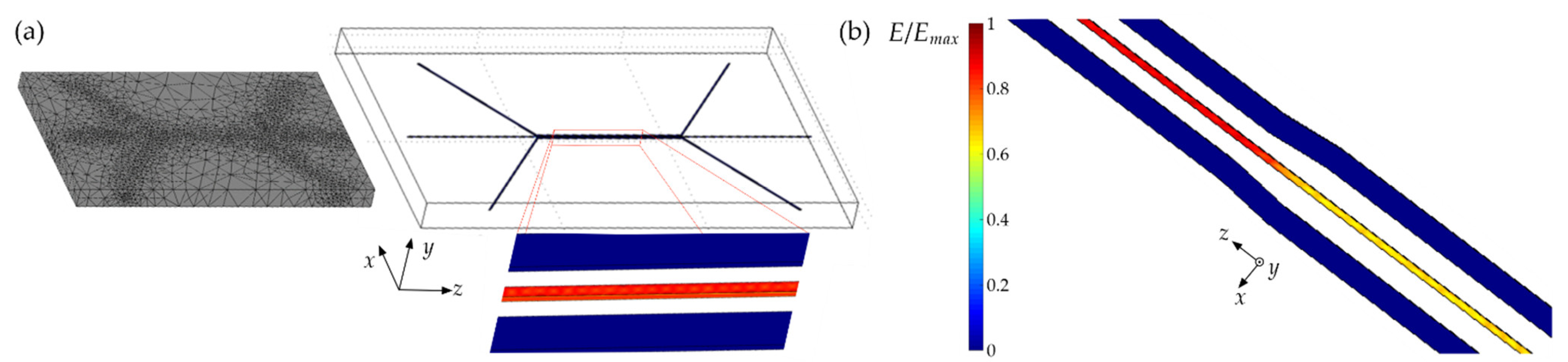
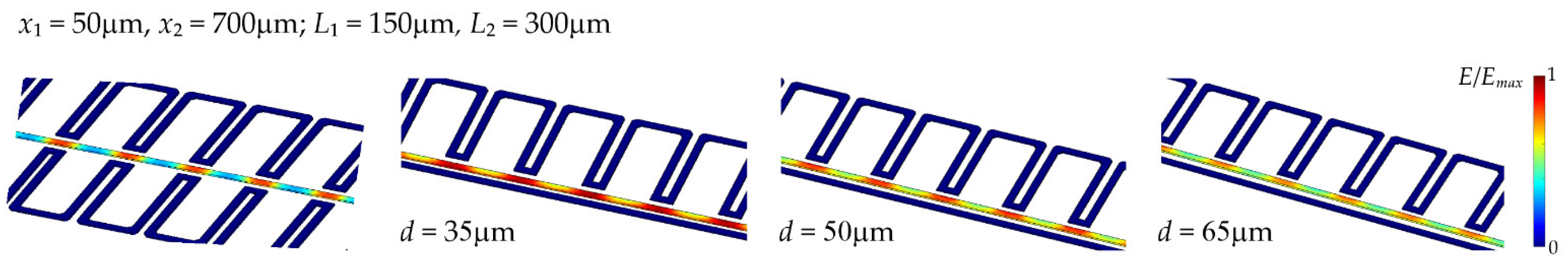
2.1. Numerical Modelling Methods
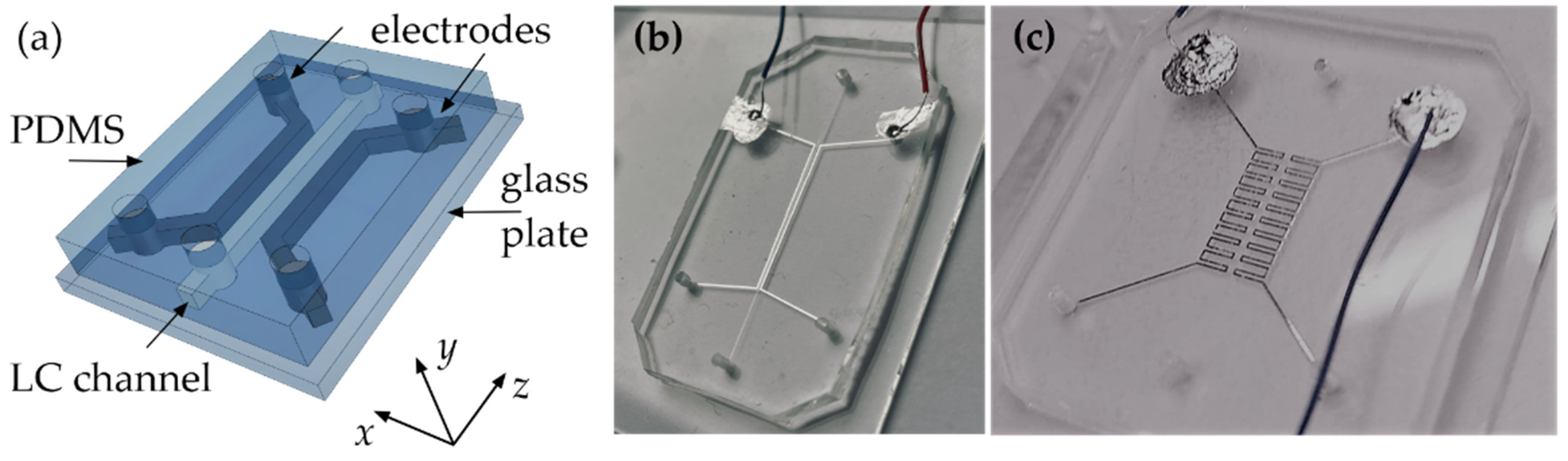
2.2. Fabrication of LC:PDMS Microstructures
2.3. Testing the Influence of an Electric Field on LC Molecular Orientation
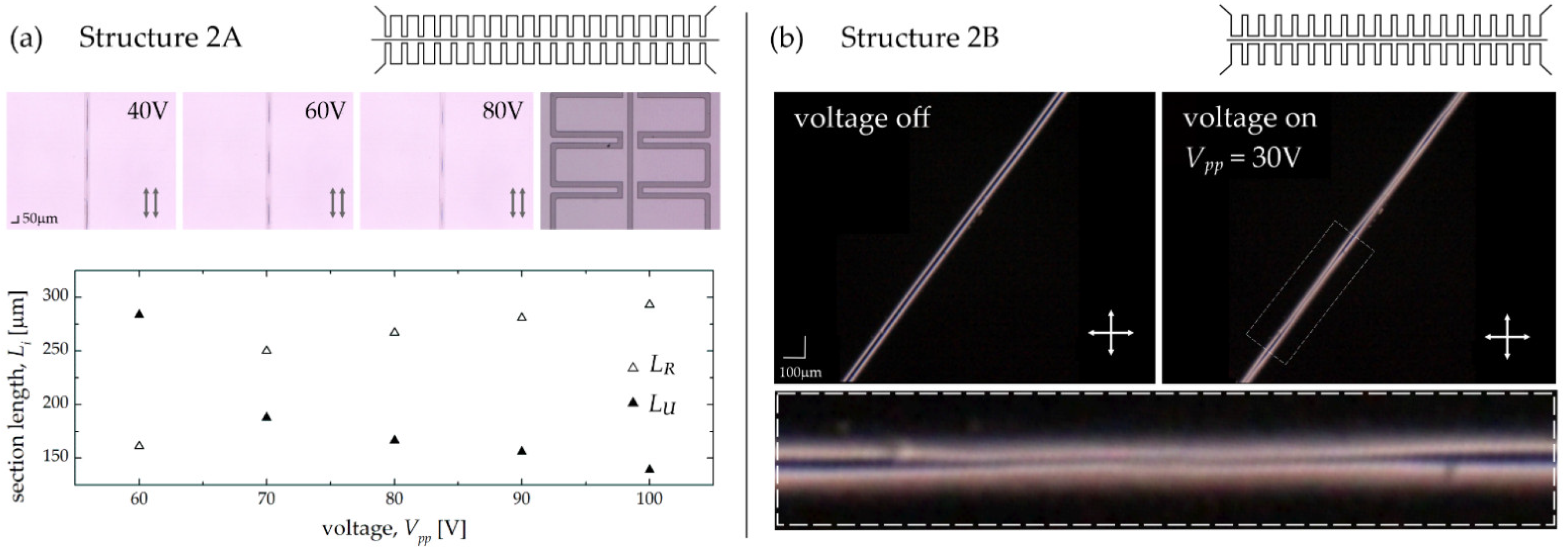
3. Results
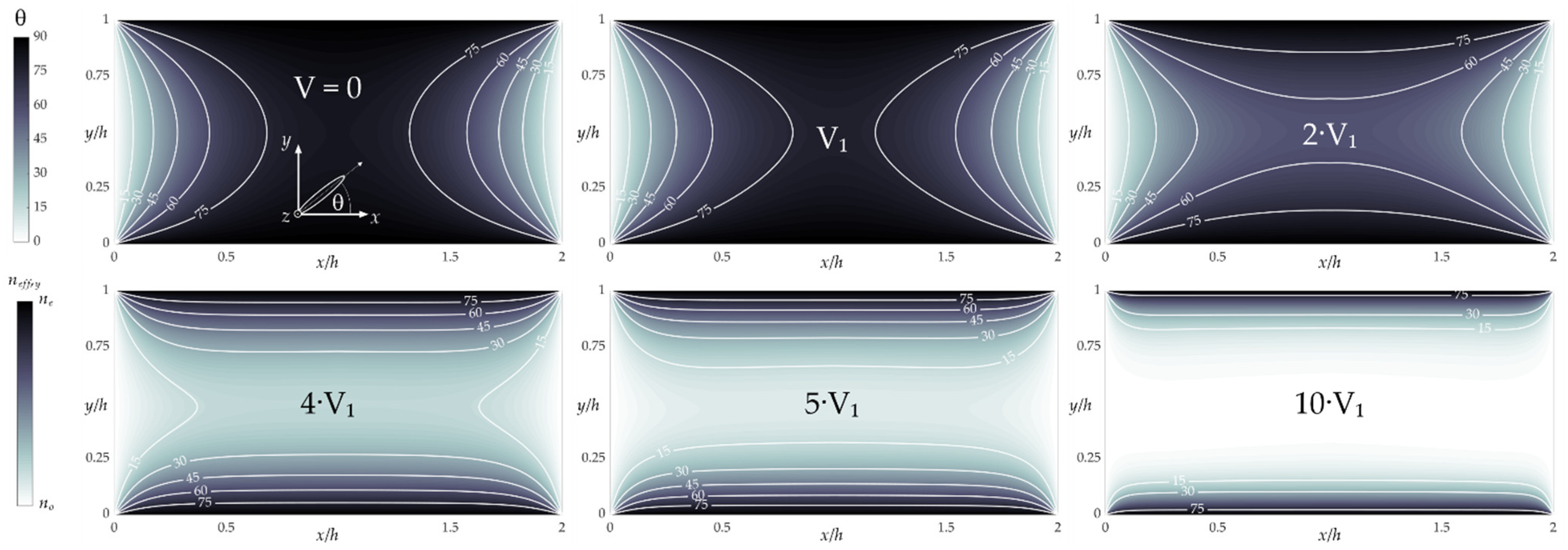
3.1. Results of Numerical Simulations
3.2. Experimental Results
4. Conclusions
Author Contributions
Funding
Conflicts of Interest
References
- Fainman, Y.; Lee, L.; Psaltis, D.; Yang, C. Optofluidics: Fundamentals, Devices, and Applications; McGraw-Hill, Inc.: New York, NY, USA, 2009. [Google Scholar]
- Raj, M.K.; Chakraborty, S. PDMS microfluidics: A mini review. J. Appl. Polym. Sci. 2020, 137, 48958. [Google Scholar] [CrossRef]
- Rabiee, N.; Ahmadi, S.; Fatahi, Y.; Rabiee, M.; Bagherzadeh, M.; Dinarvand, R.; Bagheri, B.; Zarrintaj, P.; Saeb, M.R.; Webster, T.J. Nanotechnology-assisted microfluidic systems: From bench to bedside. Nanomedicine 2020, 16, 237–258. [Google Scholar] [CrossRef] [PubMed]
- Verma, N.; Pandya, A. Challenges and opportunities in micro/nanofluidic and lab-on-a-chip. In Micro/Nanofluidics and Lab-on-Chip Based Emerging Technologies for Biomedical and Translational Research Applications—Part A; Academic Press: Cambridge, MA, USA, 2022; pp. 289–302. [Google Scholar]
- Samiei, E.; Tabrizian, M.; Hoorfar, M. A review of digital microfluidics as portable platforms for lab-on a-chip applications. Lab Chip 2016, 16, 2376–2396. [Google Scholar] [CrossRef] [PubMed]
- Quake, S.R.; Scherer, A. From micro-to nanofabrication with soft materials. Science 2000, 290, 1536–1540. [Google Scholar] [CrossRef] [PubMed] [Green Version]
- McDonald, J.C.; Whitesides, G.M. Poly (dimethylsiloxane) as a material for fabricating microfluidic devices. Acc. Chem. Res. 2002, 35, 491–499. [Google Scholar] [CrossRef]
- Karnutsch, C.; Tomljenovic-Hanic, S.; Monat, C.; Grillet, C.; Domachuk, P.; McPhedran, R.; Eggleton, B.J.; O’Faolain, L.; Krauss, T.F.; Xiao, S. Waveguide-based optofluidics. Proc. SPIE 2010, 7606, 760615. [Google Scholar]
- Monat, C.; Domachuk, P.; Eggleton, B.J. Integrated optofluidics: A new river of light. Nat. Photonics 2007, 1, 106. [Google Scholar] [CrossRef]
- The Dow Chemical Company. SYLGARD™ 184 Silicone Elastomer; Technical Data Sheet; The Dow Chemical Company: Midland, MI, USA, 2017. [Google Scholar]
- Murphy, E.C.; Dumont, J.H.; Park, C.H.; Kestell, G.; Lee, K.S.; Labouriau, A. Tailoring properties and processing of Sylgard 184: Curing time, adhesion, and water affinity. J. Appl. Polym. Sci. 2020, 137, 48530. [Google Scholar] [CrossRef]
- Silverio, V.; Silva, A.V.; Przykaza, K.; Santos, L.F.; Melo, L.V.; Cardoso, S. Dark matters: Black-PDMS nanocomposite for opaque microfluidic systems. Phys. Chem. Chem. Phys. 2019, 21, 2719–2726. [Google Scholar] [CrossRef]
- d’Alessandro, A.; Martini, L.; Civita, L.; Beccherelli, R.; Asquini, R. Liquid crystal waveguide technologies for a new generation of low-power photonic integrated circuits. Proc. SPIE 2015, 9384, 93840L. [Google Scholar]
- Rutkowska, K.A.; Woliński, T.R.; Asquini, R.; Civita, L.; Martini, L.; d Alessandro, A. Electrical tuning of the LC: PDMS channels. Photonics Lett. Pol. 2017, 9, 48–50. [Google Scholar] [CrossRef] [Green Version]
- d’Alessandro, A.; Asquini, R. Light Propagation in Confined Nematic Liquid Crystals and Device Applications. Appl. Sci. 2021, 11, 8713. [Google Scholar] [CrossRef]
- d’Alessandro, A.; Kumaran, A.M. Light confinement in liquid crystals for optofluidic integrated microsystems. In Proceedings of the EOS Annual Meeting (EOSAM 2021), Rome, Italy, 13–17 September 2021; p. 10001. [Google Scholar]
- d’Alessandro, A.; Civita, L.; Asquini, R.; Chiccoli, C.; Pasini, P. Optical waveguides and tunable devices made of a liquid crystal core in PDMS channels. Proc SPIE 2019, 11092, 110920W. [Google Scholar]
- Collings, P.J.; Goodby, J.W. Introduction to Liquid Crystals: Chemistry and Physics; CRC Press: Boca Raton, FL, USA, 2019. [Google Scholar]
- Baczyński, S.; Sobotka, P.; Marchlewicz, K.; Słowikowski, M.; Juchniewicz, M.; Dybko, A.; Rutkowska, K.A. Orientation of Liquid Crystalline Molecules on PDMS Surfaces and within PDMS Microfluidic Systems. Appl. Sci. 2021, 11, 11593. [Google Scholar] [CrossRef]
- Ahn, D.; Jeong, Y.-C.; Lee, S.; Lee, J.; Heo, Y.; Park, J.-K. Control of liquid crystal pretilt angles by using organic/inorganic hybrid interpenetrating networks. Opt. Express 2009, 17, 16603–16612. [Google Scholar] [CrossRef]
- Zheng, W.; Yang, L.; Lee, M. Vertical alignment of liquid crytals on polydimethylsiloxane thin films. Photonics Lett. Pol. 2011, 3, 8–10. [Google Scholar] [CrossRef]
- Zheng, W.J.; Huang, M.H. Use of polydimethylsiloxane thin film as vertical liquid crystal alignment layer. Thin Solid Film. 2012, 520, 2841–2845. [Google Scholar] [CrossRef]
- De Gennes, P.-G.; Prost, J. The Physics of Liquid Crystals; Clarendon Press Oxford: New York, NY, USA, 1993; Volume 23. [Google Scholar]
- Khoo, I.-C. Liquid Crystals: Physical Properties and Nonlinear Optical Phenomena; Wiley-VCH: Weinheim, Germany, 1994; p. 320. ISBN 0-471-30362-3. [Google Scholar]
- Blinov, L.M.; Chigrinov, V.G. Electrooptic Effects in Liquid Crystal Materials; Springer Science & Business Media: Berlin/Heidelberg, Germany, 1996. [Google Scholar]
- Babakhanova, G.; Lavrentovich, O.D. The techniques of surface alignment of liquid crystals. In Proceedings of the International Conference Physics of Liquid Matter: Modern Problems, Kyiv, Ukraine, 18–22 May 2018; pp. 165–197. [Google Scholar]
- Chigrinov, V.G.; Kozenkov, V.M.; Kwok, H.-S. Photoalignment of Liquid Crystalline Materials: Physics and Applications; John Wiley & Sons: Hoboken, NJ, USA, 2008; Volume 17. [Google Scholar]
- Kozanecka-Szmigiel, A.; Rutkowska, K.A.; Nieborek, M.; Kwasny, M.; Karpierz, M.A.; Schab-Balcerzak, E.; Konieczkowska, J.; Szmigiel, D. Photopatterned azo poly (amide imide) layers as aligning substrates of holographic liquid crystal diffraction gratings for beam steering applications. J. Mater. Chem. C 2020, 8, 968–976. [Google Scholar] [CrossRef]
- Sengupta, A. Topological Microfluidics: Nematic Liquid Crystals and Nematic Colloids in Microfluidic Environment; Springer Science & Business Media: Berlin/Heidelberg, Germany, 2013. [Google Scholar]
- Baek, S.-I.; Kim, S.-J.; Kim, J.-H. Measurement of anchoring coefficient of homeotropically aligned nematic liquid crystal using a polarizing optical microscope in reflective mode. AIP Adv. 2015, 5, 097170. [Google Scholar] [CrossRef]
- Li, G.; Qiu, Z.; Wang, Y.; Hong, Y.; Wan, Y.; Zhang, J.; Yang, J.; Wu, Z.; Hong, W.; Guo, C.F. PEDOT: PSS/grafted-PDMS electrodes for fully organic and intrinsically stretchable skin-like electronics. ACS Appl. Mater. Interfaces 2019, 11, 10373–10379. [Google Scholar] [CrossRef]
- Kayser, L.V.; Lipomi, D.J. Stretchable conductive polymers and composites based on PEDOT and PEDOT: PSS. Adv. Mater. 2019, 31, 1806133. [Google Scholar] [CrossRef] [PubMed] [Green Version]
- Baëtens, T.; Pallecchi, E.; Thomy, V.; Arscott, S. Cracking effects in squashable and stretchable thin metal films on PDMS for flexible microsystems and electronics. Sci. Rep. 2018, 8, 9492. [Google Scholar] [CrossRef] [PubMed] [Green Version]
- Al Mamun, N.H.; Dutta, P. Patterning of platinum microelectrodes in polymeric microfluidic chips. J. Micro/Nanolithogr. MEMS MOEMS 2006, 5, 039701. [Google Scholar] [CrossRef]
- Seghir, R.; Arscott, S. Controlled mud-crack patterning and self-organized cracking of polydimethylsiloxane elastomer surfaces. Sci. Rep. 2015, 5, 14787. [Google Scholar] [CrossRef]
- Sondhi, K.; Hwangbo, S.; Yoon, Y.-K.; Nishida, T.; Fan, Z.H. Airbrushing and surface modification for fabricating flexible electronics on polydimethylsiloxane. J. Micromech. Microeng. 2018, 28, 125014. [Google Scholar] [CrossRef]
- De Sio, L.; Romito, M.; Giocondo, M.; Vasdekis, A.E.; De Luca, A.; Umeton, C. Electro-switchable polydimethylsiloxane-based optofluidics. Lab Chip 2012, 12, 3760–3765. [Google Scholar] [CrossRef] [PubMed]
- Romito, M.; De Sio, L.; Vasdekis, A.E.; Umeton, C. Optofluidic microstructures containing liquid crystals. Mol. Cryst. Liq. Cryst. 2013, 576, 135–140. [Google Scholar] [CrossRef]
- Palermo, G.; De Sio, L.; Umeton, C. Flexible structures based on a short pitch cholesteric liquid crystals. Mol. Cryst. Liq. Cryst. 2015, 619, 35–41. [Google Scholar] [CrossRef]
- Casper, M.D.; Gözen, A.Ö.; Dickey, M.D.; Genzer, J.; Maria, J.-P. Surface wrinkling by chemical modification of poly (dimethylsiloxane)-based networks during sputtering. Soft Matter 2013, 9, 7797–7803. [Google Scholar] [CrossRef]
- Ko, E.-H.; Kim, H.-J.; Lee, S.-M.; Kim, T.-W.; Kim, H.-K. Stretchable Ag electrodes with mechanically tunable optical transmittance on wavy-patterned PDMS substrates. Sci. Rep. 2017, 7, 46739. [Google Scholar] [CrossRef]
- Kim, S.-R.; Kim, J.-H.; Park, J.-W. Wearable and transparent capacitive strain sensor with high sensitivity based on patterned Ag nanowire networks. ACS Appl. Mater. Interfaces 2017, 9, 26407–26416. [Google Scholar] [CrossRef] [PubMed]
- Wu, W.-Y.; Zhong, X.; Wang, W.; Miao, Q.; Zhu, J.-J. Flexible PDMS-based three-electrode sensor. Electrochem. Commun. 2010, 12, 1600–1604. [Google Scholar] [CrossRef]
- Bai, H.-J.; Shao, M.-L.; Gou, H.-L.; Xu, J.-J.; Chen, H.-Y. Patterned Au/poly (dimethylsiloxane) substrate fabricated by chemical plating coupled with electrochemical etching for cell patterning. Langmuir 2009, 25, 10402–10407. [Google Scholar] [CrossRef]
- Fernandes, M.; Lee, K.; Ram, R.; Correia, J.; Mendes, P. Flexible PDMS-based dry electrodes for electro-optic acquisition of ECG signals in wearable devices. In Proceedings of the 2010 Annual International Conference of the IEEE Engineering in Medicine and Biology, Buenos Aires, Argentina, 31 August–4 September 2010; pp. 3503–3506. [Google Scholar]
- Du, K.; Wathuthanthri, I.; Liu, Y.; Xu, W.; Choi, C.-H. Wafer-scale pattern transfer of metal nanostructures on polydimethylsiloxane (PDMS) substrates via holographic nanopatterns. ACS Appl. Mater. Interfaces 2012, 4, 5505–5514. [Google Scholar] [CrossRef] [PubMed]
- Wu, J.; Roberts, R.; Tien, N.; Li, D. Inkjet printed multimetal microelectrodes on PDMS for functionalized microfluidic systems. In Proceedings of the 18th International Conference on Miniaturized Systems for Chemistry and Life Sciences (MicroTAS 2014) Proceedings, San Antonio, TX, USA, 26–30 October 2014. [Google Scholar]
- Kim, Y.; Ren, X.; Kim, J.; Noh, H. Direct inkjet printing of micro-scale silver electrodes on polydimethylsiloxane (PDMS) microchip. J. Micromech. Microeng. 2014, 24, 115010. [Google Scholar] [CrossRef]
- Gong, X.; Wen, W. Polydimethylsiloxane-based conducting composites and their applications in microfluidic chip fabrication. Biomicrofluidics 2009, 3, 012007. [Google Scholar] [CrossRef] [PubMed] [Green Version]
- Niu, X.; Peng, S.; Liu, L.; Wen, W.; Sheng, P. Characterizing and patterning of PDMS-based conducting composites. Adv. Mater. 2007, 19, 2682–2686. [Google Scholar] [CrossRef]
- Zhang, M.; Wu, J.; Niu, X.; Wen, W.; Sheng, P. Manipulations of microfluidic droplets using electrorheological carrier fluid. Phys. Rev. E 2008, 78, 066305. [Google Scholar] [CrossRef] [Green Version]
- Shivashankar, H.; Sangamesh, R.; Kulkarni, S. Processing and investigation of mechanical characteristics on the polydimethylsiloxane/carbon black composites. Mater. Res. Express 2019, 6, 105340. [Google Scholar] [CrossRef]
- Karuthedath, C.B.; Fikri, U.; Ruf, F.; Schwesinger, N. Characterization of carbon black filled PDMS-composite membranes for sensor applications. Key Eng. Mater. 2017, 753, 18–27. [Google Scholar] [CrossRef]
- Brun, M.; Chateaux, J.F.; Deman, A.L.; Pittet, P.; Ferrigno, R. Nanocomposite Carbon-PDMS Material for Chip-Based Electrochemical Detection. Electroanalysis 2011, 23, 321–324. [Google Scholar] [CrossRef]
- Dhote, S.; Behdinan, K.; Andrysek, J.; Bian, J. Experimental investigation of a hybrid nickel-carbon black polydimethylsiloxane conductive nanocomposite. J. Compos. Mater. 2020, 54, 2051–2063. [Google Scholar] [CrossRef]
- Khoshmanesh, K.; Tang, S.-Y.; Zhu, J.Y.; Schaefer, S.; Mitchell, A.; Kalantar-Zadeh, K.; Dickey, M.D. Liquid metal enabled microfluidics. Lab Chip 2017, 17, 974–993. [Google Scholar] [CrossRef]
- Joshipura, I.D.; Ayers, H.R.; Majidi, C.; Dickey, M.D. Methods to pattern liquid metals. J. Mater. Chem. C 2015, 3, 3834–3841. [Google Scholar] [CrossRef]
- Neumann, T.V.; Dickey, M.D. Liquid metal direct write and 3D printing: A review. Adv. Mater. Technol. 2020, 5, 2000070. [Google Scholar] [CrossRef]
- Park, Y.-G.; An, H.S.; Kim, J.-Y.; Park, J.-U. High-resolution, reconfigurable printing of liquid metals with three-dimensional structures. Sci. Adv. 2019, 5, eaaw2844. [Google Scholar] [CrossRef] [Green Version]
- Abbasi, R.; Mayyas, M.; Ghasemian, M.B.; Centurion, F.; Yang, J.; Saborio, M.; Allioux, F.-M.; Han, J.; Tang, J.; Christoe, M.J. Photolithography–enabled direct patterning of liquid metals. J. Mater. Chem. C 2020, 8, 7805–7811. [Google Scholar] [CrossRef]
- So, J.-H.; Dickey, M.D. Inherently aligned microfluidic electrodes composed of liquid metal. Lab Chip 2011, 11, 905–911. [Google Scholar] [CrossRef]
- Hong, J.; Gong, J.; Li, Q.; Deng, Z.; Gui, L. A handy reversible bonding technology and its application on fabrication of an on-chip liquid metal micro-thermocouple. Lab Chip 2021, 21, 4566–4573. [Google Scholar] [CrossRef]
- Gao, M.; Gui, L. A handy liquid metal based electroosmotic flow pump. Lab Chip 2014, 14, 1866–1872. [Google Scholar] [CrossRef]
- Lin, Y.; Gordon, O.; Khan, M.R.; Vasquez, N.; Genzer, J.; Dickey, M.D. Vacuum filling of complex microchannels with liquid metal. Lab Chip 2017, 17, 3043–3050. [Google Scholar] [CrossRef] [PubMed]
- McIntyre, D.; Lashkaripour, A.; Densmore, D. Rapid and inexpensive microfluidic electrode integration with conductive ink. Lab Chip 2020, 20, 3690–3695. [Google Scholar] [CrossRef] [PubMed]
- Sciambi, A.; Abate, A.R. Generating electric fields in PDMS microfluidic devices with salt water electrodes. Lab Chip 2014, 14, 2605–2609. [Google Scholar] [CrossRef] [PubMed]
- COMSOL. COMSOL Multiphysics. Reference Manual. Available online: https://doc.comsol.com/5.4/doc/com.comsol.help.comsol/COMSOL_ReferenceManual.pdf (accessed on 1 April 2022).
- Chao, P.-P.; Kao, Y.-Y.; Hsu, C.-J. A new negative liquid crystal lens with multiple ring electrodes in unequal widths. IEEE Photonics J. 2012, 4, 250–266. [Google Scholar] [CrossRef]
- Douvogianni, E.; Qiu, X.; Qiu, L.; Jahani, F.; Kooistra, F.B.; Hummelen, J.C.; Chiechi, R.C. Soft Nondamaging Contacts Formed from Eutectic Ga–In for the Accurate Determination of Dielectric Constants of Organic Materials. Chem. Mater. 2018, 30, 5527–5533. [Google Scholar] [CrossRef] [PubMed] [Green Version]
- Tian, M.; Wei, Z.; Zan, X.; Zhang, L.; Zhang, J.; Ma, Q.; Ning, N.; Nishi, T. Thermally expanded graphene nanoplates/polydimethylsiloxane composites with high dielectric constant, low dielectric loss and improved actuated strain. Compos. Sci. Technol. 2014, 99, 37–44. [Google Scholar] [CrossRef]
- Baczyński, S.; Sobotka, P.; Marchlewicz, K.; Dybko, A.; Rutkowska, K. Low-cost, widespread and reproducible mold fabrication technique for PDMS-based microfluidic photonic systems. Photonics Lett. Pol. 2020, 12, 22–24. [Google Scholar] [CrossRef]
- Zalewski, K.; Chyłek, Z.; Trzciński, W.A. A review of polysiloxanes in terms of their application in explosives. Polymers 2021, 13, 1080. [Google Scholar] [CrossRef]
- Baczyński, S.; Sobotka, P.; Marchlewicz, K.; Juchniewicz, M.; Dybko, A.; Rutkowska, K.A. Study of PDMS Microchannels for Liquid Crystalline Optofluidic Devices in Waveguiding Photonic Systems. Crystals 2022, 12, 729. [Google Scholar] [CrossRef]
- Li, J.; Chien-Hui, W.; Gauza, S.; Lu, R.; Wu, S.-T. Refractive indices of liquid crystals for display applications. Disp. Technol. J. 2005, 1, 51. [Google Scholar] [CrossRef]
- Dickey, M.D.; Chiechi, R.C.; Larsen, R.J.; Weiss, E.A.; Weitz, D.A.; Whitesides, G.M. Eutectic gallium-indium (EGaIn): A liquid metal alloy for the formation of stable structures in microchannels at room temperature. Adv. Funct. Mater. 2008, 18, 1097–1104. [Google Scholar] [CrossRef]
- Grimes, C.E.; Kestin, J.; Khalifa, H.E. Viscosity of aqueous potassium chloride solutions in the temperature range 25–150. degree. C and the pressure range 0–30 MPa. J. Chem. Eng. Data 1979, 24, 121–126. [Google Scholar] [CrossRef]
- Romankiw, L.A.; Chou, I.M. Densities of aqueous sodium chloride, potassium chloride, magnesium chloride, and calcium chloride binary solutions in the concentration range 0.5–6.1 m at 25, 30, 35, 40, and 45. degree. C. J. Chem. Eng. Data 1983, 28, 300–305. [Google Scholar] [CrossRef]
- Horne, R.A.; Young, R.P. Electrical conductivity of aqueous 0.03 to 4.0 M potassium chloride solutions under hydrostatic pressure. J. Phys. Chem. 1967, 71, 3824–3832. [Google Scholar] [CrossRef]
- Rutkowska, K.A.; Kozanecka-Szmigiel, A. Design of Tunable Holographic Liquid Crystalline Diffraction Gratings. Sensors 2020, 20, 6789. [Google Scholar] [CrossRef] [PubMed]
- Nieborek, M.; Rutkowska, K.; Woliński, T.R.; Bartosewicz, B.; Jankiewicz, B.; Szmigiel, D.; Kozanecka-Szmigiel, A. Tunable polarization gratings based on nematic liquid crystal mixtures photoaligned with azo polymer-coated substrates. Crystals 2020, 10, 768. [Google Scholar] [CrossRef]
- Yang, Y.; Gu, Z. Comparing and analysis of calculation methods of long-period fiber gratings transmission spectra. Optik 2013, 124, 2234–2240. [Google Scholar] [CrossRef]
- Chen, C.-L. Foundations for Guided-Wave Optics; John Wiley & Sons: Hoboken, NJ, USA, 2006. [Google Scholar]
- Pal, B.P. Guided Wave Optical Components and Devices: Basics, Technology, and Applications; Academic Press: Cambridge, MA, USA, 2010. [Google Scholar]


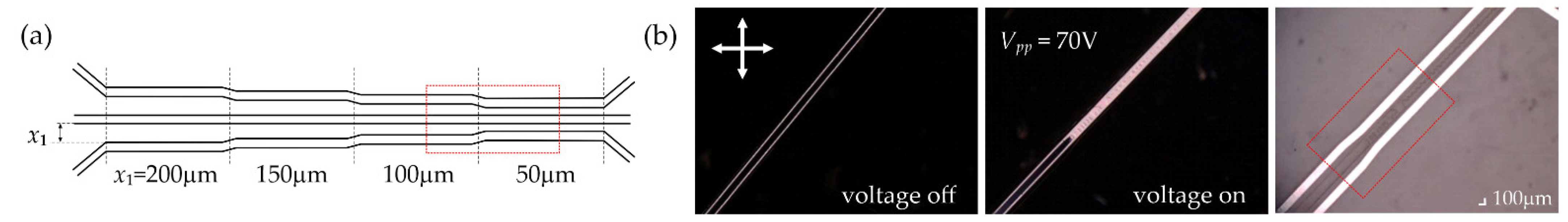
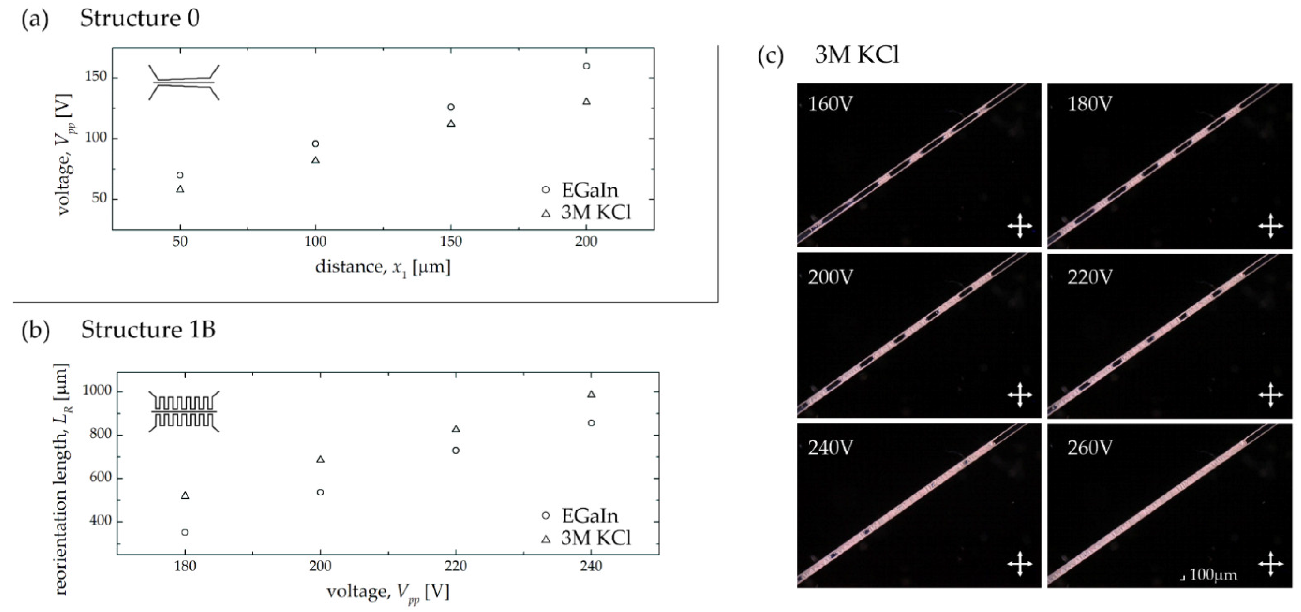
| Electrode Distance x1 [μm] | 50 | 100 | 150 | 200 |
| Peak-to-Peak Voltage Applied Vpp [V] | 70 | 96 | 126 | 160 |
| x1 [μm] | L1 [μm] | x2 [μm] | L2 [μm] | |
|---|---|---|---|---|
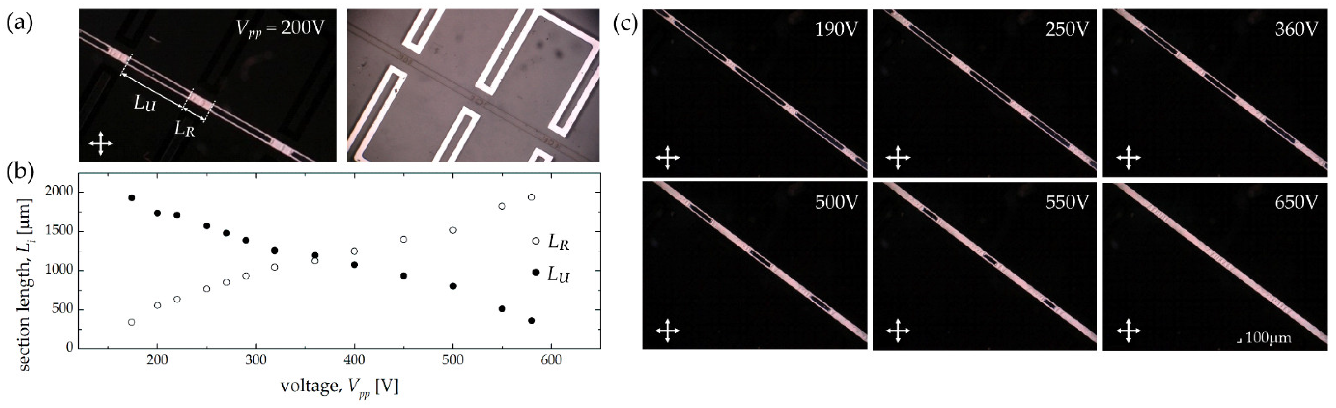
| Structure 1A | 200 | 575 | 2780 | 1725 |
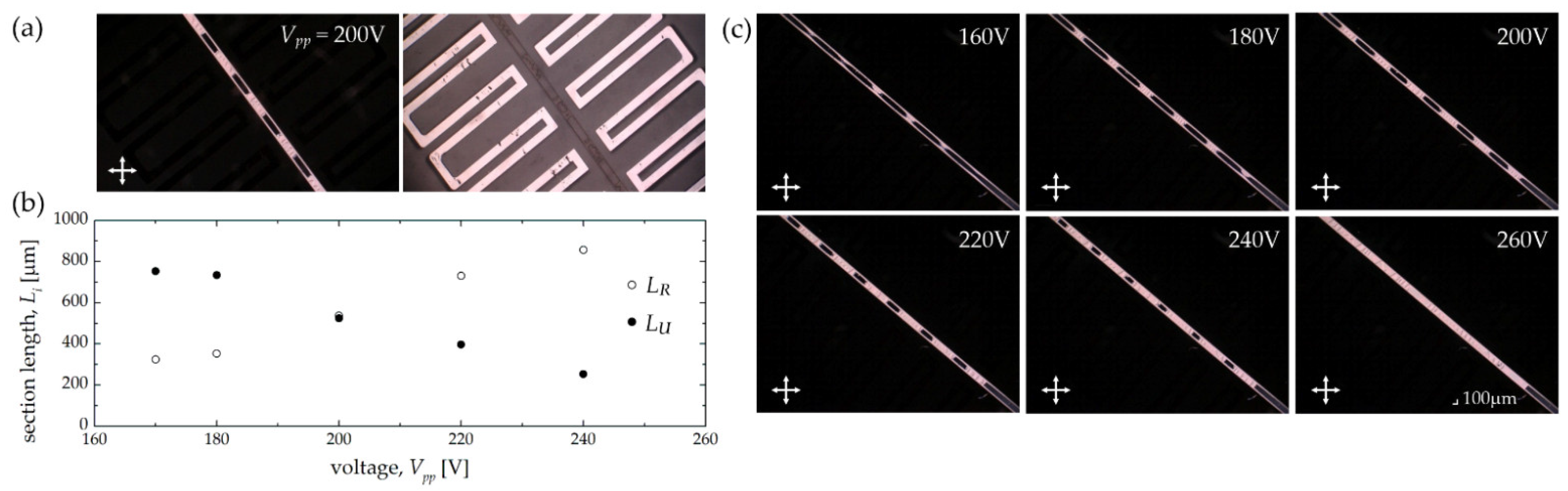
| Structure 1B | 200 | 575 | 2780 | 575 |
| x1 [μm] | L1 [μm] | x2 [μm] | L2 [μm] | |
|---|---|---|---|---|
| Structure 2A | 50 | 150 | 705 | 300 |
| Structure 2B | 50 | 300 | 695 | 150 |
Publisher’s Note: MDPI stays neutral with regard to jurisdictional claims in published maps and institutional affiliations. |
© 2022 by the authors. Licensee MDPI, Basel, Switzerland. This article is an open access article distributed under the terms and conditions of the Creative Commons Attribution (CC BY) license (https://creativecommons.org/licenses/by/4.0/).
Share and Cite
Rutkowska, K.A.; Sobotka, P.; Grom, M.; Baczyński, S.; Juchniewicz, M.; Marchlewicz, K.; Dybko, A. A Novel Approach for the Creation of Electrically Controlled LC:PDMS Microstructures. Sensors 2022, 22, 4037. https://doi.org/10.3390/s22114037
Rutkowska KA, Sobotka P, Grom M, Baczyński S, Juchniewicz M, Marchlewicz K, Dybko A. A Novel Approach for the Creation of Electrically Controlled LC:PDMS Microstructures. Sensors. 2022; 22(11):4037. https://doi.org/10.3390/s22114037
Chicago/Turabian StyleRutkowska, Katarzyna A., Piotr Sobotka, Monika Grom, Szymon Baczyński, Marcin Juchniewicz, Kasper Marchlewicz, and Artur Dybko. 2022. "A Novel Approach for the Creation of Electrically Controlled LC:PDMS Microstructures" Sensors 22, no. 11: 4037. https://doi.org/10.3390/s22114037