2.1. Planar Structures in Frequency-Variation Sensors
In this section, it is shown that sensitivity in frequency-variation microwave sensors implemented in planar technology can be optimized by adequately choosing the resonant element. Such a resonant element can be either a metallic resonator or a slot (also called defect-ground-structure DGS) resonator (a review of different electrically small resonant elements for sensing can be found in [
51]). Planar frequency-variation sensors can be implemented as transmission-mode or reflective-mode structures, but transmission-mode frequency-variation sensors are more common [
52]. Moreover, although transmission-mode frequency-variation sensors can operate either as notch filters or as bandpass filters, the former dominate the available literature. In this section, this study refers to sensors operating as transmission-mode notch filters, the notch being caused by the coupling (electric, magnetic or mixed) between the resonant element and the host transmission line. The consideration of a metallic or a slot resonator for sensor implementation may depend on several criteria. Nevertheless, slot resonators etched in the ground plane of a microstrip line exhibit an inherent advantage, i.e., such resonators are etched in the substrate side opposite to that of the line strip. Consequently, these sensors provide backside isolation, and the presence of the MUT is in contact, or in close proximity, to the sensing resonators does not alter the propagation along the line (except by the fact that the MUT modifies the resonance frequency of the sensing element). Thus, let us consider sensor implementation by means of slot-type resonators, such as the dumbbell defect-ground-structure (DB-DGS) resonator [
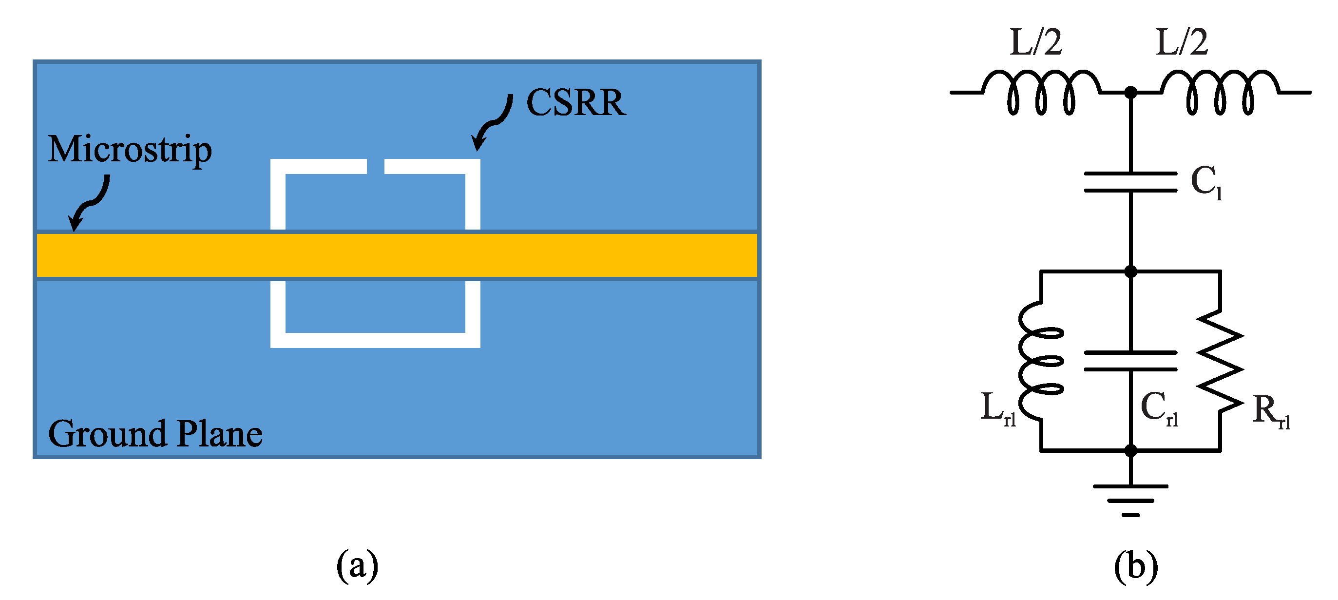
53], the complementary split-ring resonator (CSRR) [
54], and the open complementary split-ring resonator (OCSRR) [
55], to name a few.
Let us consider that the sensors under study are devoted to permittivity measurements. The canonical input and output variables are thus the dielectric constant of the material under study (or material under test
) and the resonance frequency, respectively. Nevertheless, if the imaginary part of the complex dielectric constant (or the loss tangent) should also be retrieved (second input variable), then an additional output variable is required. Such a variable is typically the magnitude of the notch (or peak, in case of bandpass-type sensing structures) [
18,
56,
57,
58]. The canonical sensitivity is thus defined as the derivative of the resonance frequency of the sensing element,
, with respect to the dielectric constant of the material under test (MUT),
, i.e.,
It is obvious that the variation in the resonance frequency generated by a change in the dielectric constant of the MUT should be larger in high-frequency sensors. Thus, for a faithful comparison between the sensitivities of different frequency-variation sensors, the relative frequency change is the one that should be considered. Therefore, the relative sensitivity, defined as
is the relevant parameter and figure of merit (useful for a realistic comparison) in these frequency-variation sensors. Assuming that the MUT is in the region of influence of the resonant element, a variation in the dielectric constant of the MUT alters the capacitance of such resonant element, and this in turn produces a shift in the resonance frequency. Thus, the relative sensitivity can be further developed and expressed as
where
is the capacitance of the resonant element loaded with the MUT. The first derivative in (
3) depends on the specific configuration of the line and sensing resonator, i.e., it depends on the analytical dependence of
with
. The second derivative in the relative sensitivity can be analytically obtained provided that several hypothesis and approximations are adopted [
52]. The first assumption considers the analysis restricted to fully planar resonant sensing elements etched in a single metallic layer and, therefore, exhibiting an edge capacitance. Namely, resonant elements implemented by means of two metallic layers, such as the broadside-coupled split-ring resonator (BC-SRR), or the microstrip step-impedance shut stub (SISS) resonator, both exhibiting a broadside capacitance, are excluded in the present analysis. It is also considered that the metal is an ideal (perfect) conductor, with negligible resistivity and thickness (this approximation is very reasonable in the usual metallization present in common microwave substrates, typically made of a high-conductivity material, such as Cu, and with thicknesses of the order of few tens of microns). The MUT is considered to be in contact with the resonant element, and occupying the whole half-space. That is, it is semi-infinite in the vertical direction (i.e., the direction orthogonal to the plane of the resonator), with transverse dimensions extending beyond the region occupied by the resonator. Moreover, the MUT is made of a uniform material. The substrate (also uniform) is sufficiently thick so that the effects of any potential metallic pattern in the face opposite to the one where the resonator is etched (e.g., the line strip) can be neglected (i.e., the resonance frequency is not altered by the presence of such patterns).
Let us consider a slot resonator etched in the ground plane of a microstrip line, and let us neglect the effects of the line on the capacitance (and resonance) of the resonator. If the substrate is thick enough to be considered semi-infinite in the vertical direction, it follows that the plane of the resonant element is a magnetic wall, and the electric field distribution at both half-spaces is a mirror image [
59]. Under these conditions, the electric field in the plane of the resonator is tangential, and the capacitance of the resonator can be separated in two parts, i.e., the capacitances associated with the lower and upper half-spaces (representing the contributions of the MUT and substrate, respectively), both connected in parallel. If we designate by C the capacitance of the bare resonator, i.e., without MUT (or surrounded by air), the capacitance
of the resonator loaded with an arbitrary MUT can be expressed as [
18,
52,
57,
58,
59]
where
is the dielectric constant of the substrate. According to (
4), the second derivative in (
3) is found to be
Concerning the first derivative in (
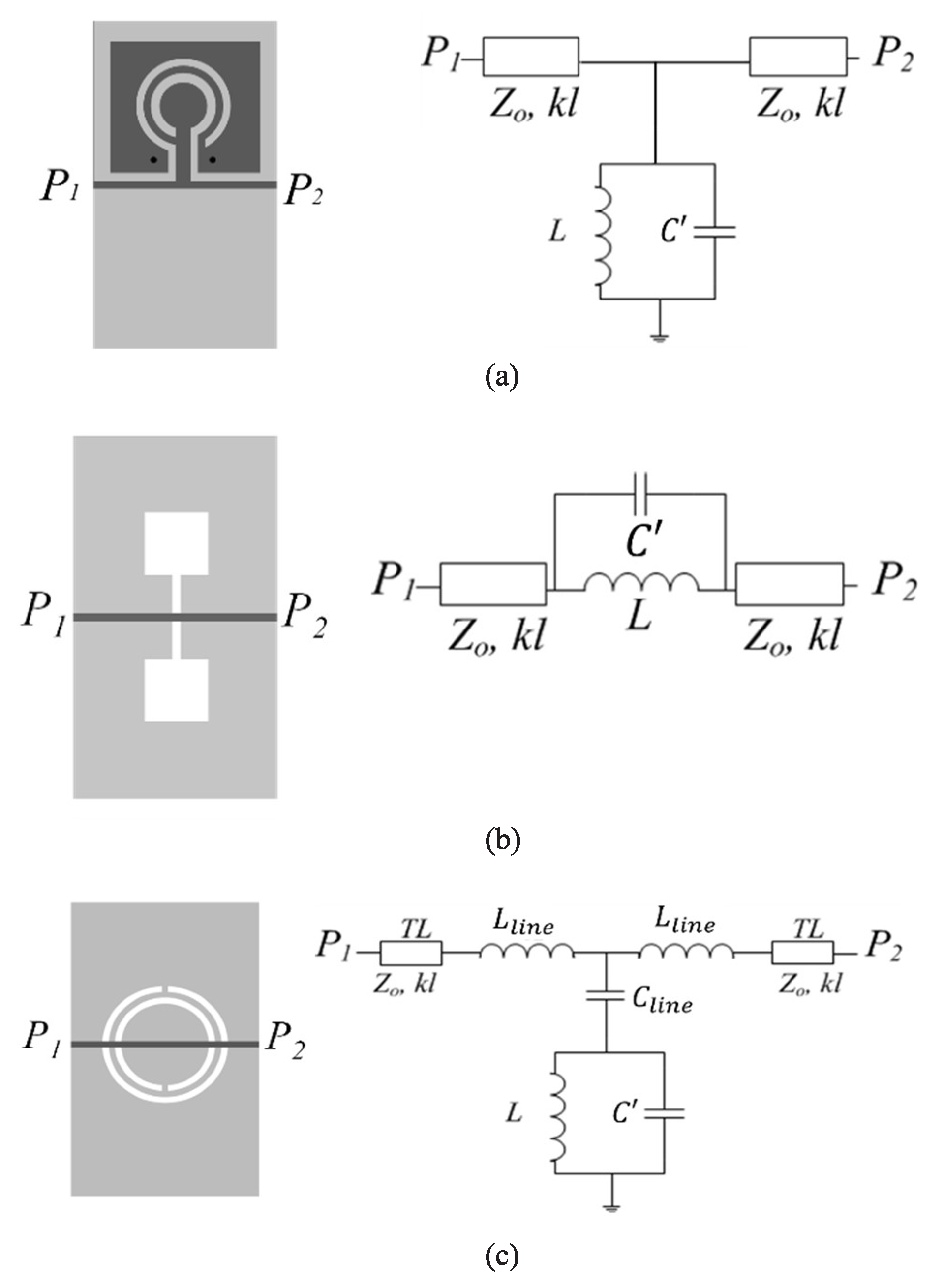
3), as indicated, it depends on the specific sensor configuration and resonant element. Let us consider three different resonant elements, the CSRR, the DB-DGS, and the OCSRR, loading a microstrip line, as depicted in
Figure 1. The circuit models of these structures are also depicted in Figure [
18,
39,
53,
60,
61]. It is clear that, for the OCSRR and DB-DGS resonators, the dependence of the resonance frequency on
is simply
whereas for the CSRR, the following result is obtained
where
L is the inductance of the resonator, not affected by the MUT, and
is the capacitance of the line section on top of the CSRR.
Using (
7), it follows that
and introducing (
8) and (
5) in (
3), the relative sensitivity for the CSRR-loaded line is found to be
It can be easily deduced that the relative sensitivity for the OCSRR- and the DB-DGS-loaded microstrip lines can be inferred from (
9) by simply forcing
= 0. From these results, it can be concluded that the relative sensitivity is superior in OCSRR- and DB-DGS-loaded microstrip lines, as compared to the CSRR-loaded lines. Moreover, from (
9 with
= 0), it follows that the relative sensitivity in sensors based on OCSRR and DB-DGS resonators does not depend on the geometry of the resonant element. However, note that the assumption of a semi-infinite MUT and substrate has been considered. Concerning the MUT, it is possible to machine it in order to be thick enough so that the semi-infinite approximation holds. In contrast, the substrate thickness is sometimes determined by external factors that do not depend on the designer, and, therefore, the semi-infinite substrate approximation cannot always be guaranteed. Despite that fact, even for relatively thin substrates, the plane of the resonant element is a quasi-magnetic wall [
59]. Under these circumstances, the capacitance of the resonator can still be considered to be formed by the parallel connection of the capacitance of the MUT and the capacitance of the substrate. Such capacitance is given by an expression formally identical to (
4), but replacing
with
, the latter being the equivalent dielectric constant of the substrate, defined as the dielectric constant of a hypothetical semi-infinite substrate providing the same contribution to the resonator’s capacitance [
59,
62]. This means that, for a finite substrate, the relative sensitivity for the CSRR-loaded line should be rewritten as
The equivalent dielectric constant depends on the ratio between the width of the capacitive slot and the thickness of the substrate [
59]. Consequently, for finite substrates, i.e., for substrates not satisfying the semi-infinite approximation, the relative sensitivity in OCSRR- or DB-DGS-loaded microstrip lines, given by (
10), does depend on the geometry. However, the dependence is soft, especially for relatively thick substrates, as it has been recently demonstrated [
59] (also note that, as the substrate thickness increases, the equivalent dielectric constant tends towards the nominal dielectric constant of the substrate, or
). Nevertheless, it can be concluded that regardless of the specific structure, for sensitivity optimization, it is convenient to deal with low dielectric constant substrates. In addition, it can be concluded from (
9) and (
10) that, as the dielectric constant of the MUT increases, the relative sensitivity decreases. Indeed, for high dielectric constant MUTs, the sensitivity scarcely depends on
(or
), since
obscures the substrate dielectric constant (or equivalent dielectric constant). In [
63], it was demonstrated that the relative sensitivity in an OCSRR- and DB-DGS-based sensor was very similar, and superior to the one obtained in a CSRR-based sensor (all implemented in the same substrate), in agreement with the theory. In this review paper, let us reproduce the results concerning the relative sensitivity achieved in various sensing structures based on a microstrip line loaded with a DB-DGS resonator (
is the strip width, whereas the DB-DGS is characterized by the width
S and length
l of the slot, and the width
and length
of the apertures, square-shaped in all cases), as can be seen in
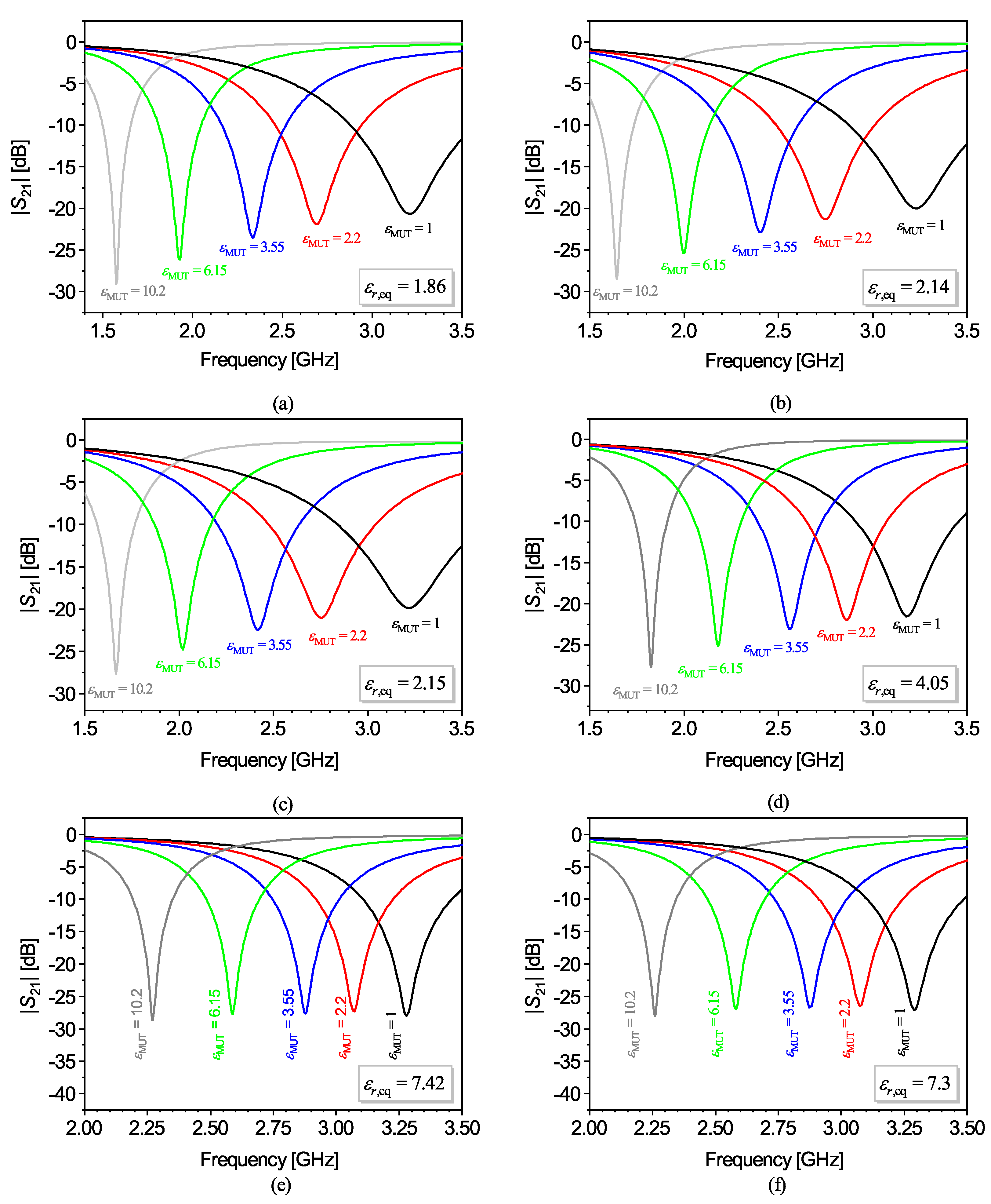
Table 1. The responses for MUTs with different dielectric constants (all semi-infinite in the vertical direction), inferred from electromagnetic simulation, are depicted in
Figure 2 [
59], where the equivalent dielectric constant is indicated.
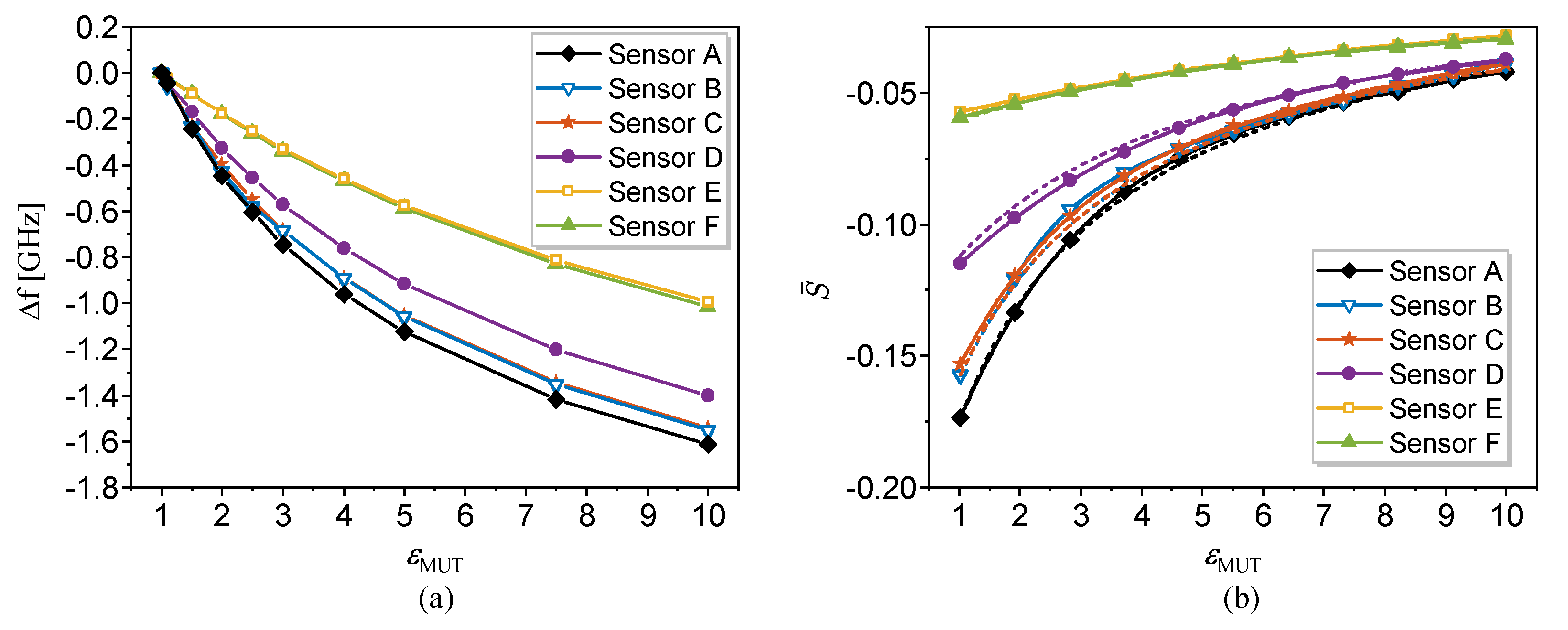
Figure 3a depicts the dependence of the resonance frequency with the dielectric constant of the MUT for the different sensors, whereas
Figure 3b depicts the relative sensitivity. The agreement between the relative sensitivity inferred from the derivative of the simulated data points and the analytical expression (
10) is excellent. Moreover, it can be appreciated from
Figure 2b that those sensors exhibiting the same (or roughly the same) equivalent dielectric constant exhibit an indistinguishable relative sensitivity, further pointing out the validity of the analysis.
In order to obtain the dielectric constant of an unknown material (MUT), isolating it from (
4) is the first step, which gives
Note that, in (
11), we replaced the dielectric constant of the substrate by the equivalent dielectric constant in order to take into account the finite thickness of the substrate. If the considered resonator is the DB-DGS (or the OCSRR), with the resonance frequency given by (
6), then (
11) can be rewritten in terms of the resonance frequency of the bare resonator,
, and in terms of the resonance frequency of the resonator loaded with the MUY,
, i.e.,
For CSRR-based sensors, the ratio
that appears in (
11) can be evaluated by isolating
C and
from (
7), however, the resulting expression is not as simple as (
12). In this case, it is found that
is
and the dielectric constant of the MUT is inferred by introducing (
13) in (
11). Another important aspect is the determination of the equivalent dielectric constant of the substrate. For this purpose, the idea is to use (
12), for DB-DGS (or OCSRR) based sensors, and consider a MUT with well-known dielectric constant. By measuring, or simulating, the response of the bare sensor, and the one of the sensor loaded with that MUT,
, can be isolated from (
12). If, in contrast, a CSRR is the sensing element, in this case, (
13) and (
11) must be used. The experimental validation of frequency-variation permittivity sensors based on different resonant elements, such as CSRRs, SRRs or DB-DGS resonators, has been reported in the literature [
18,
58].
Table 2 depicts a comparison of various frequency-variation sensors. In the table,
is the frequency of the bare resonator.
is the average sensitivity, calculated as the ratio between the output dynamic range (or difference between the resonance frequency of the bare resonator and the resonance frequency of the resonator loaded with the MUT exhibiting the maximum dielectric constant) and the input dynamic range (difference between the maximum and minimum values of
). Finally,
is the relative average sensitivity, calculated by simply dividing the average sensitivity by the resonance frequency of the bare resonator, i.e.,
) (nevertheless, note that in the table,
is expressed as a percentage). The table includes also the considered input dynamic range relative to the dielectric constant of the MUT.
According to the results of
Table 2, the sensor reported in [
58] exhibits by far the higher relative average sensitivity. It should be mentioned that the substrate dielectric constant in the sensors of [
64,
66] is
, and this explains, in part, the limited relative average sensitivity in such sensors. However, in the sensors reported in [
28,
65], the dielectric constant of the substrate is
and
, i.e., smaller than the substrate dielectric constant considered in the sensor of [
58] (
). The reason that explains the superior relative average sensitivity in the sensor of [
58] is the considered resonator, a DB-DGS. With such a sensing resonant element, the changes in the dielectric constant of the MUT directly affect the unique capacitance that determines the resonance frequency, the output variable (see expression (
6)). In contrast, in the sensors presented in [
28,
65], where a complementary split-ring resonator (CSRR) was used, the resonance frequency is also dependent on the coupling capacitance between the line and the resonant element (
), as can be seen in the expression (
7). Since such capacitance does not vary with the dielectric constant of the MUT, it is expected that such CSRR-based sensors exhibit poorer sensitivity, as compared to those of DB-DGS-based sensors.
2.2. Exploiting the Coupling between Resonators
Recently, it was shown that the sensitivity of CSRR-based sensors can be considerably enhanced by loading multiple CSRRs to a microstrip line (or antenna) and exploiting the inter-resonator coupling between them [
33,
34,
67]. In [
33], it was theoretically and experimentally demonstrated that when the resonators are placed such that their coupling takes place in the plane transverse to the direction of propagation (along with the microstrip line), the sensitivity of the sensor enhances. It was also shown that increasing the number of resonators creates more sensitive modes (transmission zeros). In [
34,
67], highly sensitive sensors based on coupled CSRRs were applied for sensing glucose levels in the blood and aqueous solutions.
Let us first study how the mutual coupling between resonators can enhance the sensitivity of a CSRR-based sensor [
33].
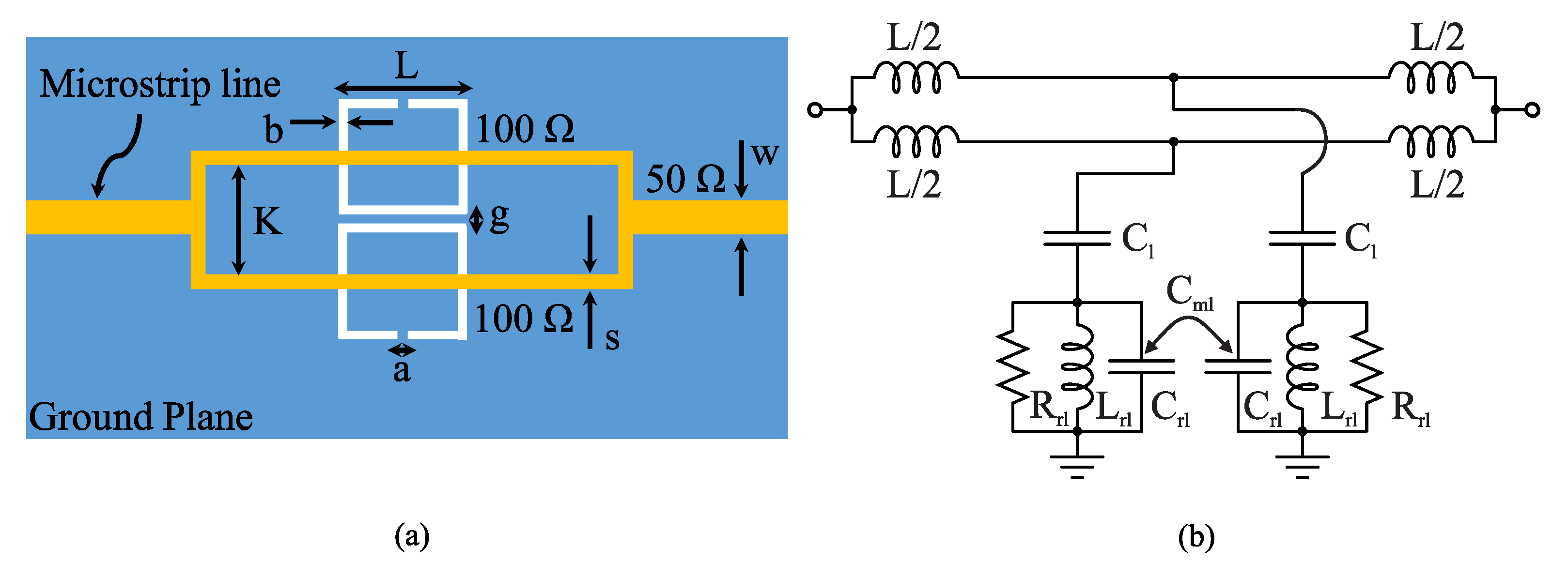
Figure 4a shows a microstrip line loaded with a single CSRR. The CSRR can be considered as a quasi-static resonator and modeled using an RLC circuit as shown in
Figure 4b. In this figure,
and
L are the per unit-length capacitance and inductance of the transmission line and
and
are the effective capacitance and inductance of the resonator. The circuit shown in
Figure 4b exhibits a transmission of zero at its resonance frequency given by
Loading the CSRR with a dielectric material increases the resonator’s capacitance (
) due to the higher unity of the sample’s relative permittivity, which decreases the resonance frequency. In
Figure 5a, loading a microstrip line with two CSRRs is considered. For stronger coupling between the line and CSRRs, the resonators are individually excited using two branches of the transmission line in the form of a splitter–combiner microstrip Section [
68].
Figure 5b shows the lumped circuit model for the splitter–combiner microstrip section loaded with two CSRRs [
68]. In this figure,
is the mutual capacitance modeling the inter-resonator coupling between two CSRRs. Notice that since the resonators are electrically very close to each other, the inter-resonator coupling is appreciable. Considering that the coupling between the two transmission line sections is very low, the resonance frequency (in which a transmission zero occurs) can be approximated by [
68],
where
is the resonance frequency without the inter-resonator coupling between the CSRRs given in (
14). From (
15), the inter-resonator coupling (
) causes an increase in the resonance frequency.
To analyze the sensitivity of the 1CSRR sensor compared to that of the 2CSRR sensor, the assumption of a small change in the resonance frequency due to the perturbation caused by the MUT was made. Since the MUT mostly affects the resonator capacitance (
), the derivative of the resonance frequency with respect to
can be considered as a measure of the sensitivity. For the 1CSRR sensor, in (
14), we have
whereas for the 2CSRR sensor, in (
14), we have
It can be seen that compared to the changes in the resonance frequency of the 1CSRR sensor (i.e., (
16)), the inter-resonator coupling capacitance (
) in (
17) makes the resonance frequency of the 2CSRR sensor more sensitive to the change in the resonator capacitance (
); hence, a higher sensitivity to the change in the MUT can be achieved.
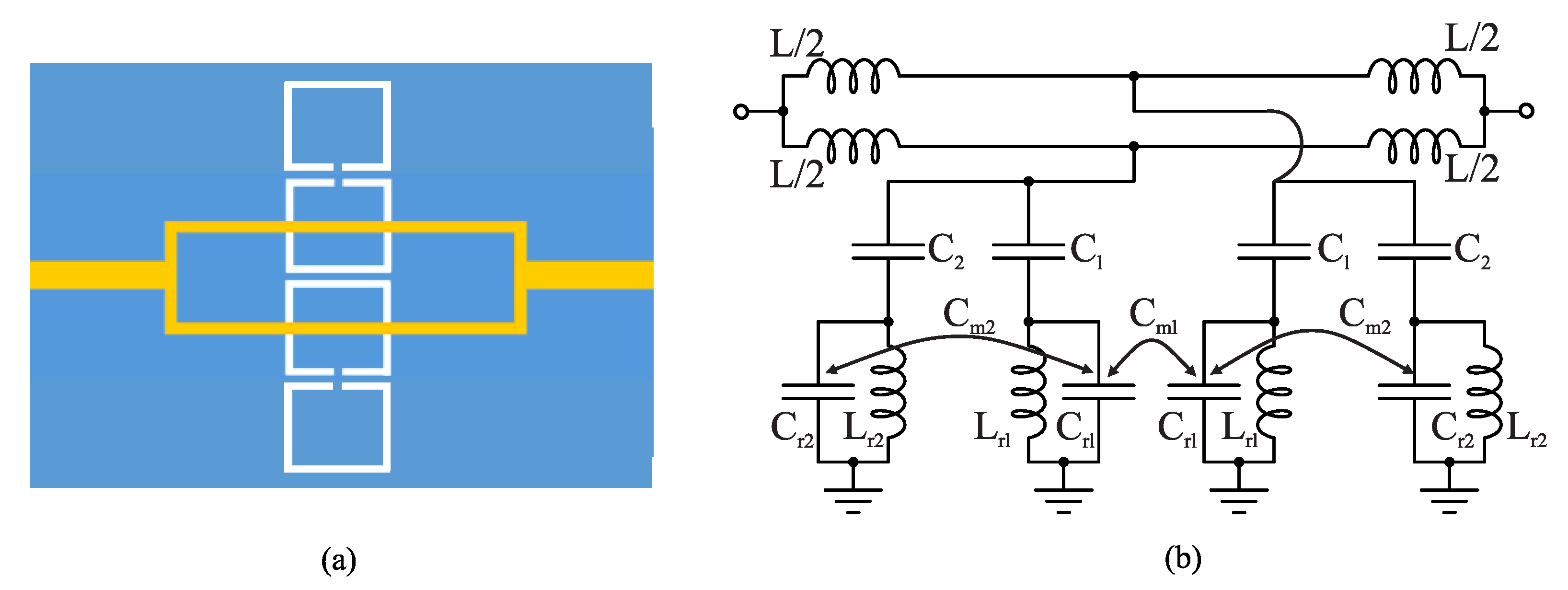
To further increase the sensitivity, four resonators can be coupled to two transmission lines as shown in
Figure 6a.
Figure 6b shows the lumped circuit model in the case of the four resonators. Since the two feeding transmission lines are not in the center islands of the two additional resonators, it is expected that their coupling capacitance (
) becomes weaker. The new mutual coupling can be represented as an inter-resonator capacitance (
). In addition, since we have two sets of coupling capacitances (
and
) as well as two inter-resonator mutual coupling capacitances (
and
), it is expected that the sensor exhibits a dual-band rejection (i.e., two transmission zeros).
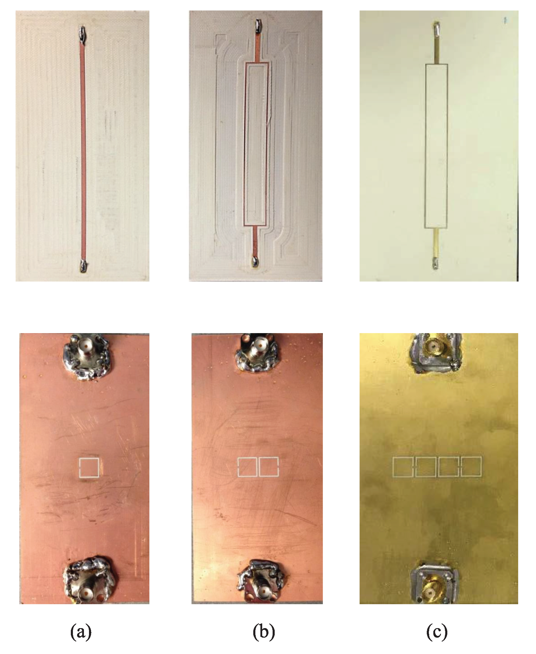
As a proof of concept, the authors of [
33] designed a 50
microstrip line loaded with a CSRR on a Rogers RO4350 laminate with a thickness of 0.75 mm such that the resonance frequency (transmission zero) occurs at approximately
. They also designed the 2CSRR and 4CSRR sensors so that each CSRR’s dimensions are the same as that in the 1CSRR sensor. The sensors were fabricated as shown in
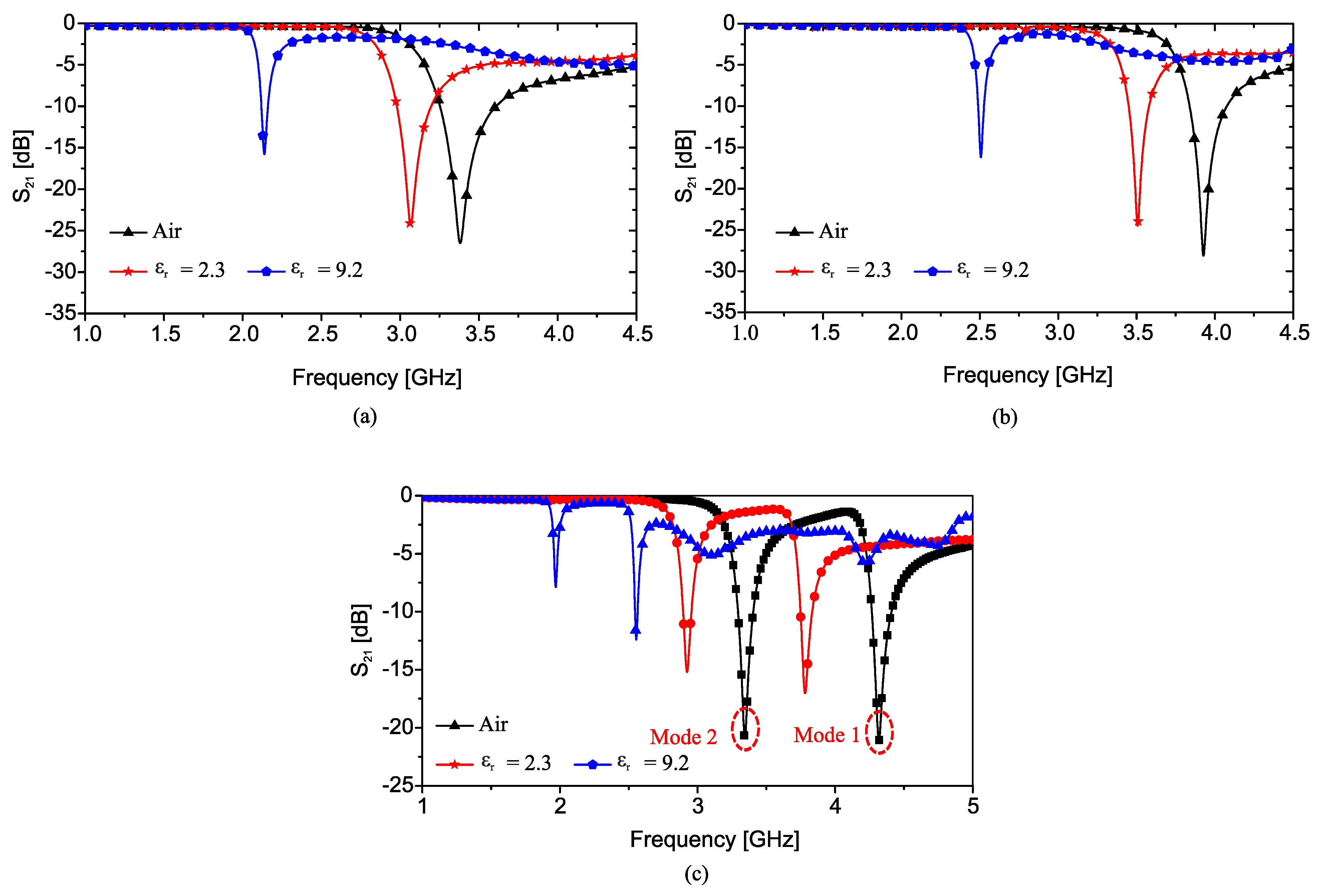
Figure 7. The measured transmission coefficient (|
S) parameters of the sensors when unloaded as well as when loaded with Rogers RT/duroid 5870 and TMM10 laminates having dielectric constants of 2.3 and 9.2 are shown in
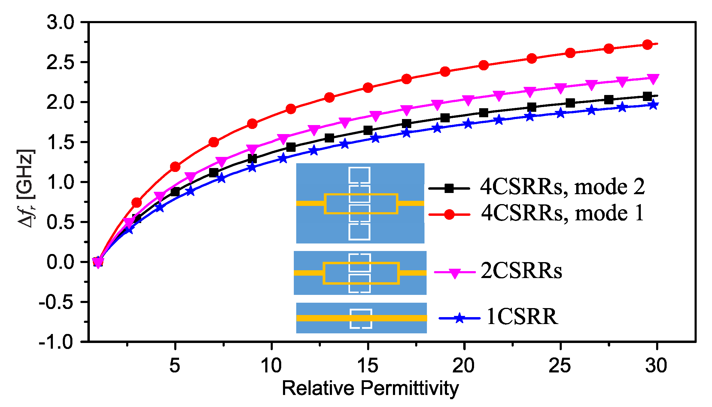
Figure 8. As seen in this figure, the resonance frequency of the unloaded 2CSRR sensor is approximately 3.9 GHz, i.e., approximately 500 MHz higher than the resonance frequency of the 1CSRR sensor, which agrees with the analysis of the equivalent circuit models. The 4CSRR sensor, as expected from its equivalent circuit model, also shows two transmission zeros (resonances) at approximately 4.3 GHz (first mode) and 3.4 GHz (second mode). Compared to the reference case (unloaded sensors), the shifts in the resonance frequency when loaded with RT/duroid 5870 and TMM10 laminates are 313 MHz and 1243 MHz for the 1CSRR sensor, 420 MHz and 1420 MHz for the 2CSRR sensor, and 515 MHz and 1742 GHz for the first mode of the 4CSRR sensor. Moreover, for a better comparison between the sensitivity of three sensors, in the full-wave simulations, the dielectric constant of an MUT (filling the CSRRs’ area) was varied from 1 to 30.
Figure 9 shows the shifts in the resonance frequencies of the 1CSRR, the 2CSRR and the 4CSRR sensors.
Figure 8 and
Figure 9 demonstrate that, as expected from the analysis of the equivalent lumped circuits, the 2CSRR sensor shows appreciably higher sensitivity than the 1CSRR sensor. In addition, in the case of the 4CSRR sensor, mode 1 shows much higher sensitivity to changes in the dielectric constant of the MUT. This validates the concept of exploiting the coupling between resonators to enhance sensitivity.
In [
34], as shown in
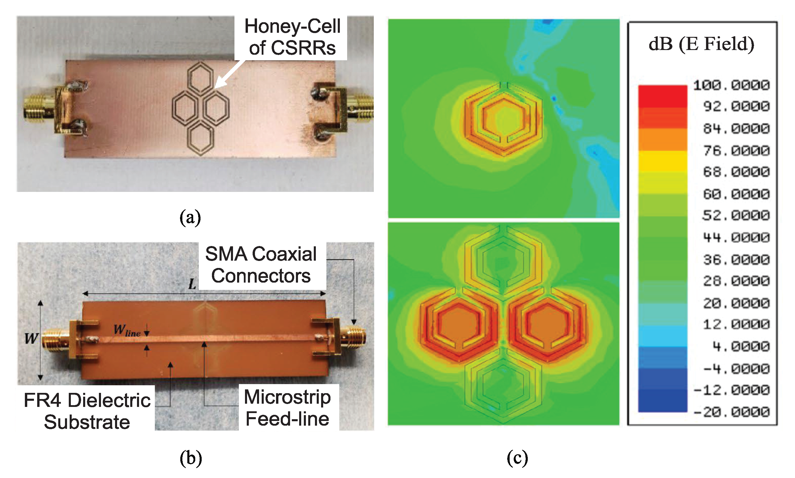
Figure 10a,b, four hexagonal-shaped CSRRs, arranged in a honey-cell configuration and coupled to a microstrip line, were applied for monitoring the blood glucose level. Due to the resonant feature of the CSRRs, transmission zeros appear at the
of the line.
Figure 10c indicates a comparison between the electric field distributions (at a 3 GHz resonant frequency) on the ground plane when a honey-cell (including four coupled hexagonal CSRRs) and a single hexagonal-shaped CSRR are etched on the ground plane. It can be seen that the honey-cell design exhibits higher electric field localization with an intensity up to
over the CSRR area compared to that of a single hexagonal cell. Due to the high intensity of the electric field coupled to the honey-cell area (around the dielectric slits and the routes in-between), this area is identified as the sensing region for the glucose samples to acquire strong interaction with the coupled near-field and therefore induce notable variations in the intrinsic characteristics of the sensor in response to subtle variations in the EM properties of different glucose concentrations.
Two preliminary honey-cell prototypes (compact and dispersed) were numerically modelled, fabricated and experimented with for monitoring the glucose level.
Figure 11 shows the experimental setup using a vector network analyzer (VNA). For the sake of simplicity, aquatic glucose solutions were used in these experiments to imitate the blood behaviour at different glucose concentrations (70–120 mg/dL) clinically relevant to type-2 diabetes. This approximation is valid since water contributes approximately
of the entire human blood that contains other vital components at varying proportions. These minerals are present at lower concentrations compared to the dominant glucose, whereby the blood dielectric properties are dominantly affected. A cylindrical glass container was fabricated to hold the samples on top of the CSRR surface (see
Figure 11). The empty cylindrical container was placed on the honey-cell CSRR structure, as shown in
Figure 4b. This will introduce a few MHz shifts from the reference resonance in
S21 of the unloaded state. In each measurement trial, a micropipette device was used to measure a precise volume of
L from each concentration, load it inside the container, and the change in the transmission resonance frequency response was recorded.
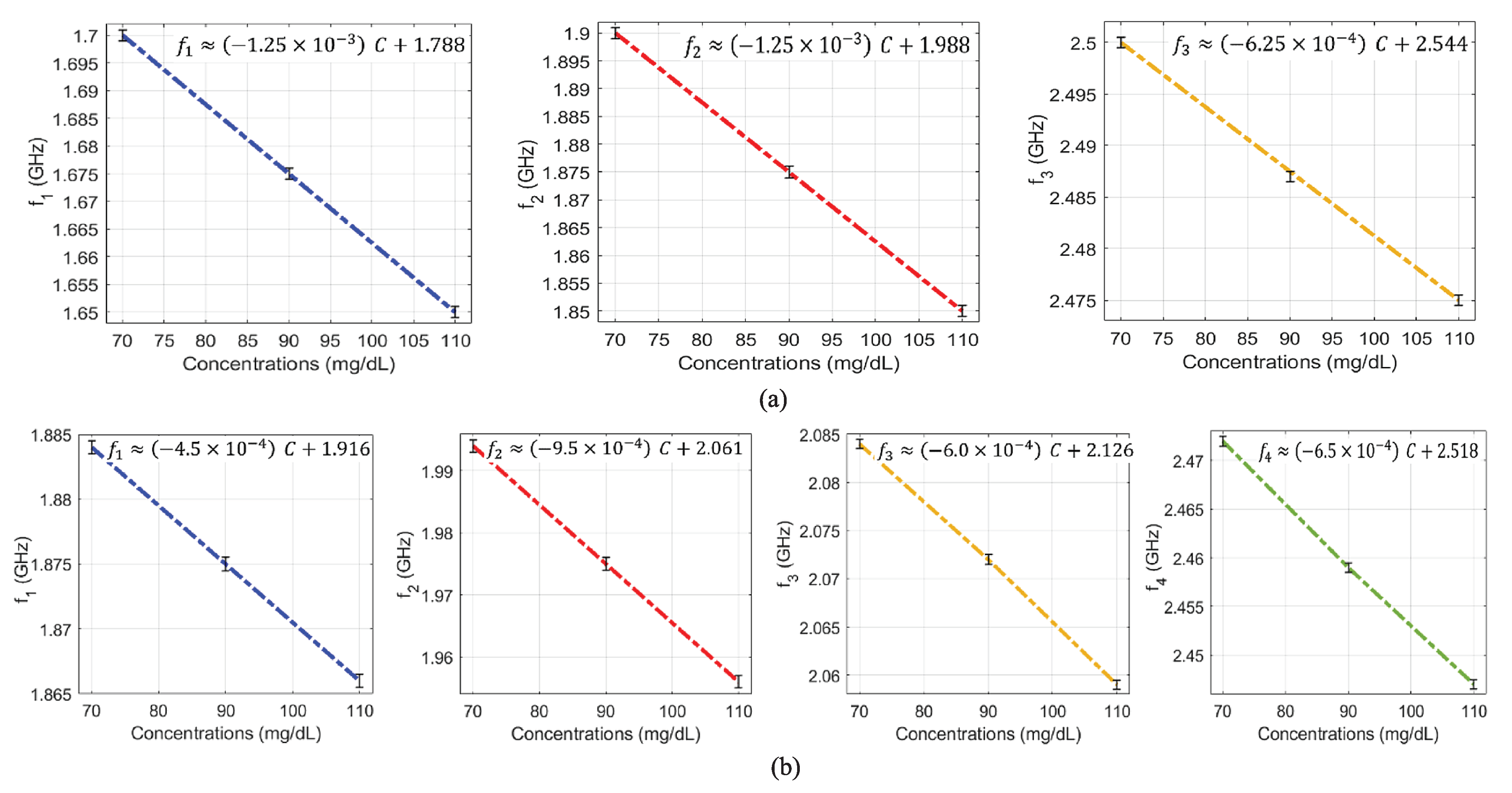
Figure 12a,b, respectively, show the transmission responses of the compact and dispersed sensors when the concentration of glucose is changing in 70, 90 and 110 mg/dL. In the compact prototype, as shown in the inset of
Figure 12a, the CSRRs are located close together; hence, there is a strong mutual coupling between them. Whereas in the dispersed prototype indicated in the inset of
Figure 12b, the CSRRs are spaced apart, and the mutual coupling is weak. In these figures, three and four transmission zeros are observed in the response of the compact and dispersed sensors, respectively. In both sensors’ responses, it is observed that the resonant frequencies at which the transmission is minimized are shifted towards lower frequencies as the glucose concentration in the sample increases. Linear correlation models for the resultant resonant frequencies of compact and dispersed sensors at different glucose concentrations were derived, which are shown in
Figure 13a,b, respectively (conversely, the inverse models could be used to estimate the unknown glucose level of a tested sample). It is observed that the respective resonant frequencies decrease with increasing levels of glucose concentrations. However, the frequency resolutions for glucose level changes at the respective resonances are not identical. The sensitivity of the compact sensor is estimated as −1.25/(mg/dL), representing the gradient of
and
linear models. However, the best sensitivity slope for the dispersed topology (where the mutual coupling between the resonators is weak) is recorded as −0.95/(mg/dL) at
, which is lower than the compact counterpart having a strong coupling between its CSRRs. This demonstrates the positive impact of mutual coupling on sensitivity.
In another similar recent work [
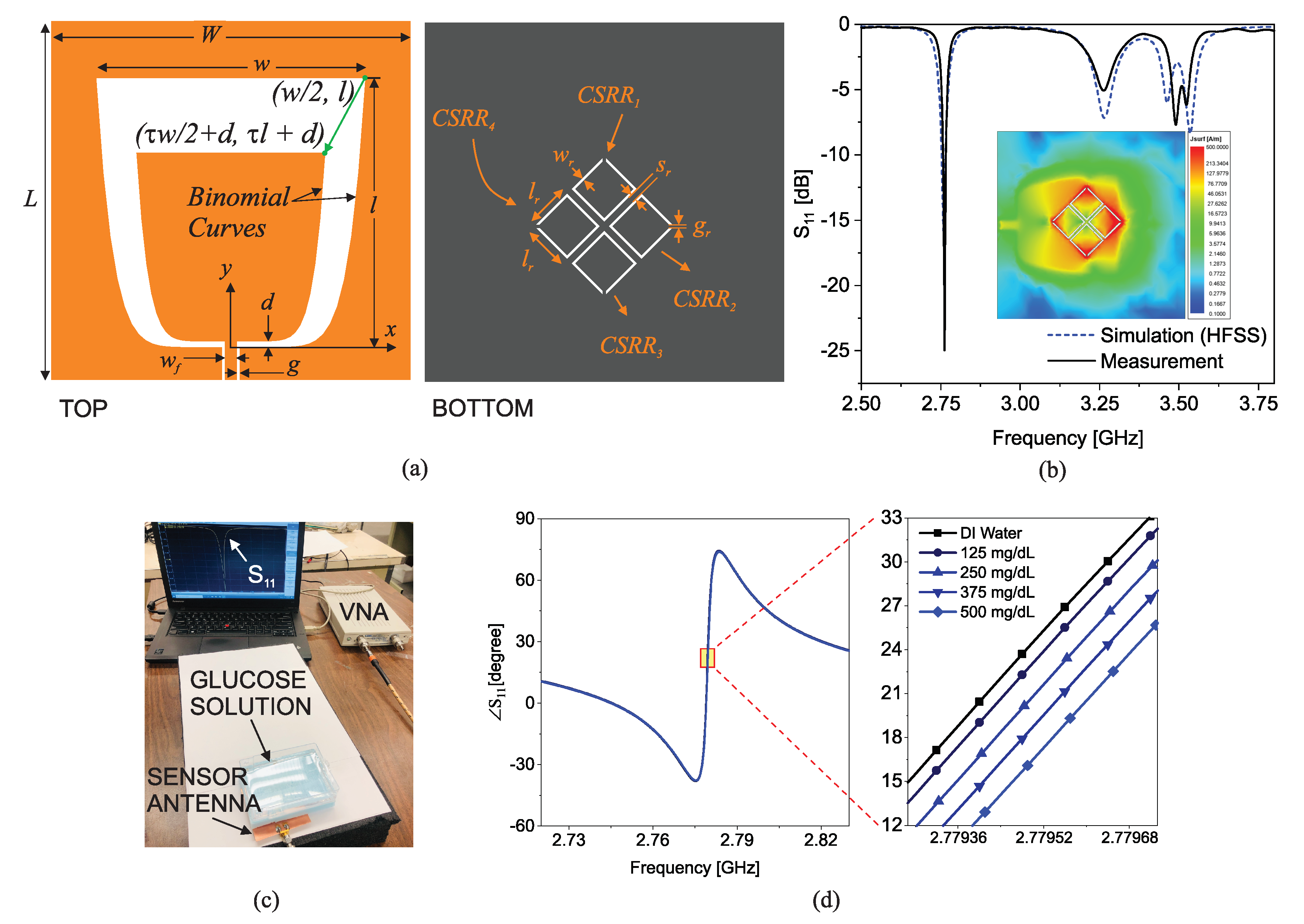
67], a planar sensor antenna consisting of coupled CSRRs excited by a binomial slot antenna was introduced for glucose sensing. A schematic of the proposed sensor antenna is shown in
Figure 14a. A wide-band CPW-fed printed slot antenna with a binomial curve, as shown on the left side of the figure, is designed on the top of a dielectric substrate to have a good matching within 2.6–3.6 GHz bandwidth. On the bottom of the substrate, as shown on the right side of
Figure 14a, four identical CSRRs are etched.
The measured and simulated responses (
) of the sensor antenna are shown in
Figure 14b indicating a good agreement between them. A deep resonance is observed at 2.78 GHz which is not produced by only one CSRR but is uniquely formed by the mutual interaction of four of them as can be verified by the surface current density given in the inset over all resonators. In fact, the objective of this work was to enhance the sensitivity by exploiting the mutual coupling between the four resonators. The phase-response of the sensor at the lowest resonance frequency (i.e., 2.78 GHz) was used to sense the glucose level in aqueous solutions due to its high sensitivity. Notably, the dielectric constant of the aqueous solution decreases at a higher glucose content, thereby increasing the resonance frequency. This upshift leads to a drop in the phase when monitored at a single frequency. As a proof of concept, four samples of aqueous solution with 125 mg/dL increments were prepared. As shown in
Figure 14c, the samples were held 5 mm above the sensor (using foam) within a plastic container to emulate the thickness of skin, fat and muscle layers. The phase response of the sensor was measured, as shown in
Figure 14d. This figure shows that the phase at 2.78 GHz changes from 25.4 to 17.2 degrees for a glucose level change of 0–500 mg/dL, with a sensitivity beyond 0.5 degrees corresponding to 30 mg/dL.
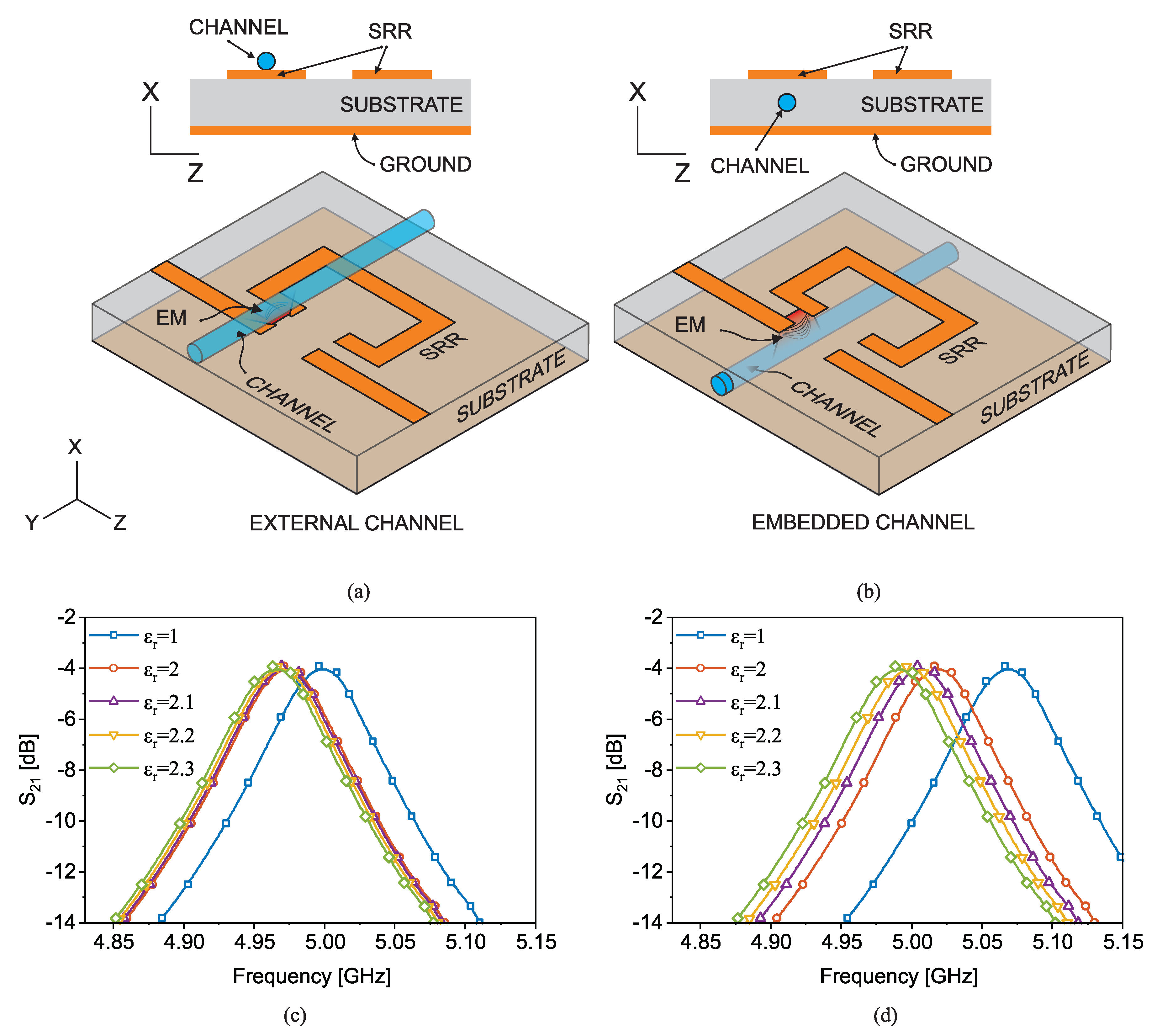
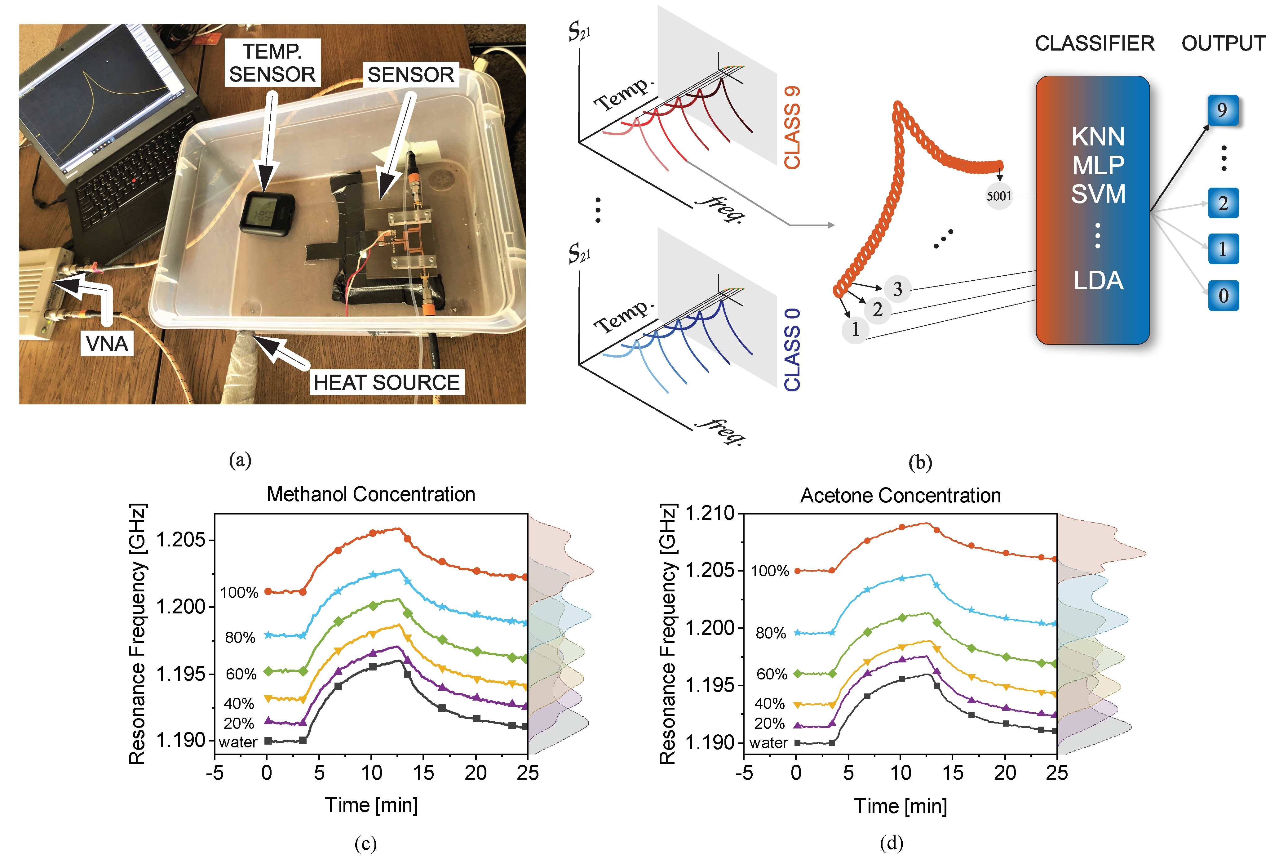
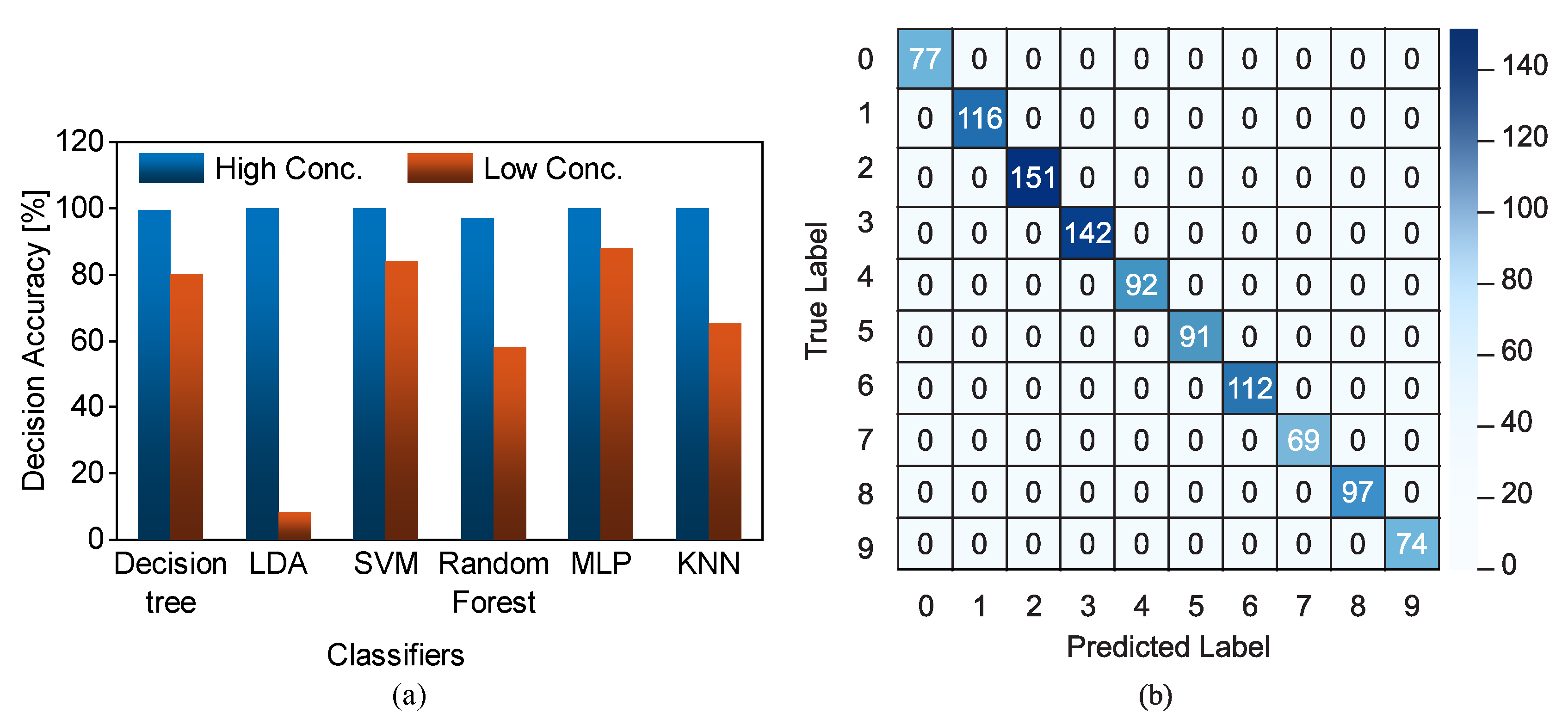
2.3. Embedded Channels in the Substrate
In this section, the substrate of a microwave sensor is shown that can be exploited as the analyte carrier to boost the sensor sensitivity. Microwave sensors are typically designed on low-permittivity substrates as the base of the sensor. This low-permittivity is essentially because of the overall interaction of a substrate with the sensitivity. To elaborate on this, let us consider a planar half-wavelength (
) resonator (open to free space) that is supported by a dielectric substrate backed by a ground plane as shown in
Figure 15. The sensor’s resonance frequency is governed by:
where
and
denotes the effective inductance and capacitance seen by the resonator including the substrate and background materials in the proximity of the resonator (
). Then, any change in a dielectric material under test results in capacitance variation is as follows:
where
is the capacitance of a bare resonator without the presence of any external interfering material, and
represents the whole impact of an external analyte. This expression suggests that the resonance frequency shifts according to a percentage change in the overall capacitance of a resonator. Therefore, a high sensitivity can be achieved by increasing the ratio of
. As a result, the substrate that is a contributing factor for
needs to be chosen to be low as not to obscure the material’s impact. In this regard, since typically
, one can exploit the very main contributing factor rising from the substrate. In such a case as that shown in detail in [
36], the substrate can be used as the carrier of the material as opposed to a case where the MUT is separate from the substrate with a minimal impact on modifying the total capacitance
. By properly embedding the material inside the substrate,
changes significantly since the majority of electric fields between the resonator and the ground plane become disturbed. According to the diagram shown in
Figure 15a, conventional placement of the channel is outside the resonator flushed with the sensor surface when exposing the material to the sensor with shortest possible distance. The electric fields interacting with the MUT are emanating fields fringing from the transmission line into air and terminating at the resonator. In contrast, the method studied in [
36] is represented in
Figure 15b in detail where the microfluidic channel is embedded within the substrate. This configuration allows for higher interaction between MUT and the resonator-to-ground electromagnetic fields, which leads to higher sensitivity.
Two sensors with 1.2 mm-thick SRRs with ≈22 mm length and a 3 mm gap that is separated from the adjacent transmission line by 0.4 mm are simulated in a full-wave high-frequency simulator (HFSS) [
36]. In this simulation, a cylindrical hole inside the substrate is filled with various lossless dielectric materials with
. The bare sensor resonates around
when the substrate is chosen to be 0.79 mm-thick Rogers RO5880 with dielectric properties of
and
. The transmission response of the sensors (
) is recorded with respect to the variations in the material property, as shown in
Figure 15c,d. In the case of external tubing, the tube is flushed on the resonator as shown in
Figure 15a (top) and in the embedded channel, a hollow cylinder is emptied out of the substrate and replaced with the tube as shown in
Figure 15b (top). The orientation of the tube is under the edge of the SRR as well as the feeding transmission line to improve the sensitivity. Simulation results reveal that the frequency shift in the transmission profile of the sensor with the external channel negligibly changes when the filling material permittivity varies. However, this resonance frequency shift is largely increased in the case of an embedded channel. It can be observed that the resonance frequency shift of the sensor with the external channel is ≈170 MHz/
while the embedded channel leads to the much higher sensitivity of ≈440 MHz/
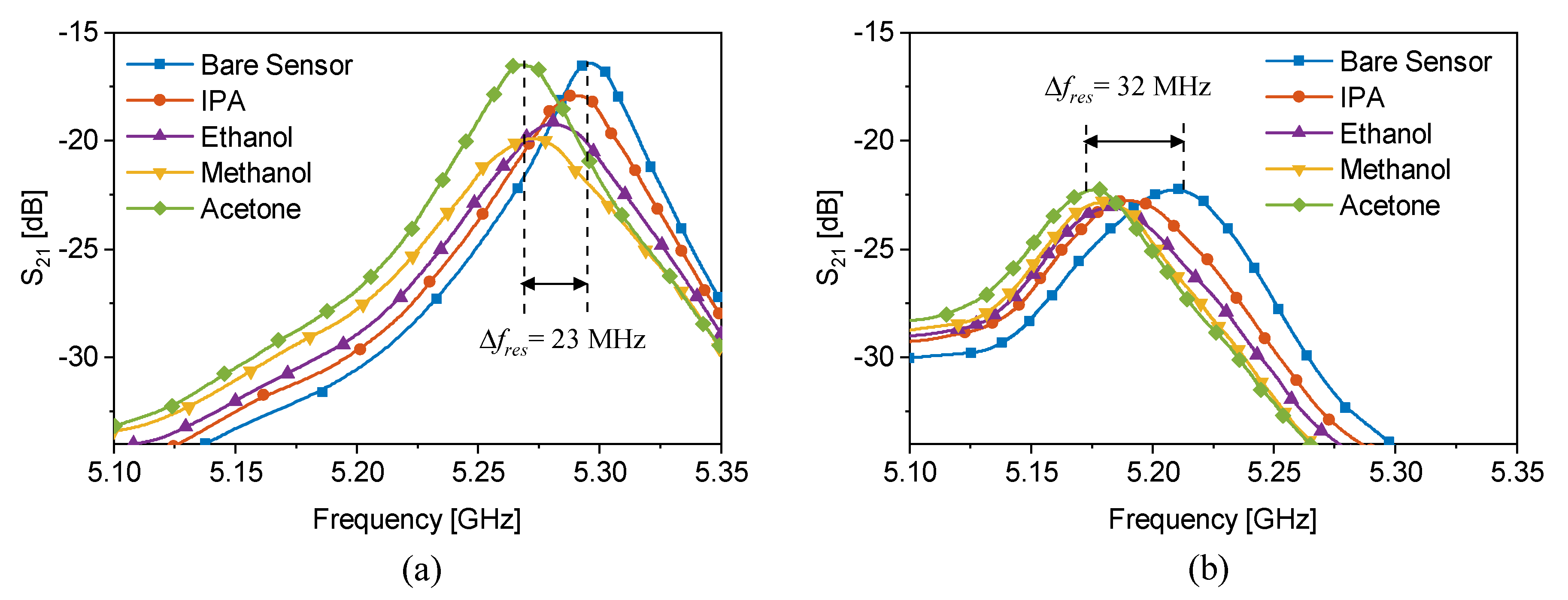
for permittivity variations between 2 and 2.3, leading to an improvement of 250%. The experimental verification of such sensors is also elaborated by measuring common chemicals including IPA (
,
), ethanol (
,
), methanol (
,
) and acetone (
,
). The polytetrafluoroethylene (PTFE) microfluidic tube used in this experiment is with inner/outer diameter of 0.8/1.6 mm, respectively, and 0.4 mm wall thickness. The measured transmission profiles with liquid analytes are shown in
Figure 16a,b. Since the comparison is between sensors with the similar bare resonance frequencies, the sensitivity S in this case is defined as
as computed in detail in
Table 3. Frequency shifts in material characterization are engineered to exhibit improvements up to 259% (e.g., IPA) with a change in the sensing configuration, while the sensor architecture as well as the initial operating frequency remain unchanged.
2.5. Resonator Pattern Optimization
Nowadays, using computer-aided design (CAD), microwave designers are capable of delivering designs that meet the predefined requirements as long as these requirements are not extreme. For this purpose, they first draw a topology of the design according to the classical methods, and then using optimization techniques, which are embedded in almost all CAD packages, they optimize the sizes, dimensions and other parameters to achieve the required goals. The question which may arise is that of where “it is the best design one can achieve”. Since the optimization is about changing the dimension of the model, not its shape and topology, the performance of the final optimized design highly depends on the initial design topology and so it may not be the best solution. What if there is a way to find the optimum design without having an initial model? If that were the case, the design can be performed in a fully automated, complete-cycle procedure.
Robust methods have been introduced to fully automate and optimize the design of microwave planar devices (fabricated with printed circuit board technology), such as radar cross-section reducer surfaces [
73,
74,
75], high impedance surfaces [
76,
77], electromagnetic energy harvesting surfaces [
78], absorbers [
79], decoupling elements between microstrip antennas [
80], polarization converters [
81,
82], and frequency-selective surfaces [
83]. In this method, the shape of the artworks (the pattern to be etched into each copper layer of a PCB) is optimized to achieve the best possible performance. This optimization is not about changing the dimensions of a model but rather about its shape. The required optimization procedure is essentially making a decision as to which parts of the pattering area are covered with metal and which parts are not (etched). In particular, this versatile design approach was also applied to the design of high-sensitivity planar sensors [
37,
84,
85]. In microwave sensors based on electrically small planar resonators (ESPRs), the shape of the resonator plays an essential role in the sensitivity. Due to the high-field localization on the ESPR area, in such sensors, the MUT is placed on the resonator area, where there is a strong interaction between the highly localized field with the MUT, which leads to a change in the sensor’s response. The resonator’s shape can affect the field distribution and localization in the sensitive area, and thus the sensitivity. Therefore, the shape of the resonator can be optimized to achieve the highest possible sensitivity.
In [
37], a highly sensitive CSRR-based sensor was developed in a complete-cycle topology optimization procedure for the highly accurate characterization of dielectric materials. In this design approach, the sensing area (the CSRR area) was first pixelated. Then, by maximizing the sensitivity as a goal, a binary optimization algorithm was applied to determine whether each pixel was metalized. The outcome of the optimization is a pixelated pattern of the resonator yielding the maximum possible sensitivity. Some details of [
37] are provided in the following.
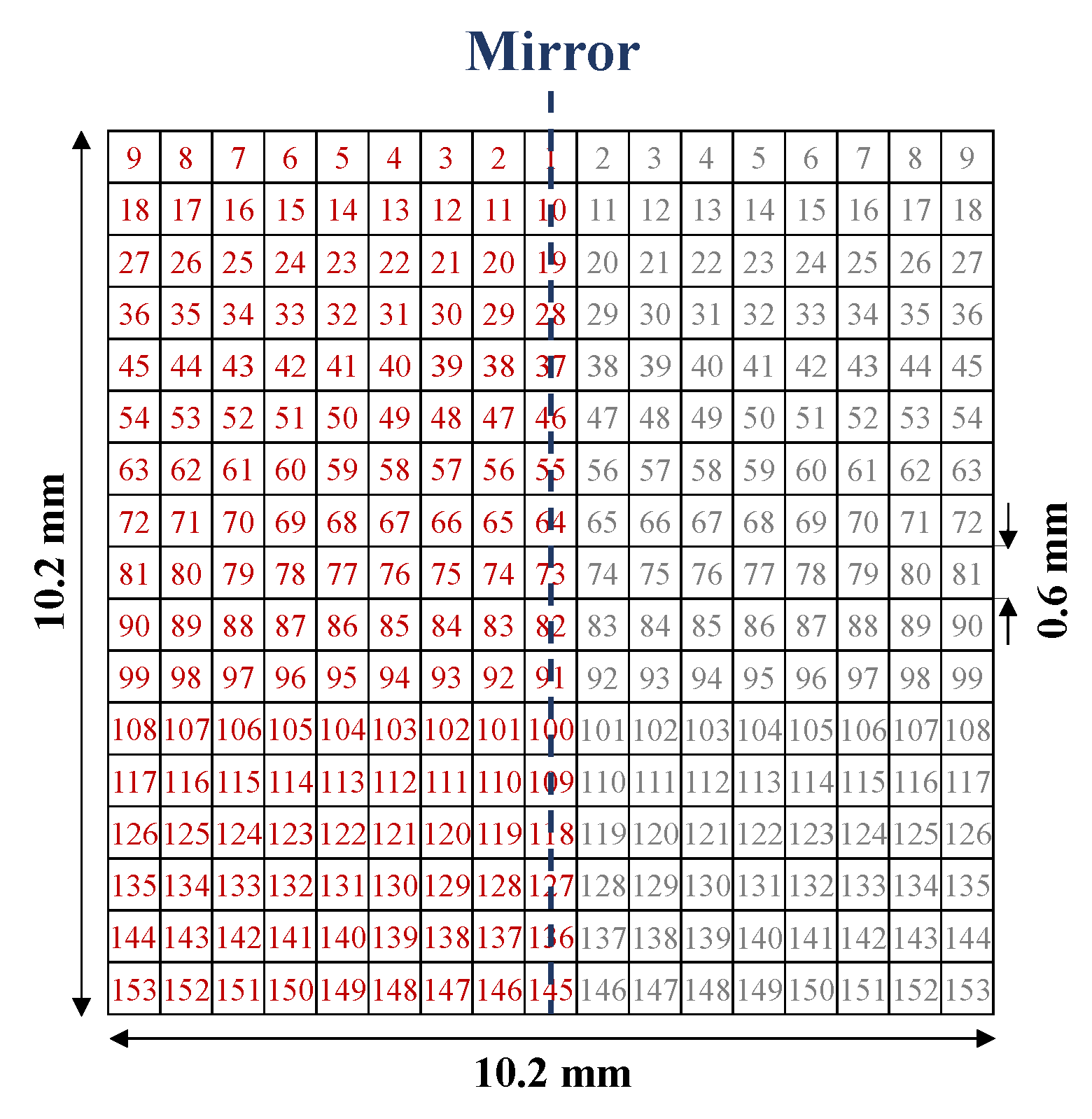
By assuming a microstrip line, a square of size 10.2 mm × 10.2 mm in the middle of the ground plane was considered as the sensing area (where the ESPR is etched) and was pixelated into
pixels, as shown in
Figure 18. Then, a binary value of 1 or 0 was assigned to each pixel so that each pixel was represented as a bit whereas having the value of 1 or 0 indicates the presence or absence of metal on the area of the pixel. In such a way, a string of bits represents the shape of the ESPR. Then, the binary version of the particle swarm optimization (PSO), namely BPSO [
86,
87], was applied to this string (such that each bit is an optimization parameter) to optimize the shape of the resonator for maximum sensitivity.
To reduce the number of independent bits (i.e., the number of optimization parameters) and thus achieve the faster convergence of the optimization algorithm, the design was constrained by enforcing a mirror symmetry with respect to an axis perpendicular to the feed microstrip line. Since setting initial value of the optimization parameters strongly impacts the convergence of every optimization method, to further accelerate the convergence, the initial values of the bits were set such that the initial shape of the resonator was a scaled version of the one used in [
88].
To maximize the sensitivity of the sensor to changes in the dielectric constant of the MUT, and since the change in the dielectric constant is sensed by the change in the resonance frequency (when loaded with MUT), the optimization cost function was defined as the inverse of the normalized resonance frequency shift () due to a material having . This choice was because of the characterization of the materials with a dielectric constant ranging between 1 and 10.
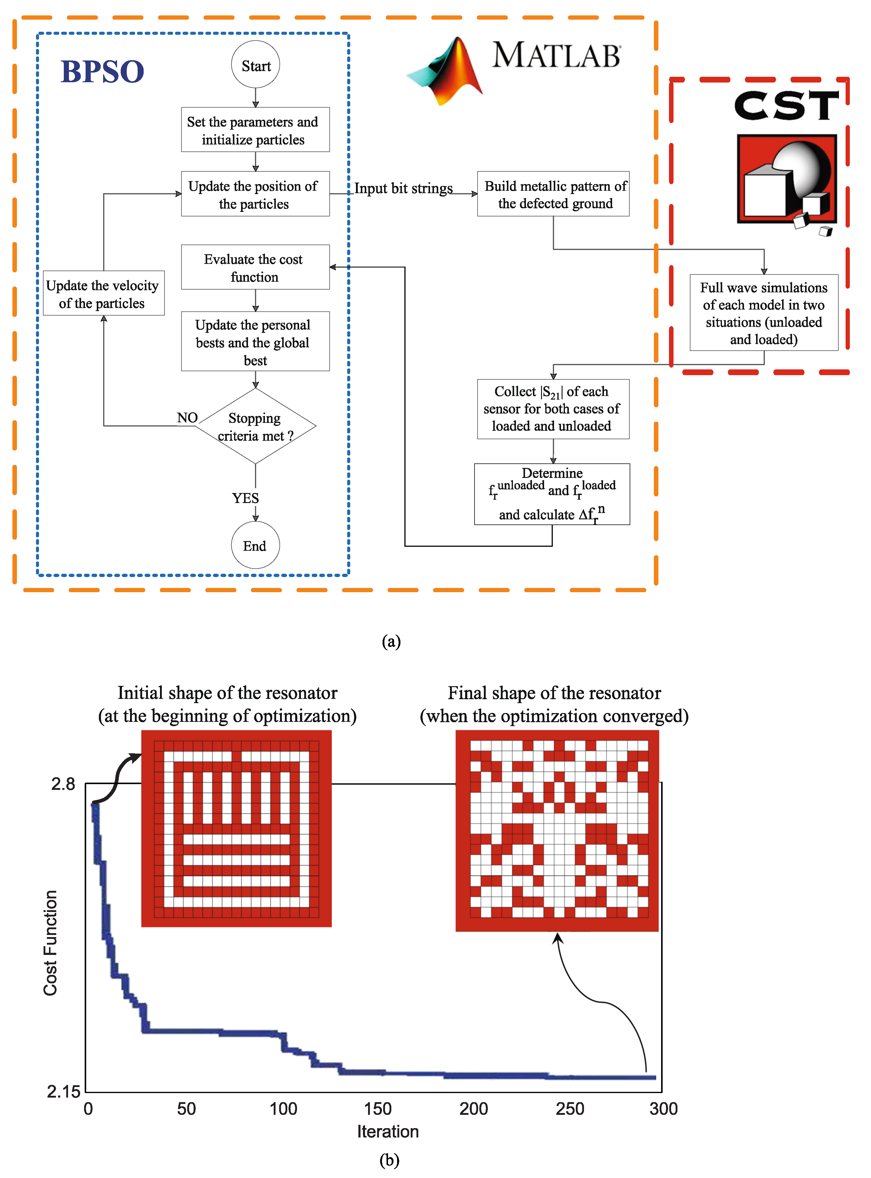
The process of optimizing the shape of the sensor was performed by writing a code in MATLAB and linking it to the CST as an electromagnetic full-wave simulator. The diagram of this process, including the flowchart of the BPSO algorithm and the relationship between MATLAB and CST, is shown in
Figure 19a.
In this process, after setting the initial parameters and generating binary strings, each string is converted to a pattern which can be simulated in CST. In CST, each model (sensor) is simulated when it is unloaded and when loaded with a sample having
. Then, the results of the full-wave EM simulations are fed back to MATLAB. Using the received transmission coefficients, the normalized resonance frequency shift of the loaded sensor (with respect to the unloaded state) is determined and the cost function is calculated.
Figure 19b shows the values of the cost function during the iterations of the algorithm indicating the decrease in the cost function from 2.78 (for the initial shape of the sensor) to 2.17 (for the final shape), or equivalently
was increased from 0.36 to 0.46. The pattern of the optimized sensor is shown in the inset of
Figure 19b.
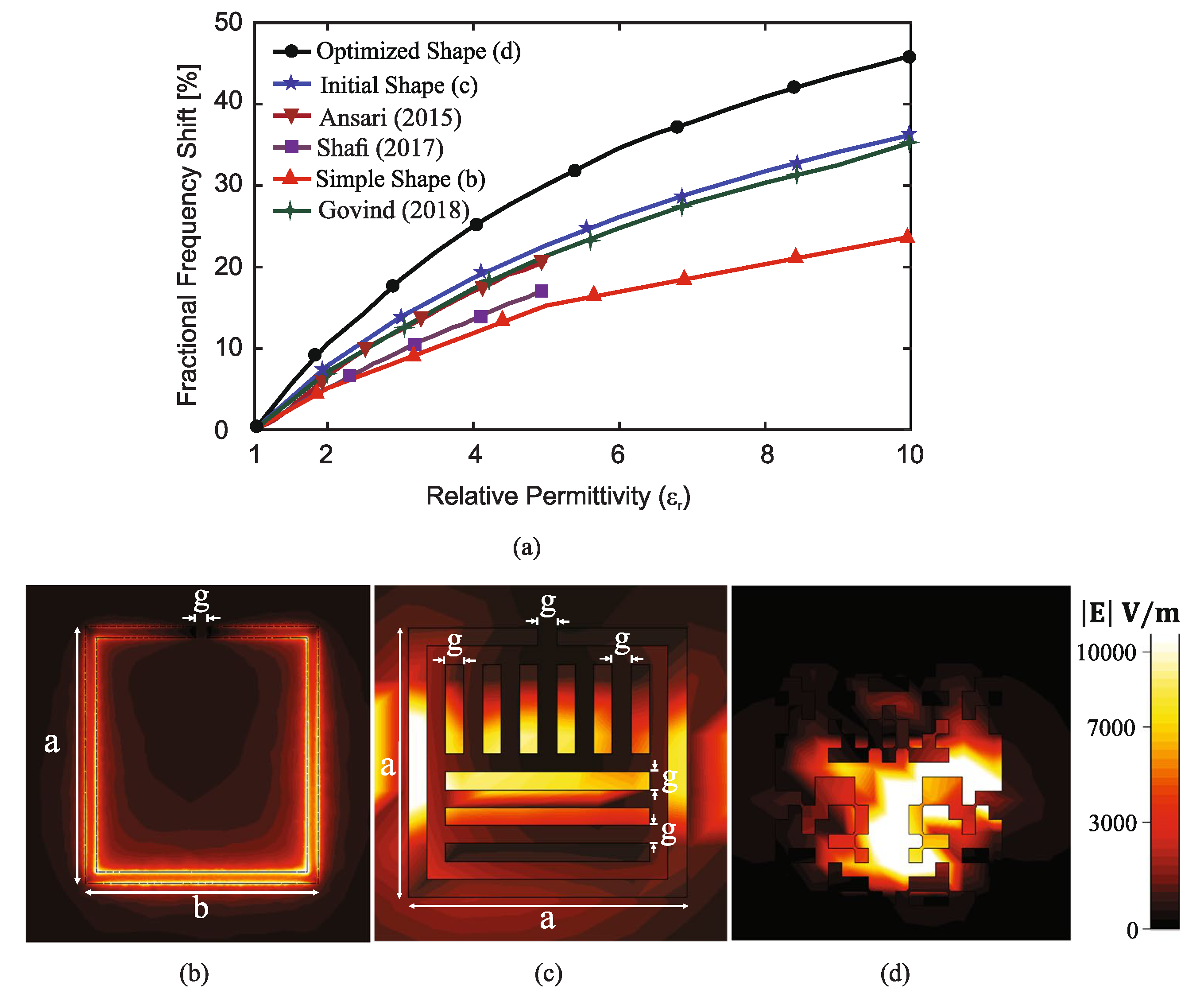
By gradually increasing the relative permittivity of the MUT from 1 to 10 in the simulations, in
Figure 20a, the normalized resonant frequency shift of the optimized sensor was compared with that of a simple CSRR sensor, the modified CSRR sensor which was considered as the initial state of the optimization, and those introduced in three other works (notice that the reference numbers in
Figure 20 shows the references of [
37]). It is evident that for every dielectric constant of MUT, the optimized sensor using pixelization and shape optimization exhibits the highest normalized resonant frequency shift. In particular, for dielectric constants of 2 and 10, this sensor shows normalized resonant frequency shifts of
and
. To understand the underlying mechanism behind this improvement,
Figure 20b–d show a comparison between the field intensity distributions on the simple CSRR, the resonator which was considered as the initial state of the optimization and the proposed shape-optimized resonator. From this comparison, it can be concluded that the sensitivity improvement in the pixelated sensor is due to (1) a stronger field on the sensing area such that the maximum intensity of the electric field is three times higher than that in
Figure 20c, and (2) a larger effective sensing area wherein the electric field has a strong intensity. These two features provide broader and more effective coupling (interaction) between the sensor and the MUT.
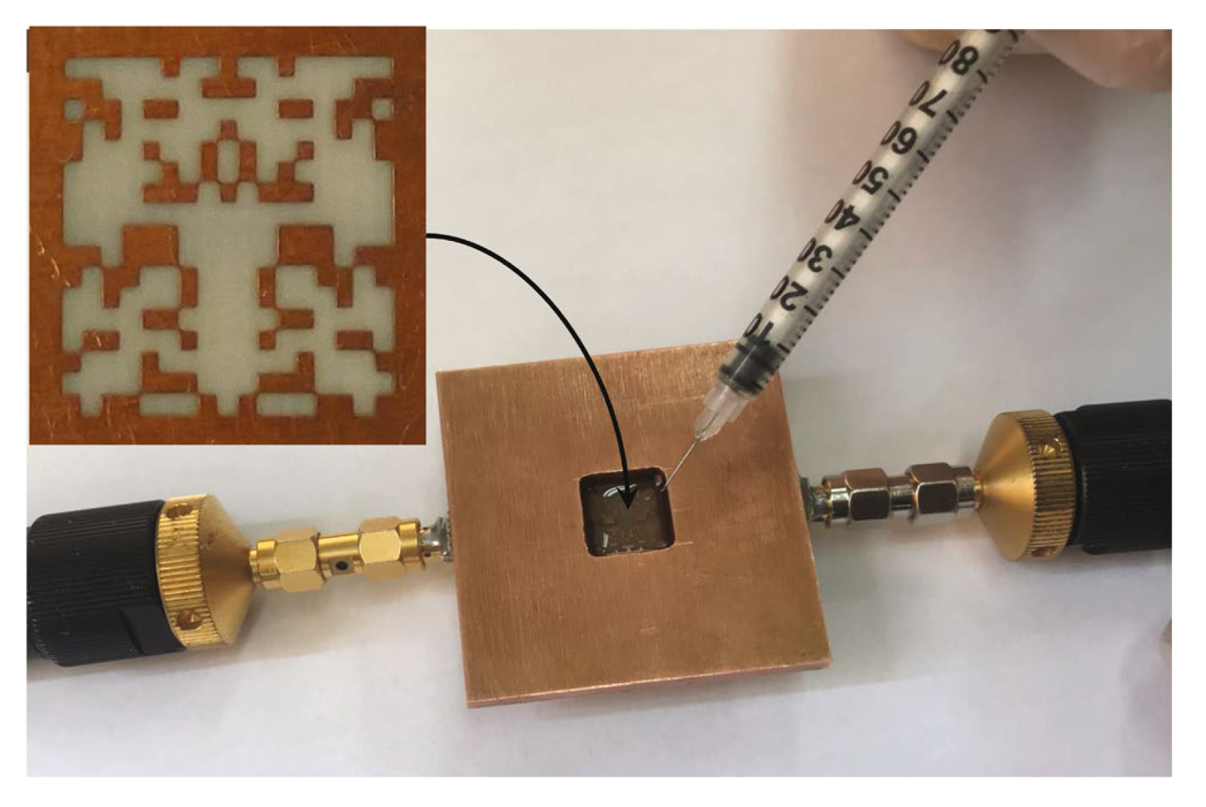
Experimental validation was also presented in [
37]. The optimized sensor was fabricated by etching the ground plane of a 50
microstrip line as shown in
Figure 21. A copper plate with a hole in the middle was placed on the ground plane of the board. The hole is slightly larger than the sensing area, thus effectively creating a small container that includes the sensor’s area in the bottom and an open top for inputting or pouring in the MUT. Two different tests were performed. In the first, the transmission coefficient (
) of the sensor when it was unloaded and was loaded with cyclohexane (
) and chloroform (
) having a known relative permittivity of 2.02 and 4.81 was measured. The measured and simulated transmission coefficients are seen in
Figure 22a–c, showing strong agreement between the simulations and experiments.
In the second set of experiments, the fabricated sensor was used to extract the dielectric constant of mixtures of chloroform and cyclohexane with different volume ratios. Each sample was tested with the optimized sensor and the transmission coefficient was measured and the normalized resonance frequency shift was obtained. Using the relation between the normalized frequency shift and the dielectric constant of the MUT (shown in
Figure 20), the relative permittivity of each mixture was obtained and compared with those approximated by the classic binary mixture and the Maxwell–Garnett formulas, as shown in
Figure 22d. Good agreement between the results is observed.
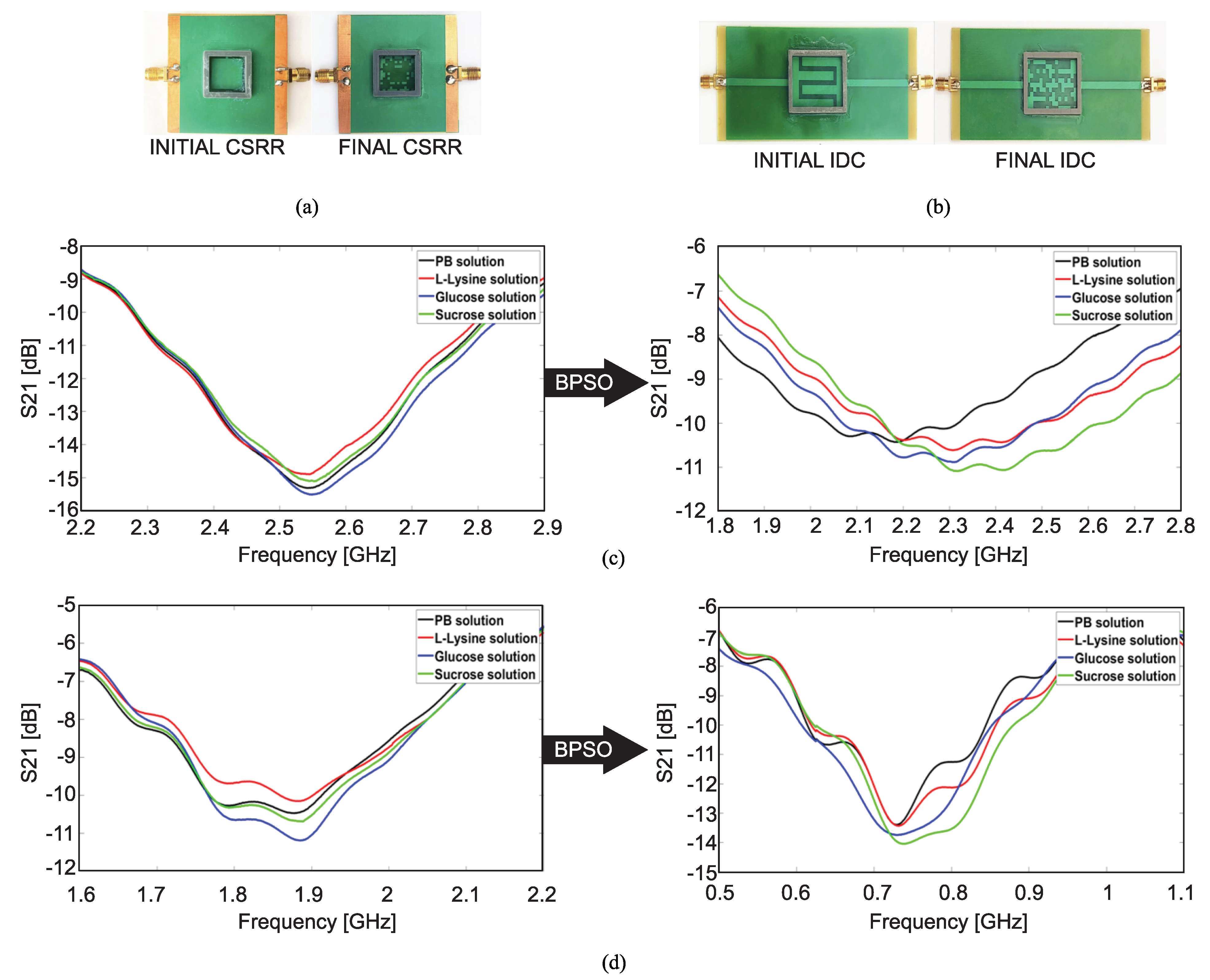
In a similar work [
84], the same approach, i.e., the pixelization of the sensing area (resonator area) and applying a binary optimization algorithm was used to design CSRR and interdigitated capacitor (IDC)-based sensors. While in the CSRR sensor, a resonator is etched on the ground plane of a microstrip line, in the IDC sensor, the resonator (which consists of inductive inter-digitated fingers with capacitive gaps between them) is placed between two sections of a microstrip line.
Figure 23a,b show the fabricated CSRR and IDC sensors before (the design which was given to the BPSO algorithm as an initial design) and after resonator shape optimization.
The sensors in this work were designed for bio-sensing applications, where most of the samples are dissolved in respective solvents. Hence, the normalized frequency shift was calculated with respect to a solvent which was a solution of 34 g of phosphate buffer (PB) in one liter of deionized water. This PB solution was used as the solvent of other samples: L-Lysine, glucose and sucrose.
Figure 23 shows the measured responses of the CSRR (a) and IDC (b) sensors before and after optimization (transmission and reflection coefficients in the cases of CSRR and IDC sensors, respectively). It is seen that the normalized frequency shifts after the shape optimization of the resonator increased in both cases, which is identical to sensitivity improvement.
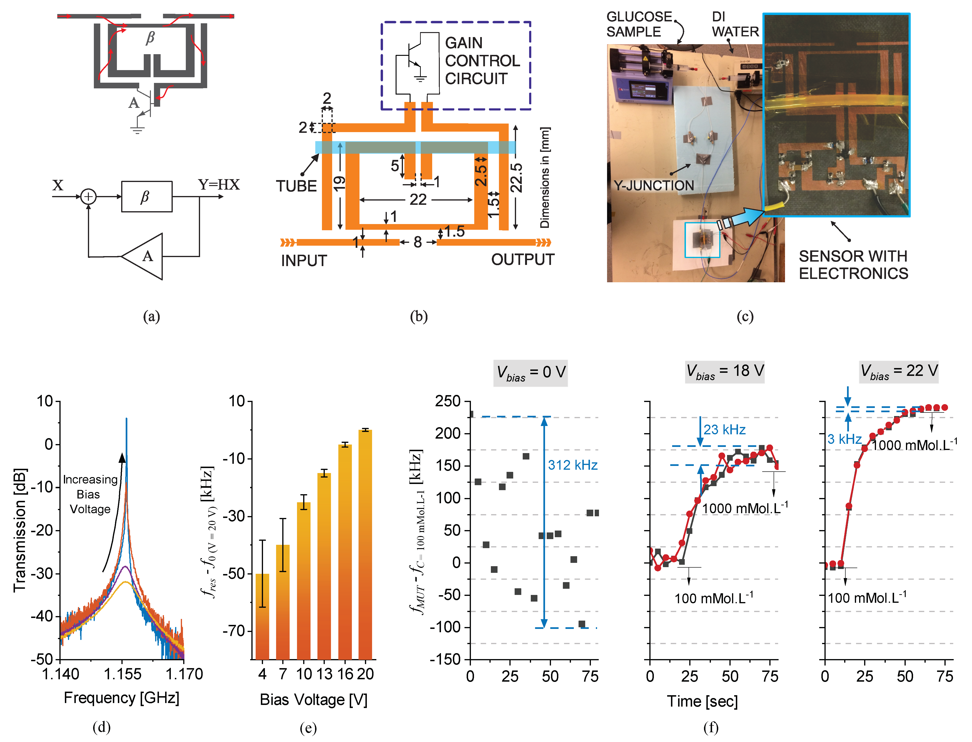
In the two aforementioned works [
37,
84], the optimum shape of the resonator was obtained by applying a binary swarm optimization. Although the swarm intelligence algorithms are easy to implement, for large-scale and fine-grained optimization problems, the demands of the number of dimensions and the population of the solution are high, resulting in a slow modeling speed and high iteration number. To address this problem, in [
85], deep reinforcement learning was applied to optimize the shape of the resonator etched on the ground plane of a microstrip line in a microwave microfluidic sensor.
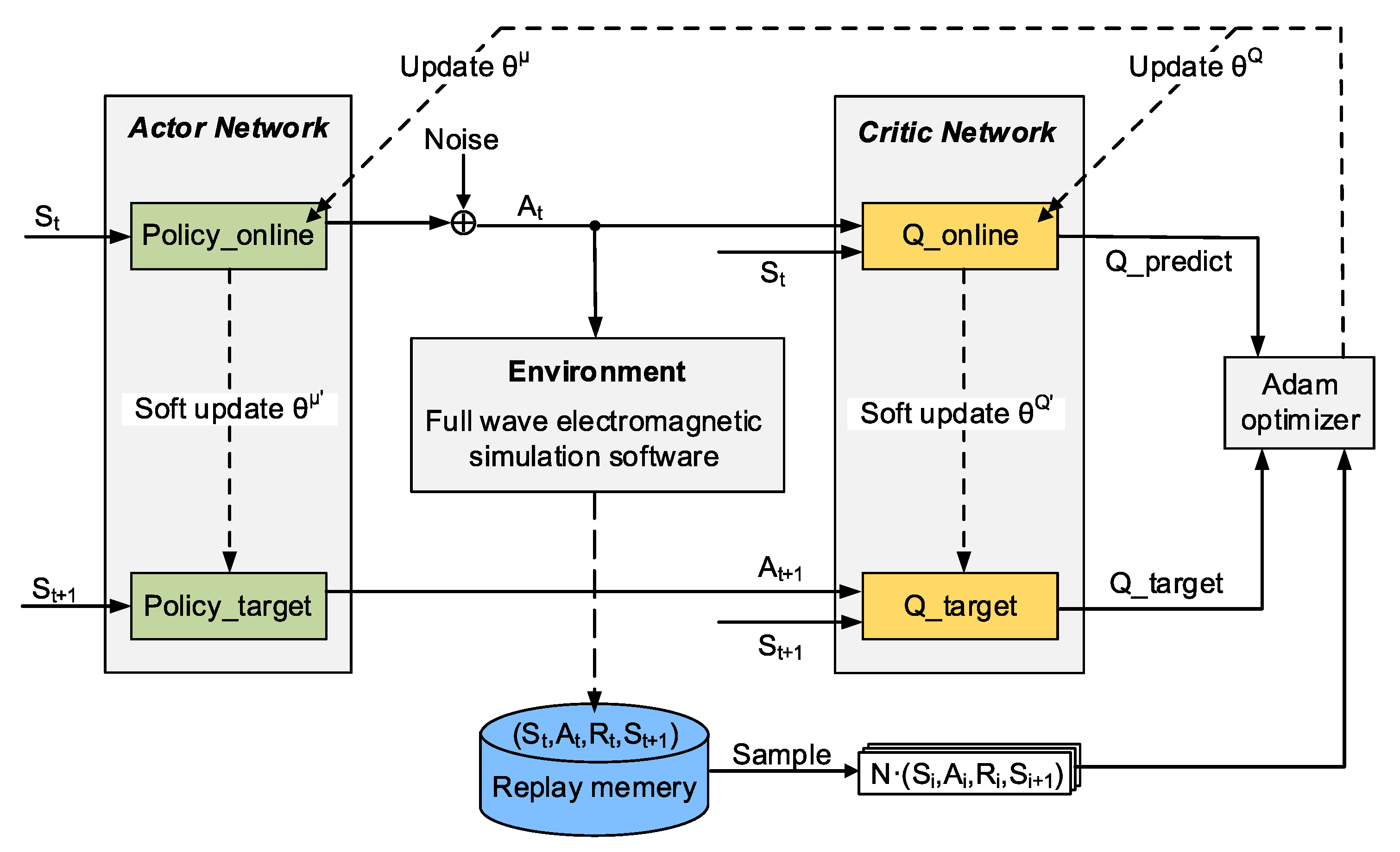
A deep deterministic policy gradient (DDPG) [
92] framework, as shown in
Figure 24, including actor and critic networks (both are neural networks) and a full-wave electromagnetic simulator (HFSS), was employed as an agent for learning an optimization strategy. In this strategy, as shown in
Figure 25, by considering one-axis symmetry for the resonator, half of the resonator area was pixelated, and a bit of 0 or 1 corresponding etched or unetched was assigned to each pixel. Therefore, a string of bits shows the state space. The agent would determine a series of structural adjustment actions according to the current state and the learned knowledge. The agent would receive a reward according to the state and action. As the goal of the optimization was to find out the resonator structure with the largest relative resonant frequency shift (i.e., the optimal sensitivity) when loaded with the samples through a series of action adjustments, the main reward factor is the relative resonant frequency shift of the loaded sensor. Meanwhile, the normalization of the microfluidic channel was also considered as the channel which is bonded onto the resonator structure. The incorrect actions that make the microfluidic channel difficult to fabricate or affect the liquid flow were defined, and a penalty was considered for them in the reward function.
The optimization procedure of the DDPG agent can be described as follows. The agents would gradually learn in the process of continuous interaction with the simulation environment. As such, the agent chooses the actions to adjust the resonator structure, the model script generated by the program is constructed in the electromagnetic simulation software and the simulated results are used as the output to evaluate the performance of the resonator structure. Then, the program provides the reward value and goes to the next episode until the actor and critic networks eventually converge. The optimal solution could be obtained and output as the optimal resonator structure of the microwave microfluidic sensor.
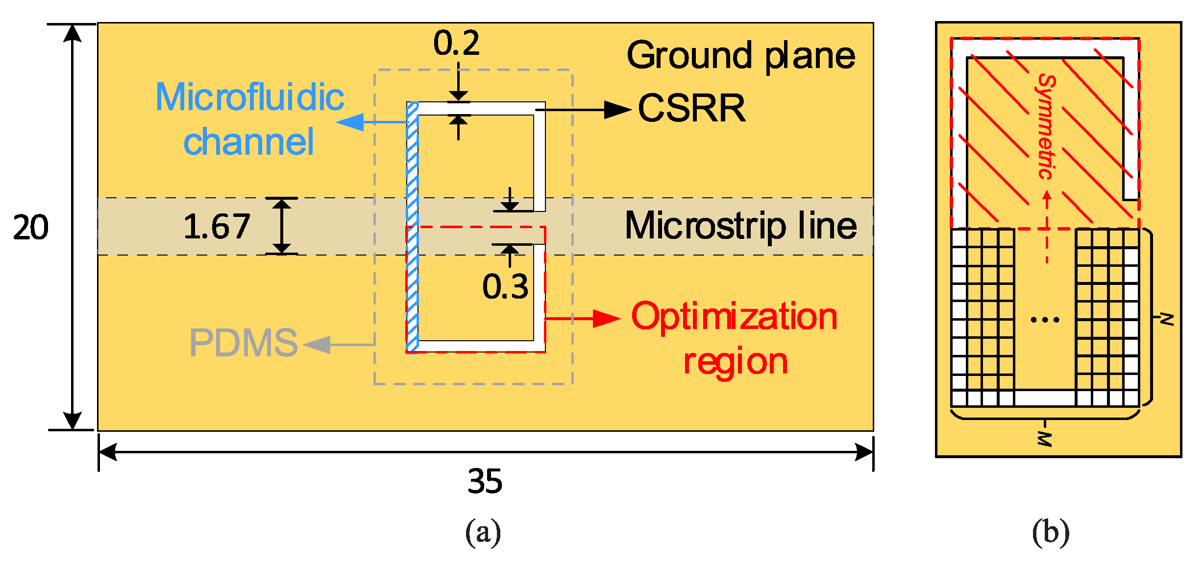
A classical complementary split-ring resonator structure (shown in
Figure 25) was used as an initial structure and optimized in two ways, i.e., with and without a fixed liquid volume consumption. In the former optimization, the goal was to maximize the relative resonant frequency shift when the volume of the fluid sample under test was fixed to 2.4
L. However, in the latter, the goal was to maximize the resonance frequency shift and minimize the sample volume at the same time. As a result, a liquid volume of 0.8
L was needed for the optimized sensor in the second way.
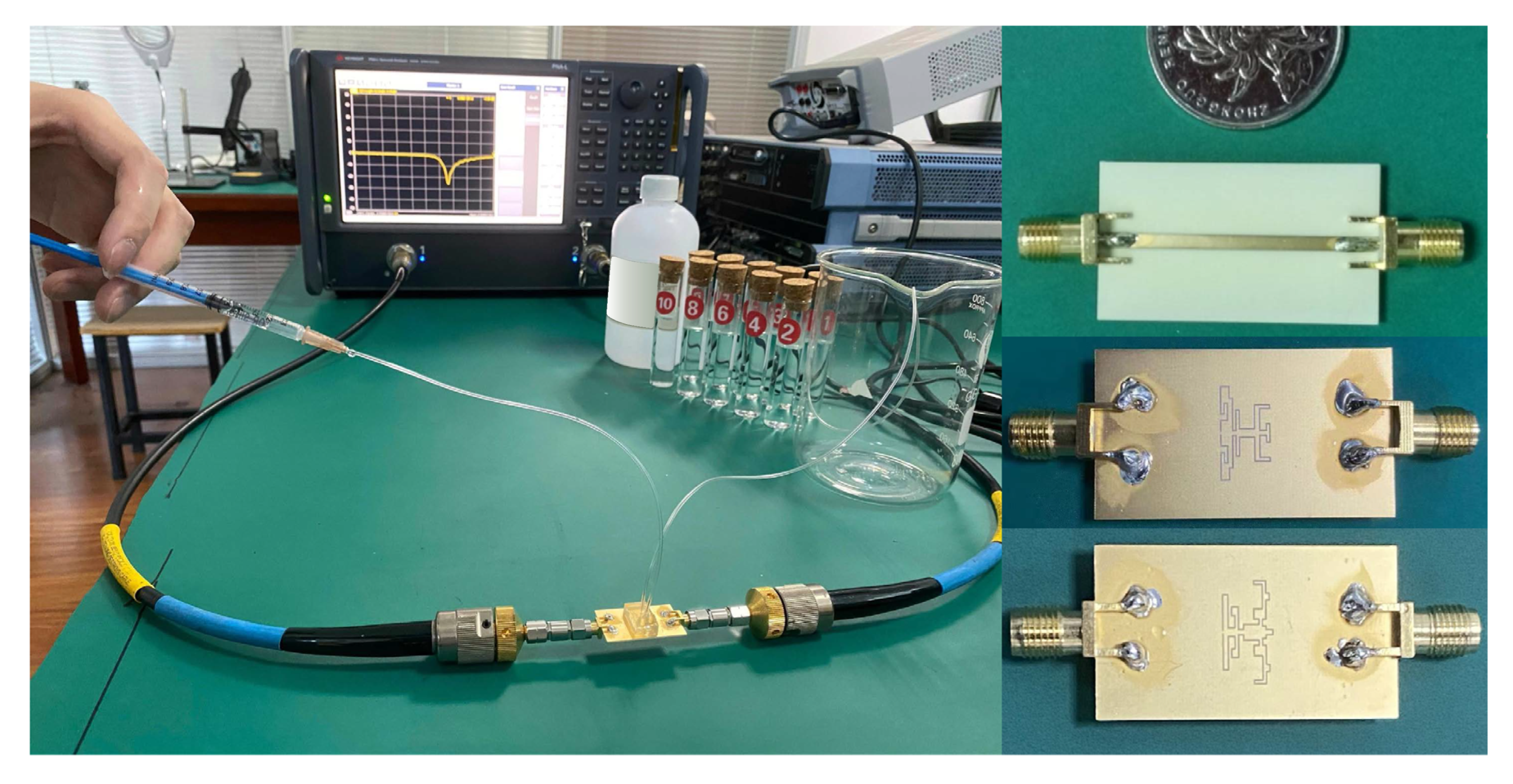
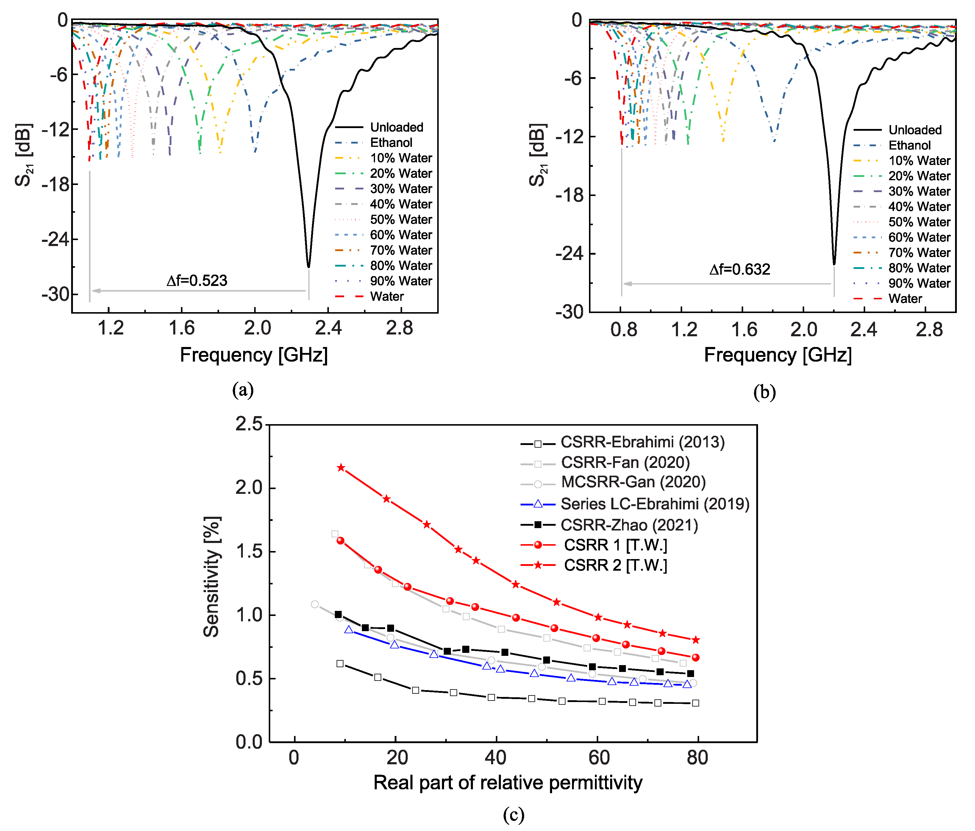
As shown in
Figure 26, the optimized sensors were fabricated and tested with water–ethanol solutions in different ratios as the samples under test. The transmission responses of the sensors in their unloaded and loaded states are given in
Figure 27a,b.
By defining the sensitivity as
Figure 27c compares the sensitivity of the sensors proposed in [
85] with that of some other CSRR-based sensors (the reference numbers are for [
85]). Considerable improvement of the sensitivity is observed.
2.6. Incorporating Phase Variation
In this subsection, a strategy to significantly enhance the sensitivity in phase-variation microwave sensors is reviewed. Such a technique is applied to one-port reflective-mode sensors, where the sensing element is a resonant element, either distributed or semi-lumped, and it consists of cascading to a sensing element such as a set of quarter-wavelength transmission line sections with alternating high and low impedance [
96,
97,
98,
99]. The considered phase-variation sensors operate at a single frequency, and their canonical output variable is the phase of the reflection coefficient, whereas the natural input variable is the dielectric constant of the material under test (MUT), which should be in contact with the sensing element. The simplest implementations of phase-variation sensors consist in a one-port (reflective-mode) [
39,
96,
100,
101,
102,
103] or a two-port (transmission-mode) [
38,
104,
105,
106] transmission line, the sensing element. When a material is in contact with the line, the effective dielectric constant of such a line is modified, and consequently, the phase velocity and the characteristic impedance are also altered. The result is a variation of the electrical length of the line and, ultimately, a variation in the phase of the reflection (reflective-mode) or transmission (transmission-mode) coefficient of the line is also generated. The electrical length of the line is given by
where
is the phase constant of the line and l its length,
and
being the angular frequency and the phase velocity, respectively. Although
is not the typical output variable (it only coincides with the phase of the transmission coefficient of the line in matched lines), from (
22), it can be easily deduced that the variation of the phase (electrical length) of the line with the dielectric constant of the MUT, the input variable, will increase by increasing either the frequency or the length of the line, or both. Thus, it can be concluded that the sensitivity (or derivative of the output variable, the phase of the reflection or transmission coefficient, with the dielectric constant of the MUT) increases with the operating frequency or with the line length. Indeed, highly sensitive sensors based on long (typically meandered) sensing lines have been reported [
105,
106]. However, this obvious strategy has the penalty of large sensing regions, provided that a high sensitivity is required. Increasing the operating frequency, the other canonical sensitivity enhancement strategy in phase-variation sensors, is not always applicable (sometimes, the operating frequency is dictated by external factors), or, if applicable, it may represent an increase in the cost of the associated electronics for signal generation and processing in a real scenario. To enhance the sensitivity in one-port phase-variation sensors, a novel strategy was pointed out in [
96]. In the simplest form, the sensor consists of an open-ended line with impedance
and electrical length
(at the operating frequency) when the line is loaded with the reference material (e.g., air), as can be seen in
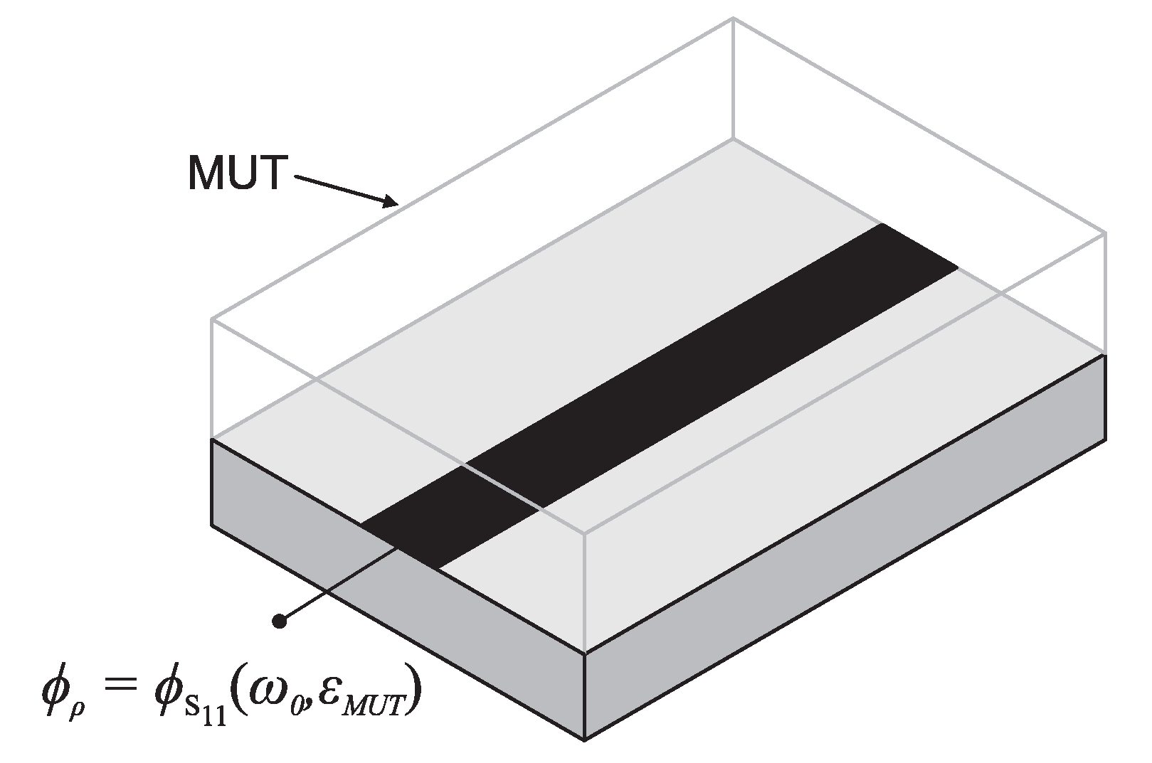
Figure 28.
The output variable is the phase of the reflection coefficient,
, which varies when a material under test (MUT) is in contact with the line. To obtain the dependence of such an output variable with the parameters of the line, it is first necessary to infer the impedance seen from the input port, given by [
52,
96]
The reflection coefficient is thus
and the phase of the reflection coefficient is therefore
The sensitivity can be expressed as:
where the different derivatives appearing in (
26) are given by
The derivatives (
29,
30) correspond to a microstrip sensing line,
and
F being the effective dielectric constant and the form factor as defined in [
52,
107], respectively, (for CPWs, the same expressions apply, but forcing the geometry factor to be null,
F = 0). Introducing (
27) in (
26), the sensitivity can be expressed as
As demonstrated in [
52,
96], the sensitivity in the limit of small perturbations is optimized by choosing
and
as high as possible (as compared to
), or alternatively, by forcing
and
as low as possible. In the former case, the sensitivity is given by
In the second case (
and
low), the sensitivity is calculated as
According to (
32) and (
33), it is clear that the sensitivity is enhanced by considering the sensing lines with a high index
n, that is, many (odd) multiples of a quarter-wavelength, or many multiples of a half-wavelength, depending on the ratio between
and
. However, with this strategy, the length of the sensing line may be excessive. In [
96], it was demonstrated that by simply alternating between cascading high- and low-impedance quarter-wavelength transmission line sections, the sensitivity can be substantially enhanced (see
Figure 29).
For
and high-impedance sensing lines, the
line section adjacent to the sensing line must exhibit a low characteristic impedance, whereas for
and low impedance sensing lines, the characteristic impedance of the quarter-wavelength line section cascaded to it must be high. If the impedances of such high/low
lines are designated with the variable
, where
i indicates the position of the line section (with
corresponding to the line adjacent to the sensing line), the sensitivity can be expressed according to four cases, depending on whether the total number of quarter-wavelength high/low-impedance line sections,
N, is odd or even, that is [
52,
96]:
Case
and
N odd.
Case
and
N odd.
Case
and
N even.
Case
and
N even.
To illustrate the potential of this approach, based on a
or a
sensing line and a step impedance configuration,
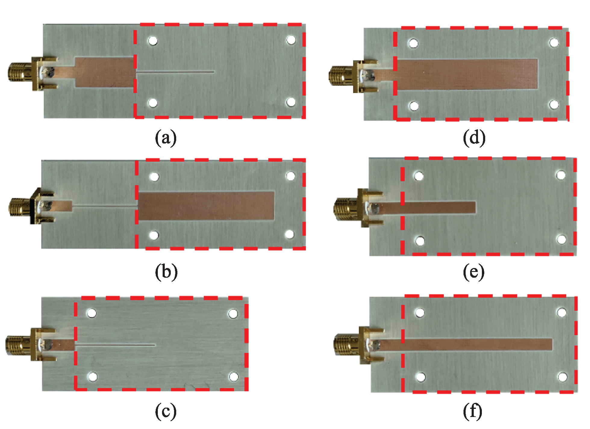
Figure 30 shows the photograph of different sensors, whereas
Figure 4 depicts the phase variation of the reflection coefficient with the dielectric constant of the MUT and the sensitivity [
96]. Note that the considered reference MUT is air, which means that the electrical length of the sensing lines (either
or
, depending on the case) is for the bare sensing line at the considered operating frequency (
). The impedance
of this line is also for the bare sensing line. The sensitivities in the limit of small perturbations are indicated in
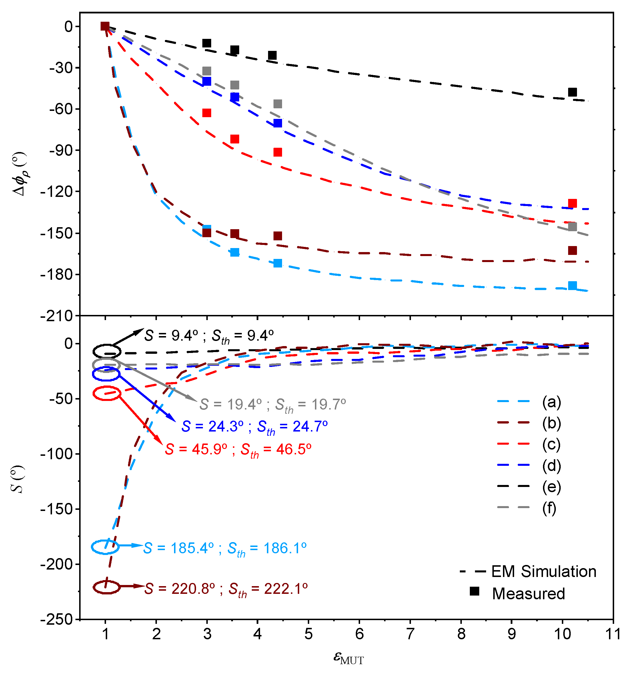
Figure 31 for each sensor, and it can be seen that they coincide to a good approximation with the theoretical sensitivities (
in the figure), as inferred from expressions (
34)–(
37). For sensors (a) and (b), the sensitivities in the limit of small perturbations are very high, but it should be mentioned that such high sensitivities are achieved at the expense of degradation in the sensor linearity. Thus, these highly sensitive phase-variation sensors are of special interest in applications where the measurement of small perturbations in the input variable with regard to the reference one should be measured. Although these sensors are canonically permittivity sensors, the input variable can be any other variable related to the permittivity, for example, the level of concentration of solute in diluted solutions, or even other variables such as temperature or humidity, which can modify the dielectric constant of certain materials [
52]. Let us also mention that, with these high sensitivities, these sensors are very interesting for the detection of tiny defects in samples, which typically manifest as variations in the effective dielectric constant of the sample.
In the reported implementations of
Figure 30, the sensing elements are
or
open-ended lines, i.e., distributed resonators. However, such distributed resonators can be replaced with electrically small semi-lumped resonators, as demonstrated in [
39], where a reflective-mode phase-variation sensor based on an open complementary split-ring resonator (OCSRR) terminating a step impedance CPW structure was reported. It has also been demonstrated that this type of phase-variation sensor is useful for the measurement of short-range displacements [
108] and can be also useful for the measurement of liquid levels.
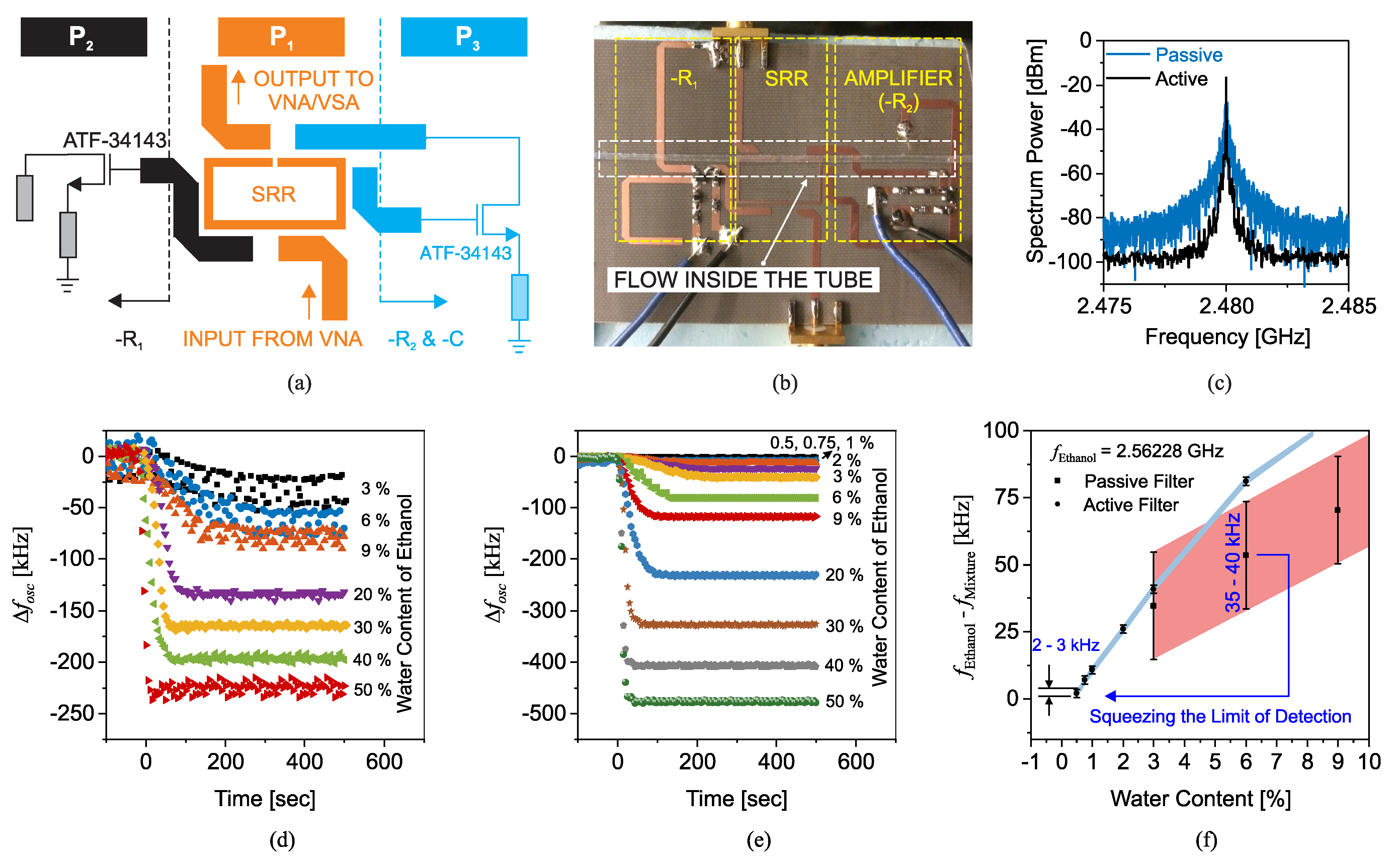
2.7. Exploiting the Coupled-Line Sections
It has been shown that coupled line sections are applicable for high-sensitivity dielectric sample detection. The idea of using a coupled-line section as a dielectric constant sensor was first proposed by Piekarz et al. in 2015 [
40] and then developed in their subsequent works [
109,
110]. The main thought behind their studies was to exploit the odd-mode characteristic impedance of a coupled line section. This is because putting a dielectric sample on the top of a coupled-line section significantly influences its odd-mode characteristic impedance, which is related to the mutual capacitance between coupled strips, not merely the capacitance between the strips and the ground plane as in a single section microstrip line.
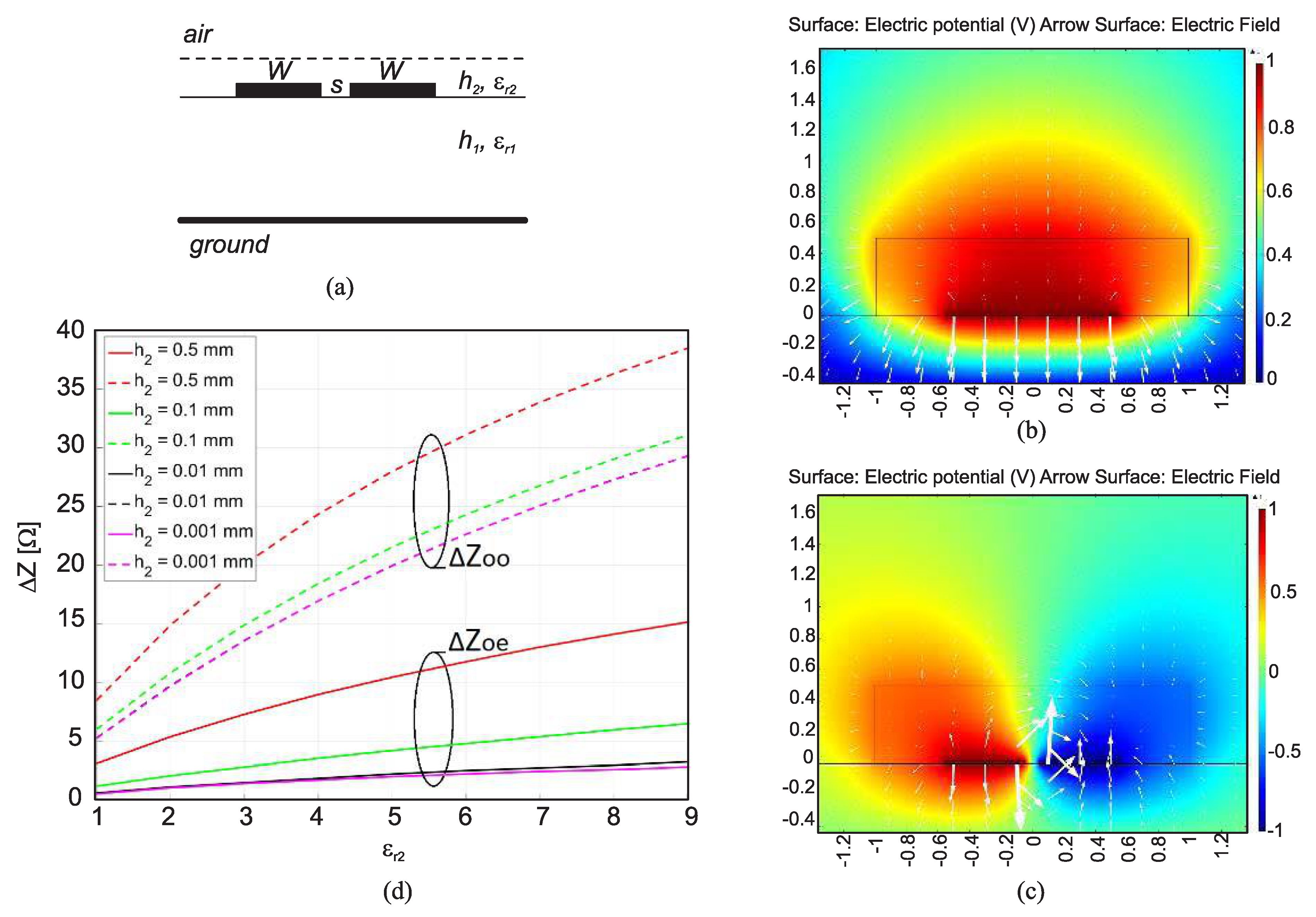
Figure 32a shows a microstrip coupled-line section covered with a dielectric sample.
Figure 32b,c depict the electric voltage (colors) and field (vectors) distribution in the cross-section for the even and odd modes excitation, respectively, (i.e., when the two lines are excited in phase and out of phase with the same amplitude). It is clear that the field is within the substrate for the even mode excitation, while in the case of odd mode excitation, the field is partially within the dielectric sample above the line. Therefore, the coupled lines’ odd-mode impedance exhibits a much higher sensitivity on the dielectric cover than the even-mode impedance, as observed in
Figure 32d different thicknesses and the permittivities of the covering material. Moreover, the sample can be as narrow as the distance between the coupled lines due to the field distribution, shown in
Figure 32c.
In their first work [
40], as shown in
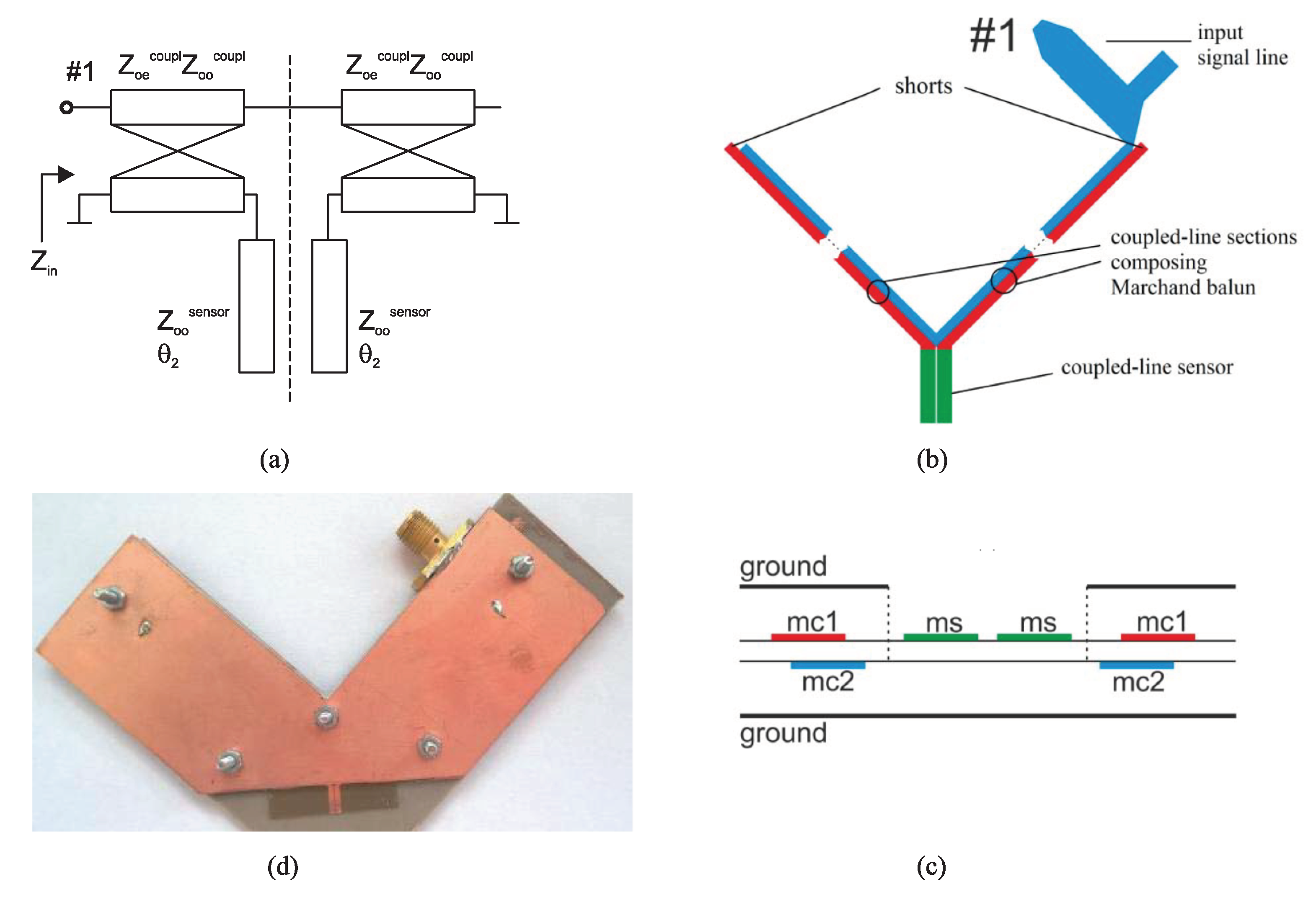
Figure 33, Piekarz et al. used a Marchand balun to excite an open-ended coupled-line sensor out of phase in a wide-band. The Marchand balun was designed based on broadside-coupled stripline, as can be seen in
Figure 33b. The measurement setup, including the Marchand balun and the open-ended coupled-line section (sensor), is shown in
Figure 33c. The material under test is placed on the sensor and the characterization mechanism is as follows. First, the reflection coefficient at port 1 (see
Figure 33a) is measured, and its input impedance is obtained. Then, using analytic relations, the input impedance of the sensor section (open-ended coupled-line section), namely the load impedance, is calculated. Notice that since the balun on the differential ports excites the coupled-line section in its odd mode, the load impedance only depends on the odd mode characteristic impedance and the electrical length of this section. Subsequently, after some mathematical manipulations, the odd-mode effective dielectric constant can be calculated using the obtained load impedance and the odd-mode per-unit-length capacitance of the unloaded coupled-line sensor determined during the calibration process. It should be noted that this procedure does not give the dielectric constant of the MUT but the odd-mode effective dielectric constant of the coupled line section, which is between the dielectric constants of the MUT and substrate.
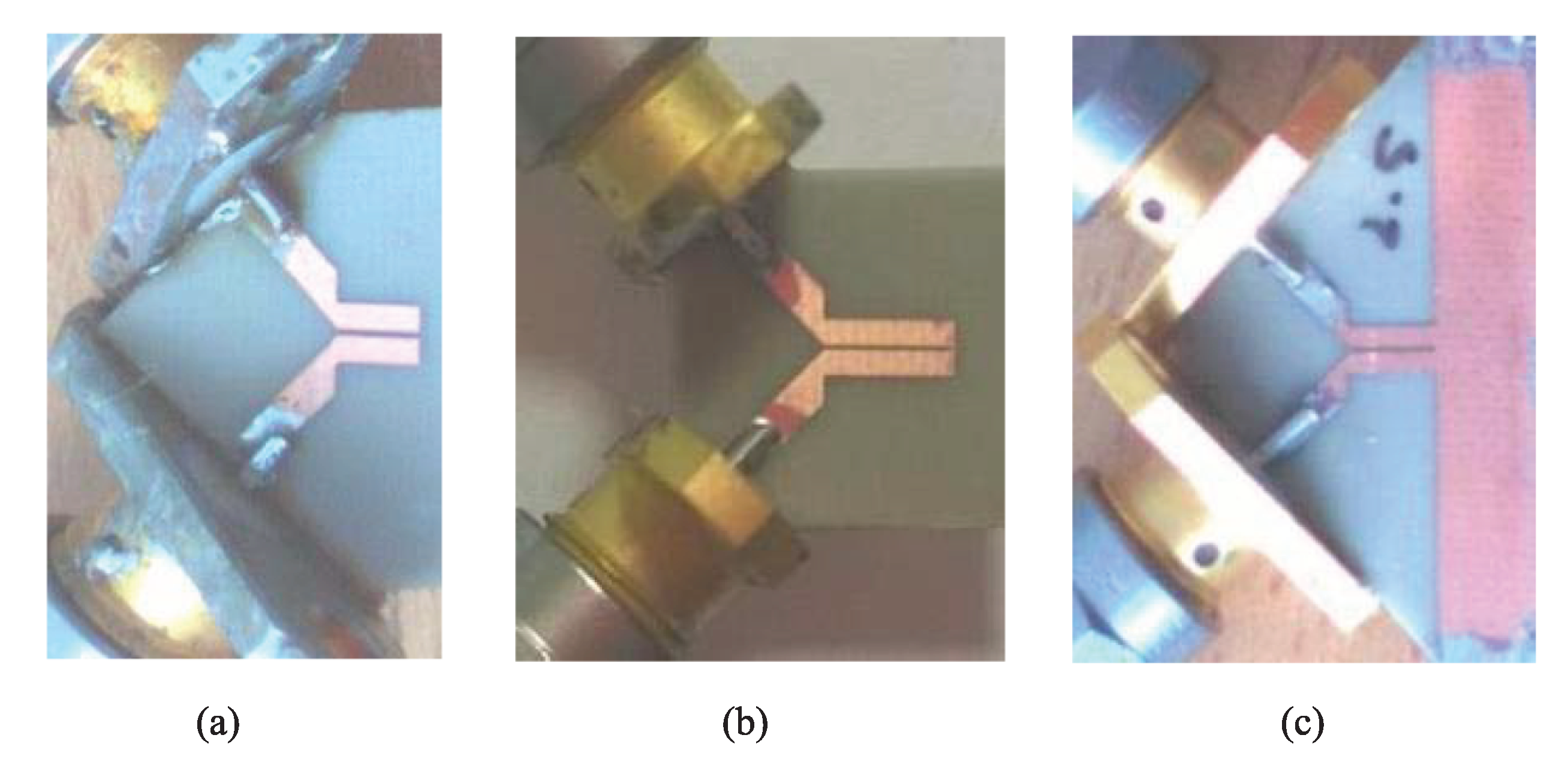
In their second work, the same authors removed the need for Marchand balun and performed two-port single-ended S-parameter measurements of the coupled line section. The differential input impedance of the sensor (i.e., the input impedance of the section for the odd mode excitation) was calculated from the two-port S-parameters, then, following a procedure similar to their first work, the odd-mode effective permittivity was obtained. As an advancement over their first work, the odd-mode effective permittivity of the coupled line section was finally converted to the complex permittivity of MUT using an electromagnetic (EM) simulation tool in an iterative procedure. In addition, in the newer work, not only an open-ended coupled line section but also short-ended sections where the two coupled lines were connected with a small metallic segment or a large grounded pad were theoretically and experimentally investigated. The three fabricated sensors are depicted in
Figure 34. It has been shown that the short-ended sensors have better accuracy for high frequencies (still in the low gigahertz regime), while the open-ended section is suitable for characterizing samples, which feature relatively significant permittivity change for the lower frequencies. Moreover, the calibration process is easier for the sensor shown in
Figure 34c, i.e., when the two coupled lines are connected using a grounded pad.
In the most recent work of the same group [
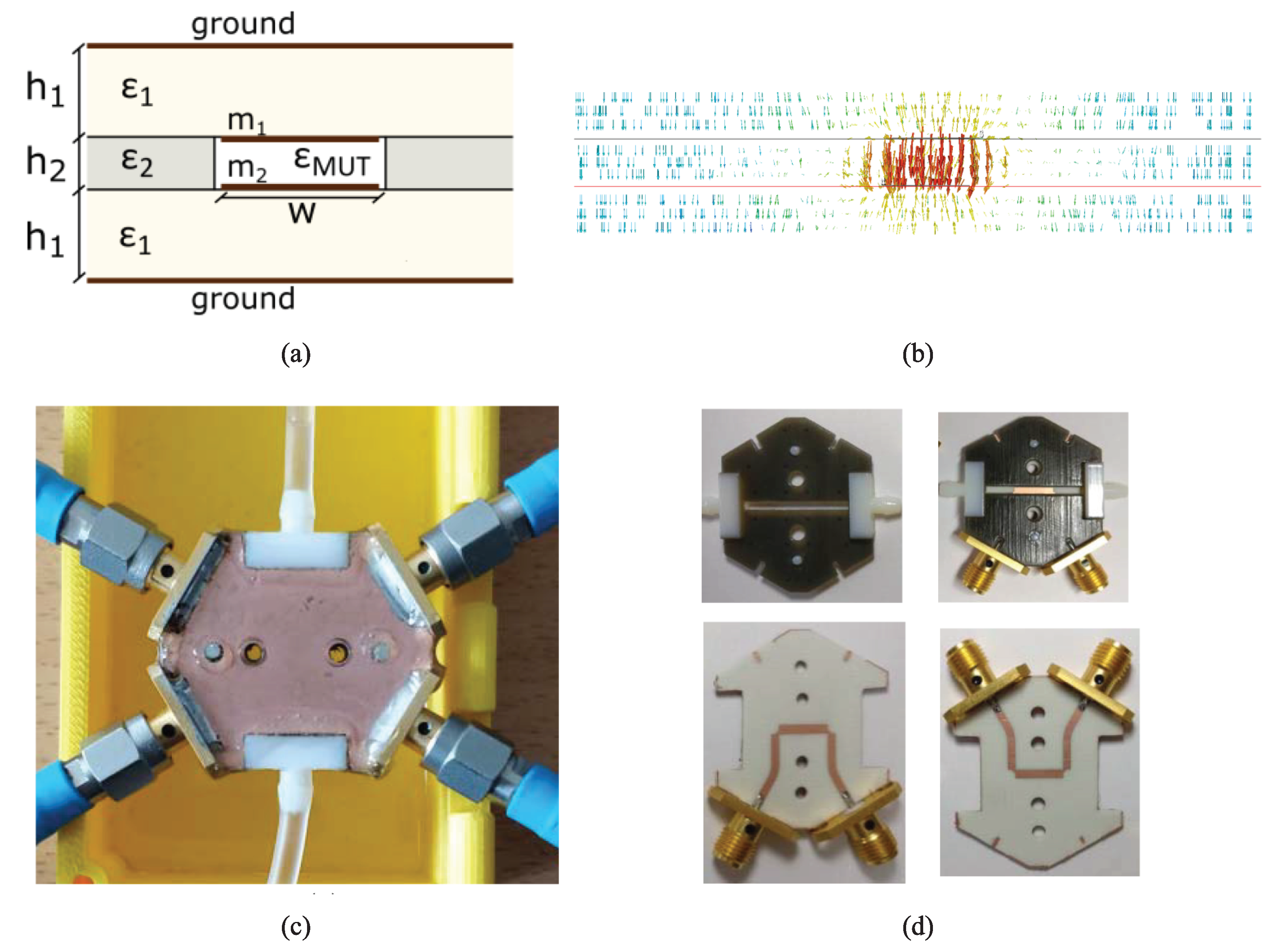
110], as shown in
Figure 35a, a four-port broadside-coupled line section based on a stripline was utilized to determine the dielectric constant of liquid samples. A microfluidic channel was realized using 3D printing technology in between the two aligned coupled strips.
Figure 35b shows the electric field distribution within the cross-section of the broadside-coupled-line section under a differential excitation. As can be seen, unlike the field distribution in an edge-coupled line sensor (shown in
Figure 35c) in the broadside-coupled-line sensor, the field is confined within the sample volume (between the two strips); hence, a higher sensitivity. Moreover, in the broadside-coupled-line sensor, the odd-mode effective permittivity is identical to the permittivity of the MUT. Therefore, the need for a computer simulation-based procedure to convert the effective permittivity to the permittivity of the MUT was removed. Experimental validation was presented by fabricating the sensor and performing four-port measurements for various liquid samples in the low-gigahertz regime, as shown in
Figure 35c,d.
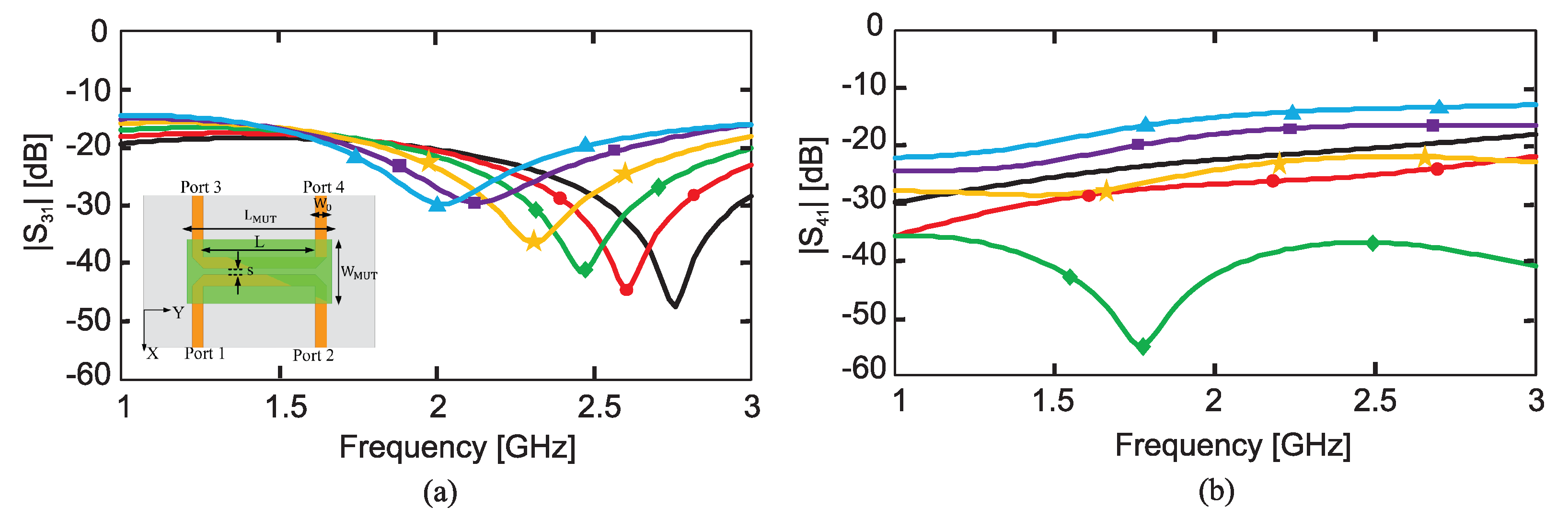
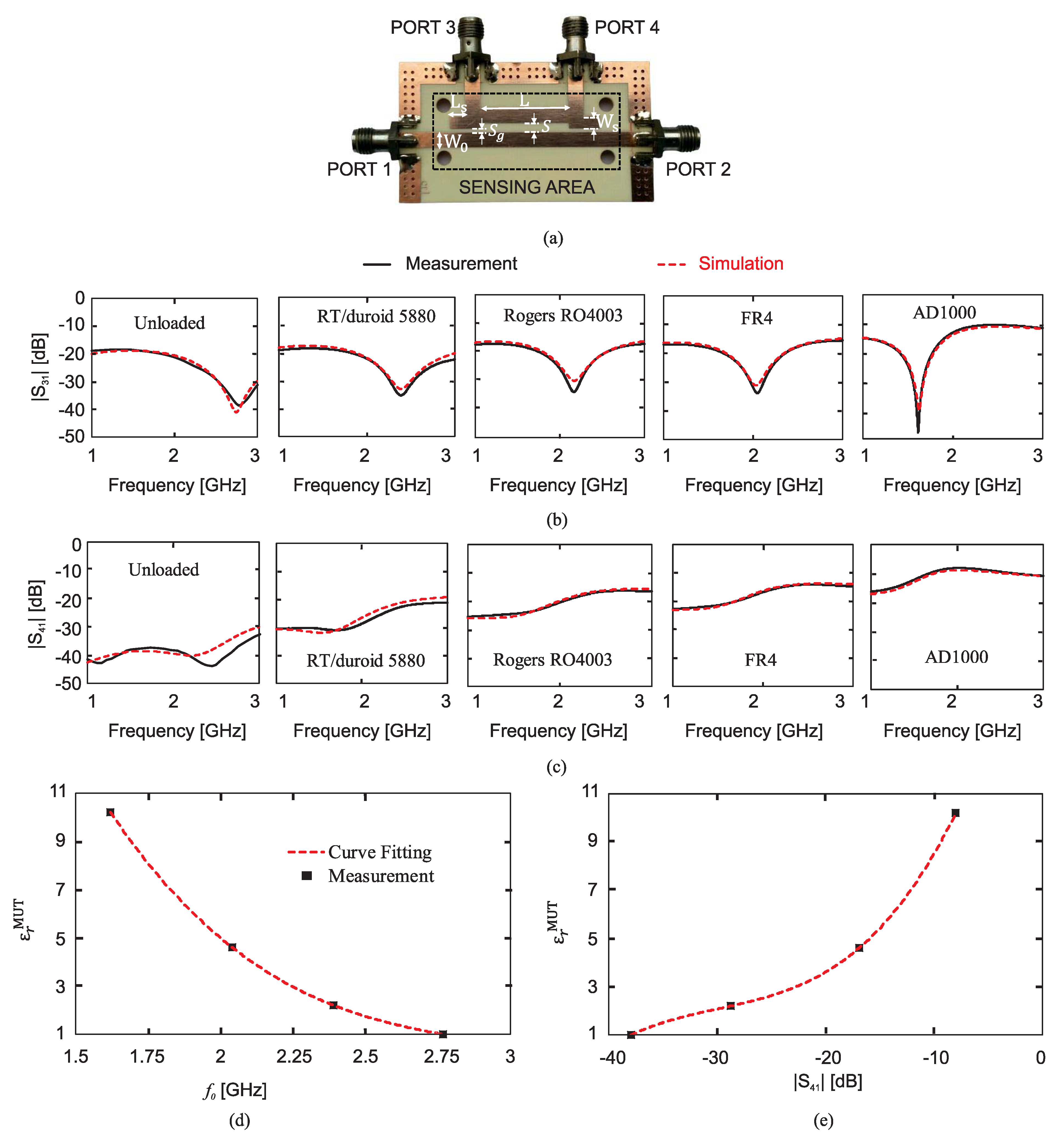
Another recent work proposed utilizing a high-directivity microstrip coupled-line directional coupler (with the through port terminated to a match load) for dielectric constant measurements in the low gigahertz regime. The MUT was placed on the coupled-line section of the coupler, and either the coupler’s coupling (
) or its isolation level (
) was considered as the sensor’s response. The idea behind this work is that putting different MUTs on the coupled line section leads to a change in the coupling coefficient and the isolation level of the coupler. It is noticeable that while, in the works of Piekarz et al. [
40,
109,
110], VNA measurements were required for the odd-mode impedance extraction, and [
111] only needs the amplitude of one transmission coefficient; hence, there is no need for a VNA, but instead, either a scalar network analyzer or a frequency synthesizer and a power detector, which make the measurements simpler and lower cost.
Figure 36a shows the simulated
for a simple microstrip directional coupler loaded with different MUTs. In this figure, the zero-coupling frequency of the coupler (
at which
is minimum) is
in the unloaded state (where
). According to the transmission line theory, zero coupling occurs at the frequency where the effective electrical length of the coupled line section equals an integer number of
. By increasing
from 1 to 10,
and consequently the effective electric length of the coupled line section increased, and as a result,
decreased from
to
, as can be seen in
Figure 36a. From this figure, it was concluded that
can be uniquely retrieved using
.
Figure 36b shows the isolation level (
) of the coupler for different values of
. However, ref. [
111] aimed to use
to detect
by increasing
, and the trend of
did not monotonically increase or decrease, making the unique extraction of
impossible. To resolve this problem, by adding two stubs at the ends of the coupled-line section, as shown in
Figure 37a, the design of the coupler was modified so that
occurs for
. The modified coupler was fabricated and measured with different MUTs. The measured (and simulated)
and
are shown in
Figure 37b,c. In
Figure 37c,
increases monotonically by increasing
, making the unique retrieval of
possible. The measurement results of
and
at
, for different MUTs, are plotted in
Figure 37d,e. It is seen that by increasing
from 1 (unloaded) to 10.2 (AD1000),
and
decrease and increase by approximately
and
, respectively. Therefore, each of these two parameters can be used to retrieve
with a high sensitivity. The sensitivity when zero coupling frequency and isolation were used was compared to earlier works based on microstrip resonators and other amplitude-only transmission methods showing a superior sensitivity of the proposed methods. It should be noted that, before using this sensor to retrieve the dielectric constant of unknown MUTs, it needs to be calibrated with some known samples.
2.8. Multiplied Sensitivity Aided with Intermodulation Products
An arbitrary sensitivity enhancement is explained in this section with the help of an active circuitry and the nonlinear characteristics of amplifiers. The main idea is based on the mixing product between two resonators. The concept is applicable to a wide range of currently developed resonators when being used as a core of an oscillator. Conventional resonators benefit from variations in the resonance shifts of only one resonance frequency. Conversely, the authors in [
41] proposed a cutting-edge scheme wherein the mixing by-products between two resonators were used to create arbitrarily high sensitivities. Assuming that two original sensors produce sinusoidal signals
and
with frequencies
. Once these signals are summed up and fed into a nonlinear function, e.g., exponential, as follows:
The resultant components are derived using the Taylor series expansion as follows:
which implies that higher-order components of
,
, are generated. Among these, nearby components known as intermodulation products (IMPs) are located at:
⋮ ⋮
where the initial frequency separation is defined as
. This clearly suggests that variations in the original frequencies
can be multiplied by integer values when IMPs are monitored. A supremely elaborated description is given in [
41], where two similar microwave planar resonators operating at
and
are used as the core sensing elements. The resonators are comprised of two concentric SRRs, also known as double split-ring resonators (DSRRs), which are highly coupled to create an ultra-high-sensitivity region. In order to generate a signal with the frequencies
and
, the resonators are employed as the tank of oscillators. Each resonator is utilized in the feedback path of a regenerative amplifier, and its operation is transformed into a feedback oscillator once the resonator loss is fully compensated. In order to couple these two signals in a nonlinear component, the authors in [
41] devised a mixing technique to couple the two individual signals as shown in
Figure 38a.
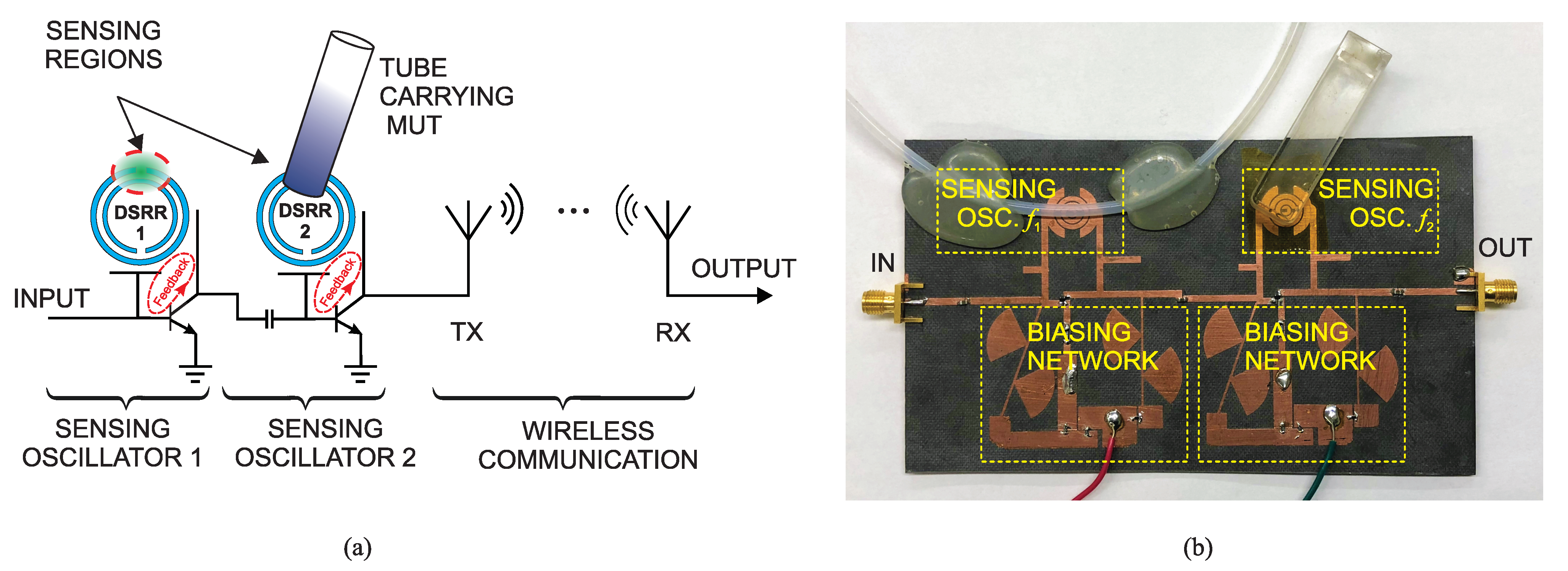
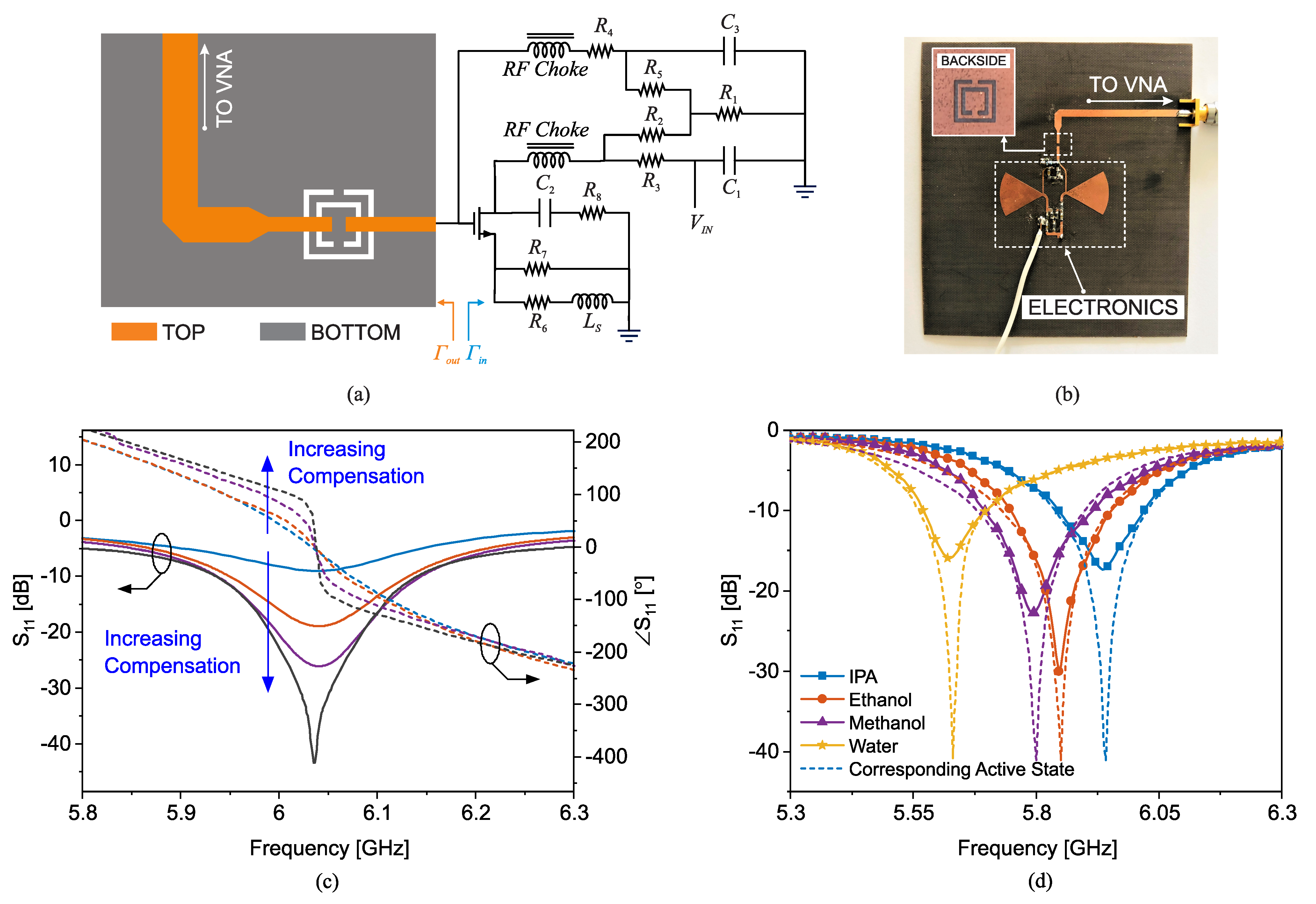
In this design, the second sensing oscillator is used as both generator of and the mixing element for the signal being injected from the first stage. The second stage needs to operate at a nonlinear region for the bandwidth of interest to allow for mixing products being produced with reasonable gain at the output. This mixer design is followed by a pair of wide-band high-gain linear antennas for transmission purposes. The use of an antenna illustrates that the proposed sensing technique can be integrated with peripheral electronic receivers to enable radio frequency identification (RFID).
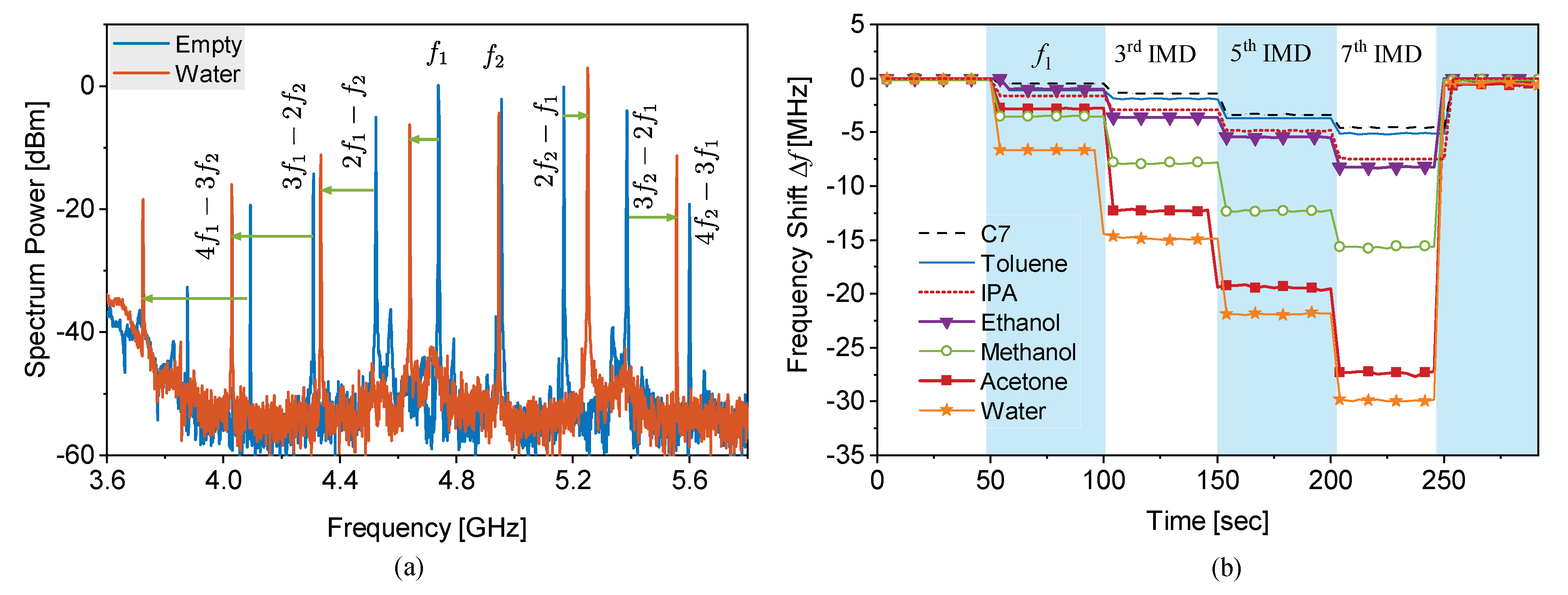
The experimental verification of the mixer sensor is conducted using a PTFE tubing
as a carrier, and is configured on the first stage with a lower oscillation frequency
to freely shift without interfering with
. The mixer sensor is fabricated on Rogers RO5880 substrate (see
Figure 38b) and is connected to a pair of wide-band slot bow-tie antennas. Once the antennas are separated by 30 cm, the received power at the receiving antenna is measured using a power meter. The sensor is examined with water as the external analyte to exhibit its fundamental functionality. Since the tube is directly affecting the first stage, the oscillation frequency
is downshifted. However, the second stage with
is located at a distance with respect to the first resonator, and then is left unaffected. IMPs with orders of 3, 5 and 7 have frequency differences of
,
and
from
, as well as reveal correspondingly increased downshifts. This represents that the proposed sensor allows for up to 3-fold sensitivity enhancement at a lower frequency, which simplifies the post-processing in commercial applications.
In another experiment, the sensitivity enhancement is compared between
, toluene, IPA, ethanol, methanol, acetone, and water, as shown in
Figure 39b. Assuming that
undergoes a certain change in the frequency, the higher-order IMPs represent multiplied shifts that are consistent for a wide range of permittivity ranging from single-digit
for
and toluene to a larger value for water.
A reasonable concern for such sensors is the possible accumulation of
,
phase noise and its appearance in the IMP with the same enhancement factor. In this regard, the authors in [
41] have well studied this issue and reported a possible and feasible case considering which such a disturbing factor is avoided in the sensor response. It has been shown that the phase lag between two incoming signals (currents) need to be infinitesimal, which is realized by shortening the distance between the output of the first stage and the input of the second stage.


