Author Contributions
Conceptualization, M.H. and P.K.; methodology, M.H.; software, P.K.; validation, M.L. and V.P.; formal analysis, P.K.; investigation, M.H.; resources, P.K.; data curation, V.P.; writing—original draft preparation, M.H.; writing—review and editing, P.K.; visualization, P.K.; supervision, M.L.; project administration, V.P.; funding acquisition, M.H. All authors have read and agreed to the published version of the manuscript.
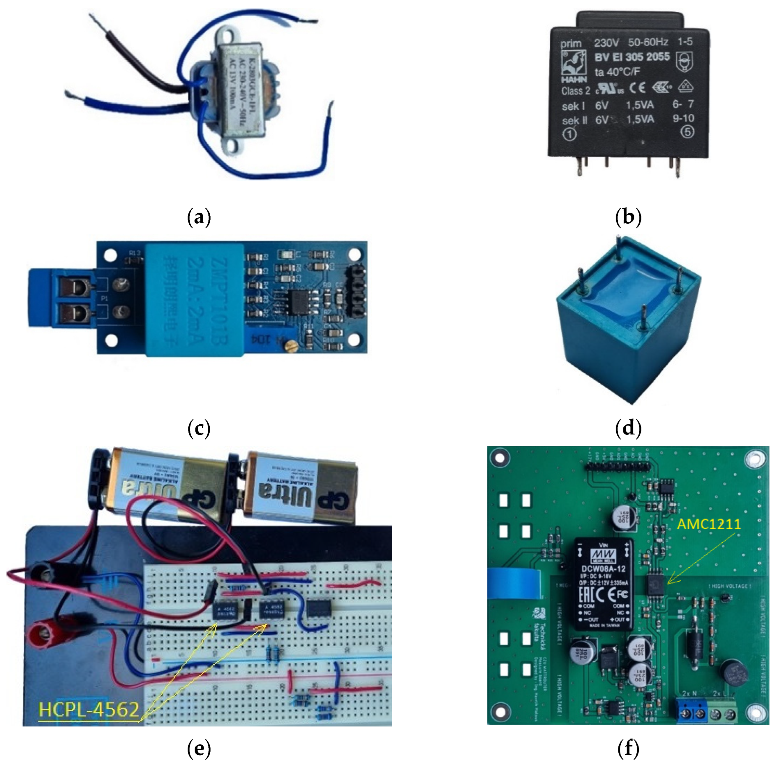
Figure 1.
(a) K-2803GCE-1FL transformer, (b) BV EI 305 2055 HAHN transformer, (c) ZMPT101B single-phase AC voltage sensor, (d) Stand-alone current transformer ZMPT101B, (e) The fixture with the optocouplers HCPL-4562, (f) The fixture with an AMC1211 circuit.
Figure 1.
(a) K-2803GCE-1FL transformer, (b) BV EI 305 2055 HAHN transformer, (c) ZMPT101B single-phase AC voltage sensor, (d) Stand-alone current transformer ZMPT101B, (e) The fixture with the optocouplers HCPL-4562, (f) The fixture with an AMC1211 circuit.
Figure 2.
Measuring circuit diagram with K-2803GCE-1FL transformer.
Figure 2.
Measuring circuit diagram with K-2803GCE-1FL transformer.
Figure 3.
Measuring circuit diagram with BV EI 305 2055 HAHN transformer.
Figure 3.
Measuring circuit diagram with BV EI 305 2055 HAHN transformer.
Figure 4.
The wiring of the ZMPT101B single-phase AC voltage sensor and its internal diagram.
Figure 4.
The wiring of the ZMPT101B single-phase AC voltage sensor and its internal diagram.
Figure 5.
The wiring diagram of the fixture with the stand-alone current transformer ZMPT101B.
Figure 5.
The wiring diagram of the fixture with the stand-alone current transformer ZMPT101B.
Figure 6.
The wiring of the fixture with the optocouplers HCPL-4562. HCPL-4562 circuit pins: 1-not connected, 2-LED anode, 3-LED cathode, 4-not connected, 5-transistor emitter, 6-transistor collector, 7-transistor base and photodiode anode, 8-photodiode cathode.
Figure 6.
The wiring of the fixture with the optocouplers HCPL-4562. HCPL-4562 circuit pins: 1-not connected, 2-LED anode, 3-LED cathode, 4-not connected, 5-transistor emitter, 6-transistor collector, 7-transistor base and photodiode anode, 8-photodiode cathode.
Figure 7.
The circuit diagram of the fixture with the resistive divider and the AMC1211 integrated circuit.
Figure 7.
The circuit diagram of the fixture with the resistive divider and the AMC1211 integrated circuit.
Figure 8.
The wiring diagram of the measuring apparatus. The Live (L) and Neutral (N) contacts of mains are connected to the primary winding of the isolation transformer. One of the outputs of the isolation transformer secondary winding is selected as a common floating ground for grounding the PC, A/D converter, high-voltage (HV) and low-voltage (LV) sides of the fixtures and resistive dividers. If the maximum output voltage from the fixture was higher than the range of the AD converter, the signal for CH1 was sensed at the voltage divider (R3, R4).
Figure 9.
(a) The input and output signal record of the K-2803GCE-1FL (black line—mains; grey line—output); (b) Normalized and zero-crossing time shift-corrected input and output waveforms of K-2803GCE-1FL transformer (black line—mains; grey line—output).
Figure 9.
(a) The input and output signal record of the K-2803GCE-1FL (black line—mains; grey line—output); (b) Normalized and zero-crossing time shift-corrected input and output waveforms of K-2803GCE-1FL transformer (black line—mains; grey line—output).
Figure 10.
(a) The input and output signal record of the BV EI 305 2055 transformer (black line–mains, grey line–output); (b) Normalized and zero-crossing time shift-corrected input and output waveforms BV EI 305 2055 transformer (black line—mains; grey line—output).
Figure 10.
(a) The input and output signal record of the BV EI 305 2055 transformer (black line–mains, grey line–output); (b) Normalized and zero-crossing time shift-corrected input and output waveforms BV EI 305 2055 transformer (black line—mains; grey line—output).
Figure 11.
(a) The input and output signal record of ZMPT101B single-phase AC voltage sensor (black line—mains; grey line—output); (b) Normalized and zero-crossing time shift-corrected input and output waveforms of ZMPT101B single-phase AC voltage sensor (black line—mains; grey line—output).
Figure 11.
(a) The input and output signal record of ZMPT101B single-phase AC voltage sensor (black line—mains; grey line—output); (b) Normalized and zero-crossing time shift-corrected input and output waveforms of ZMPT101B single-phase AC voltage sensor (black line—mains; grey line—output).
Figure 12.
(a) The input and output signal record of ZMPT101B current transformer (black line—mains; grey line—output); (b) Normalized and zero-crossing time shift-corrected input and output waveforms of ZMPT current transformer (black line—mains; grey line—output).
Figure 12.
(a) The input and output signal record of ZMPT101B current transformer (black line—mains; grey line—output); (b) Normalized and zero-crossing time shift-corrected input and output waveforms of ZMPT current transformer (black line—mains; grey line—output).
Figure 13.
(a) The input and output signal record of optocouplers HCPL-4562 (black line—mains; grey line—output); (b) Normalized input and output waveforms of optocouplers HCPL-4562 (black line—mains; grey line—output).
Figure 13.
(a) The input and output signal record of optocouplers HCPL-4562 (black line—mains; grey line—output); (b) Normalized input and output waveforms of optocouplers HCPL-4562 (black line—mains; grey line—output).
Figure 14.
The transfer characteristics of the input and output currents of two optocouplers HCPL-4562 (black lines—characteristics of both optocouplers; dotted lines—linear dependencies of input and output quantities given by corresponding end points of optocoupler characteristics).
Figure 14.
The transfer characteristics of the input and output currents of two optocouplers HCPL-4562 (black lines—characteristics of both optocouplers; dotted lines—linear dependencies of input and output quantities given by corresponding end points of optocoupler characteristics).
Figure 15.
(a) The input and output signal record of AMC1211 isolated amplifier (black line—mains; grey line—output); (b) Normalized input and output waveforms of AMC1211 isolated amplifier (black line—mains; grey line—output).
Figure 15.
(a) The input and output signal record of AMC1211 isolated amplifier (black line—mains; grey line—output); (b) Normalized input and output waveforms of AMC1211 isolated amplifier (black line—mains; grey line—output).
Figure 16.
(a) Differences in instantaneous values of normalized and time-corrected input and output signals of one period for transformer K-2803GCE-1FL (black line) and ZMPT101B single-phase AC voltage sensor (grey line); (b) Differences in instantaneous values of normalized and time-corrected input and output signals of one period for fixture with HCPL-4562 optocouplers. The sharp jump in the plotted values near the zero crossing of the input signal (0, 0.01, 0.02 s) is clearly visible.
Table 1.
Amplitudes of the first five odd harmonic components of the frequency spectrum of the waveforms normalized by the value of the amplitude of the first harmonic component.
Table 1.
Amplitudes of the first five odd harmonic components of the frequency spectrum of the waveforms normalized by the value of the amplitude of the first harmonic component.
| | | K-2803GCE-1FL | BV EI 305 2055 | ZMPT101B on PCB | ZMPT101B | HCPL-4562 | AMC1211 |
|---|
| Order | f(Hz) | Mains | Output | Mains | Output | Mains | Output | Mains | Output | Mains | Output | Mains | Output |
|---|
| 1 | 50 | 1.000 | 1.000 | 1.000 | 1.000 | 1.000 | 1.000 | 1.000 | 1.000 | 1.000 | 1.000 | 1.000 | 1.000 |
| 3 | 150 | 0.014 | 0.134 | 0.013 | 0.029 | 0.013 | 0.013 | 0.012 | 0.011 | 0.011 | 0.011 | 0.014 | 0.014 |
| 5 | 250 | 0.030 | 0.062 | 0.028 | 0.034 | 0.028 | 0.031 | 0.019 | 0.018 | 0.020 | 0.028 | 0.027 | 0.028 |
| 7 | 350 | 0.008 | 0.024 | 0.009 | 0.007 | 0.010 | 0.010 | 0.008 | 0.007 | 0.010 | 0.007 | 0.011 | 0.011 |
| 9 | 450 | 0.001 | 0.006 | 0.002 | 0.002 | 0.001 | 0.001 | 0.007 | 0.007 | 0.007 | 0.010 | 0.002 | 0.002 |
Table 2.
THDu of mains and output signal, increment of THDu, relative increase in THDu, and a phase shift in the first harmonic component of input and output waveforms.
Table 2.
THDu of mains and output signal, increment of THDu, relative increase in THDu, and a phase shift in the first harmonic component of input and output waveforms.
| | K-2803GCE-1FL | BV EI 305 2055 | ZMPT101B on PCB | ZMPT101B | HCPL-4562 | AMC1211 |
|---|
| THDu of mains [%] | 3.4 | 3.3 | 3.3 | 2.6 | 2.7 | 3.3 |
| THDu of fixture output [%] | 14.9 | 4.6 | 3.6 | 2.4 | 3.3 | 3.5 |
| increment of THDu [%] | 11.5 | 1.3 | 0.3 | −0.2 | 0.7 | 0.1 |
| relative increase in THDu [%] | 336.9 | 39.4 | 8.3 | −7.8 | 25.5 | 4.5 |
| phase shift in 1st harm. comp. [°] | −14.4 | −3.8 | −28.1 | −0.4 | −0.2 | 0.0 |
Table 3.
The phase shift in the signal zero crossing of the input and output signals.
Table 3.
The phase shift in the signal zero crossing of the input and output signals.
| | K-2803GCE-1FL | BV EI 305 2055 | ZMPT101B on PCB | ZMPT101B | HCPL-4562 | AMC1211 |
|---|
| phase shift in zero crossing [°] | −25.8 | −5.9 | −29.5 | −0.4 | 0.0 | 0.0 |
Table 4.
The difference area error values calculated according to Equation (6) for the normalized input and output waveforms with time-corrected source data are in the row labelled “difference area error”. The difference area error values for output waveforms for which noise or interference has been reduced by averaging according to Equation (7) are shown in the row labelled “with noise reduction”. (NC—not calculated).
| | K-2803GCE-1FL | BV EI 305 2055 | ZMPT101B on PCB | ZMPT101B | HCPL-4562 | AMC1211 |
|---|
| difference area error [%] | 21.534 | 4.061 | 8.331 | 1.329 | 1.885 | 1.659 |
| with noise reduction [%] | NC | NC | NC | 1.033 | 1.829 | 0.746 |
Table 5.
The active power error values calculated according to Equation (9) for the normalized input and output waveforms with time-corrected data.
Table 5.
The active power error values calculated according to Equation (9) for the normalized input and output waveforms with time-corrected data.
| | K-2803GCE-1FL | BV EI 305 2055 | ZMPT101B on PCB | ZMPT101B | HCPL-4562 | AMC1211 |
|---|
| active power error [%] | 11.200 | 0.544 | 11.288 | 1.461 | 1.598 | −0.209 |
Table 6.
Summary of the calculated errors and the energy consumption of the input parts of the circuits. Difference area error values in parentheses correspond to the output signal corrected by the floating average calculation according to Formula (7). The input power loss values in parentheses correspond to the maximum adjustable input current.
| | K-2803GCE-1FL | BV EI 305 2055 | ZMPT101B on PCB | ZMPT101B | HCPL-4562 | AMC1211 |
|---|
| relative increase in THDu [%] | 336.9 | 39.4 | 8.3 | −7.8 | 25.5 | 4.5 |
| difference area error, (NR) [%] | 21.534 | 4.061 | 8.331 | 1.329, (1.033) | 1.885, (1.829) | 1.659, (0.746) |
| active power error [%] | 11.2 | 0.544 | 11.288 | 1.461 | 1.598 | −0.209 |
| phase shift in zero crossing [°] | −25.8 | −5.9 | −29.5 | −0.4 | 0 | 0 |
| input-side power loss, (max) [W] | 2.56 | 1.07 | 0.07 | 0.35, (0.46) | 2.76, (2.76) | 0.1 |


