
Wafer Center Alignment System of Transfer Robot Based on Reduced Number of Sensors
Korea Institute of Industrial Technology, Ansan 426-171, Korea
Sensors 2022, 22(21), 8521; https://doi.org/10.3390/s22218521
Submission received: 18 September 2022
/
Revised: 31 October 2022
/
Accepted: 2 November 2022
/
Published: 5 November 2022
(This article belongs to the Section Fault Diagnosis & Sensors)
Abstract
:This brief presents a wafer alignment algorithm with reduced sensor number that obtains the relative distance of the wafer center and the robot hand. By ‘reduced number’, in spite of smaller number of sensors than the conventional method, we mean an improved method which achieves the similar results to pre-existing algorithms. Indeed, it can be designed with only three sensor data, less than four sensors of the conventional algorithm. Thus, some advantages of the proposed alignment algorithm include that it can be designed with low cost and less computing power. The proposed alignment algorithm is applied to a transfer robot for coater/developer system in semiconductor processing for verifying the performance of the method. The performance of the proposed method is validated by both simulation and experimental results.
1. Introduction
The alignment problem of wafer center is a significant and critical topic in semiconductor manufacturing processing because it affects coating performance, chemical edge bead removal (EBR), and the backside rinse steps for lithographic applications [1]. Its effect increases when the semiconductor process enters the era of deep submicron meter (below 20 nm), e.g., EUV process. In order to solve the alignment problem, there are several approaches [2,3,4,5,6,7,8,9,10,11,12,13,14]. The most typical device is wafer pre-alignment system (which is called pre-aligner) that consists of rotation mechanics and optical vision sensor [6]. Although it can accurately detect the position of geometric center and notch direction, the system requires a rotating mechanism in order to find the information of maximum eccentricity and the notch, and then the motion process causes a delay in the processing. Instead of the rotational mechanism, a method using the straight motion of the robot hand holding the wafer was studied in [15,16]. The method, called AWC (automatic wafer centering), uses several thru-beam sensors to calculate the center of the wafer from the distance across it. Although this method is widely used in vacuum robots, the method also requires additional motion to obtain sensing information. To solve this, the authors of [17] have proposed an automatic alignment system that can detect the wafer center without the rotating mechanism. It consists of robot hand for wafer transfer and four vision sensors to obtain the wafer position information. Thus, without the additional aligner, it can align the wafer center whenever the transfer robot has the wafer on robot hand.
In this paper, we mainly focus on the case where the number of the sensors is one less than the previous studies. For this, the proposed algorithm is designed with only three sensor data, less than four sensors of the conventional method. Thus, some advantages of the proposed alignment algorithm include that it can be designed with low cost and less computing power. For the constructive design of the proposed method, we suggest some assumptions and provide mathematical proofs under them. In order to verify the performance, it is finally applied to a transfer robot for coater/developer system in semiconductor process.
The paper is organized as follows: in Section 2, an algorithm for finding the wafer center is presented. For this, we introduce some assumptions and lemmas for theoretical support (see Section 2.1). Moreover, Section 2.2 provides an algorithm to avoid a wafer notch. In Section 3, the proposed algorithm is experimentally tested for the transfer robot of coater/developer system. Finally, Conclusions are found in Section 4.
Notation: Cartesian plane with the familiar x- and y-axes is considered. The vector from A to B is denoted by ; the point A is called its tail and the point B is called its head. Then, the set of all points in the place corresponds to the set of all vectors whose tails are at the origin O. For example, the point and we write the vector using square brackets where implies the matrix transpose [18]. In this paper, all points are represented as a vector with the origin O as tail.
2. Main Results
Here, a detection method of wafer center is discussed that can be designed with only three sensor data as mentioned in the previous section. As is well known in the literature, it is possible to derive the wafer center from the circumcenter of a triangle because the shape of the wafer is a circle and the three sensor information are known. However, it may not be possible to determine the exact center due to the notch on the edge of the wafer, as shown in Figure 1. To solve this problem, the proposed method is composed of two parts. The first part is to obtain the wafer center from three sensor data and the known wafer radius r. In the second part, with the movement of the robot hand as shown in Figure 2, we introduce an algorithm for avoiding the notch cope with abnormal cases.
Now we consider the case of three sensors, and then its configuration with the installed sensors is shown in Figure 3. It is supposed that the measurable sensor range d is known. Additionally, the angles of installed sensors , and with respect to the Y-axis are known distinct positive number and it is assumed that . In order to obtain the actual wafer center , we assume the followings.
Assumption 1.
The range d is less than the wafer diameter , i.e., . For the sensor number , the sensing range (bold blue line in Figure 3) is a connected compact set as follows:
Assumption 2.
The actual wafer center is limited as follows:
Assumption 3.
If for any , . Otherwise, .
Here, Assumption 1 and 2 are acceptable conditions for the sensors and the wafer location to detect the wafer edge. Assumption 3 is required in order to identify the wafer center (to be discussed).
2.1. Center Calculation Algorithm
In this section, we propose an algorithm to find wafer center from sensor values. As shown in Figure 3, it follows that three points for at which the wafer edge is detected by the sensors are given by
where ’s are measurable sensor values. The existence of is proved in the following lemma.
Lemma 1.
For any , there exists a point , such that for .
Proof.
Equation (1) can be represented by
Here, it follows from Assumption 1 that because . Now, let
where is a rotation matrix as follows:
It is easy to show that with satisfies the equation . Moreover, it can be shown that as follows:
- Since , it follows from Assumption 2 that . Then, we can obtain
- Next, we haveDefine . Then, andis a monotonically increasing function on ([19], [page 95]) because it follows from of Assumption 1 that its derivative with respect to satisfies thatThis implies that
Then, for any , with
is the point that satisfies the equation . The proof is complete since the matrix is invertible [18]. □
Now, from the Equation (1), we can obtain the following equation of the three circles with radius r (red dashed circles in Figure 3)
Then, it follows that we can obtain two intersections for each pair , , as follows:
Here, under Assumption 3, the existence of the intersections is proved in the following lemma.
Lemma 2.
Under Assumption 1 and 3, there exist two distinct intersections for each pair , , .
Proof.
It is easy to show that there are two distinct intersections between the two circles and if for . From Assumption 1, , and , we have
- If for any , it follows from and of Assumption 3 that
- Otherwise, it follows from and of Assumption 3 that
Therefore, the proof is complete. □
In fact, Assumption 3 required for the proof of Lemma 2 is only sufficient. Thus, failure of Assumption 3 does not mean that two intersection points do not exist. Next, the following lemma shows the relationship between the wafer center and the intersections.
Lemma 3.
The wafer center is located at one of the two intersections for each pair , , , i.e.,
for .
Proof.
This implies that
Therefore, by the Equations (6)–(8), the proof is complete. □
Finally, it follows from Lemma 3 that we obtain the center of wafer as follows:
where such that
2.2. Notch Detection Algorithm
As shown in Figure 3, the notch on the wafer edge is one of the major obstacles to obtaining the correct wafer center. To solve the problem, a strategy using rotational motion was proposed in [20]. Instead of the rotational motion, we propose an algorithm with a prismatic motion of Figure 2 to archive the wafer center even if the notch is placed on the sensor. The proposed algorithm proceeds sequentially as follows:
- Start
- From the algorithm of Section 2.1, find the intersections and let , , .
- If is less than , jump to 7.
- Move the robot hand holding the wafer by in the X-direction where is a positive number.
- Similar to 2, try again and define , , .
- Select as the center of wafer where j is chosen to minimize for and . Then, jump to 8.
- Select as the center of wafer.
- End.
Here, and are suitable design parameters. Because it is necessary to change the sensor value through the motion in the X-direction, it is also supposed that and for .
3. Experimental Results
Here, the proposed wafer alignment algorithm is implemented for an actual 300 mm coater/developer system in semiconductor processing for verifying the performance of the method as shown in Figure 4. For this, the thru-beam type digital displacement sensors and controllers (HG-T series manufactured by Panasonic Industry Company) are used in the experiment. To transmit the sensor data to the PC, RS-485 communication is used. The measurable sensor range is d = 5 mm and the angles of installed sensors are , and . It is noted that the parameter , and satisfies Assumption 3.
Figure 5 shows the experimental results of the proposed algorithm and the conventional algorithm of [17], respectively, in which, axis-x and axis-y imply the actual center coordinates of the wafer and the error between it and the calculated center using the proposed algorithm in the paper, respectively. As shown in Table 1, the peak-to-peak error in both algorithms is less than about 0.022 mm in the x and y directions, respectively (The upper bound of the specification is 0.2 mm).
As shown in Figure 6, through the pick and place operation, the robot transfers the wafer to the desired position. The X-axis is capable of high-precision motion with short strokes, while the Y-axis is the traverse direction that moves the robot body, and, thus, the motion precision of the Y-axis is relatively low. Therefore, although the required specifications are satisfied, the error in the Y-direction is larger than that in the X-direction.
To verify the ability of the notch detection algorithm proposed in Section 2.2, we carry out an experiment when the wafer notch is located on the sensor 3. The parameters for the notch algorithm chosen as
As shown in Figure 7a, the point is relatively far from and , i.e., . To solve the problem, by the notch detection algorithm, the wafer is moved by = 1 mm in the X-direction. Then, the point only moves in the X-direction, but the rest points also have the Y-direction movement, as shown in Figure 7b. Thus, we can select as the wafer center (see the notch detection algorithm in Section 2.2).
4. Conclusions
In this brief, a wafer alignment algorithm has been presented for obtaining the relative distance between the wafer center and the robot hand center. The proposed algorithm can have been designed with only three sensor data less than the conventional algorithm, and, therefore, it has achieved low cost and less computing power. It has been verified that its performance is similar to the conventional method through a actual robot system consisting of three thru-beam type digital displacement sensors.
Funding
This research was supported by the Korea Evaluation Institute Of Industrial Technology (Grant No: 20008905).
Institutional Review Board Statement
Not applicable.
Informed Consent Statement
Not applicable.
Data Availability Statement
Not applicable.
Conflicts of Interest
The authors declare no conflict of interest.
References
- Jekauc, I.; Watt, M.; Hornsmith, T.; Tiffany, J. Necessity of chemical edge bead removal in modern day lithographic processing. In Proceedings of the Advances in Resist Technology and Processing XXI; Sturtevant, J.L., Ed.; International Society for Optics and Photonics, SPIE: Bellingham, WA, USA, 2004; Volume 5376, pp. 1255–1263. [Google Scholar] [CrossRef]
- Tadashi, H. Method of Detecting Position of Orientation Flat of Semiconductor Wafer. JP Patent 06236918, 23 August 1994. [Google Scholar]
- Berken, L.M. Wafer Positioning System. U.S. Patent 5740062, 14 April 1998. [Google Scholar]
- Freerks, F.W. Wafer Position Error Detection and Correction System. U.S. Patent 5980194, 9 November 1999. [Google Scholar]
- Yoo, W.S. Wafer Alignment System and Method. U.S. Patent 6516244, 4 February 2003. [Google Scholar]
- Cong, M.; Kong, X.; Du, Y.; Liu, J. Wafer Pre-Aligner System Based on Vision Information Processing. Inf. Technol. J. 2007, 6, 1245–1251. [Google Scholar] [CrossRef] [Green Version]
- Qu, D.; Qiao, S.; Rong, W.; Song, Y.; Zhao, Y. Design and Experiment of The Wafer Pre-alignment System. In Proceedings of the 2007 International Conference on Mechatronics and Automation, Harbin, China, 5–8 August 2007; pp. 1483–1488. [Google Scholar]
- Chen, Y.; Chen, Y.; Lee, J. A novel method for real-time wafer positioning during transfer process. In Proceedings of the SICE Annual Conference 2011, Tokyo, Japan, 13–18 September 2011; pp. 1933–1937. [Google Scholar]
- Chen, Y.; Lee, Y.; Lee, J.; Chen, J. Implementation of a wafer positioning system. In Proceedings of the SICE Annual Conference 2011, Tokyo, Japan, 13–18 September 2011; pp. 1938–1943. [Google Scholar]
- Chen, Y.; Chen, Y.; Lee, J. Experimental results of a wafer positioning system using machine vision after system calibration. In Proceedings of the 2012 Proceedings of SICE Annual Conference (SICE), Akita, Japan, 20–23 August 2012; pp. 1014–1017. [Google Scholar]
- He, Y.; Zhang, C.; Ye, W.; He, Z.; Chen, X.; Gao, J.; Zhang, K.; Yang, Z.; Chen, X.; Chen, Y.; et al. A direct-drive SCARA robot for wafer ceramic-substrate handling based on visual servoing. In Proceedings of the 2017 IEEE International Conference on Cybernetics and Intelligent Systems (CIS) and IEEE Conference on Robotics, Automation and Mechatronics (RAM), Ningbo, China, 19–21 November 2017; pp. 428–433. [Google Scholar]
- Xu, J.; Hu, H.; Lei, Y.; Liu, H. A Wafer Prealignment Algorithm Based on Fourier Transform and Least Square Regression. IEEE Trans. Autom. Sci. Eng. 2017, 14, 1771–1777. [Google Scholar] [CrossRef]
- Kim, J. New Wafer Alignment Process Using Multiple Vision Method for Industrial Manufacturing. Electronics 2018, 7, 39. [Google Scholar] [CrossRef] [Green Version]
- Pan, S.; Wang, S.; Xu, J.; Fan, L.; Yuan, F.; Shu, T.; Dai, F.; Yan, X.; Bu, Y.; Wang, X. Sub-pixel position estimation algorithm based on Gaussian fitting and sampling theorem interpolation for wafer alignment. Appl. Opt. 2021, 60, 9607–9618. [Google Scholar] [CrossRef] [PubMed]
- Chung, M.J.; Lee, S.J. Development of Automatic Wafer Centering System for Vacuum Transfer Robot using for Semiconductor Manufacturing. Appl. Mech. Mater. 2014, 607, 782–785. [Google Scholar] [CrossRef]
- Cheng, H.; Chen, S.; Mooring, B.W. Accuracy Analysis of Dynamic-Wafer-Handling Robotic System in Semiconductor Manufacturing. IEEE Trans. Ind. Electron. 2014, 61, 1402–1410. [Google Scholar] [CrossRef]
- Hayashi, T. Substrate Transfer Apparatus, Substrate Transfer Method, and Recording Medium Having Recorded Program for Executing the Substrate Transfer Method. U.S. Patent 1017908670000, 16 March 2016. [Google Scholar]
- Poole, D. Linear Algebra: A Modern Introduction; Available Titles CengageNOW Series; Thomson Brooks/Cole: Pacific Grove, CA, USA, 2005. [Google Scholar]
- Rudin, W. Principles of Mathematical Analysis; International Series in Pure and Applied Mathematics; McGraw-Hill: New York, NY, USA, 1976. [Google Scholar]
- Yamamoto, S.; Kamei, K. Apparatus for Detecting Position of a Notch in a Semiconductor Wafer. U.S. Patent US5438209A, 1 August 1995. [Google Scholar]
Figure 1.
Wafer center alignment system with four sensors.
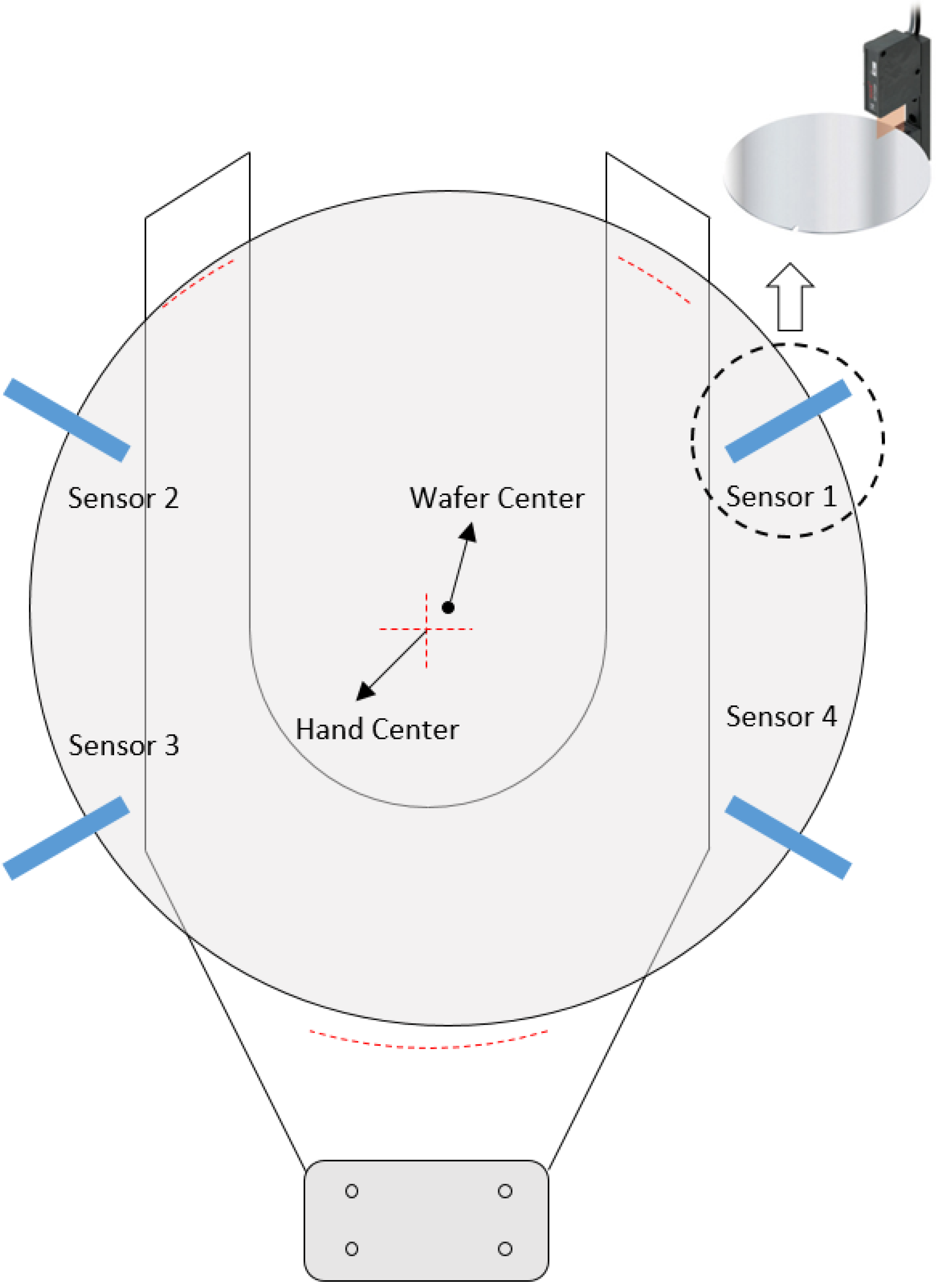
Figure 2.
Motion of robot hand holding the wafer (with four sensors).

Figure 3.
Configuration of alignment system with three sensors.

Figure 4.
Experimental setup.

Figure 5.
Experimental results of the proposed algorithm (left) and the conventional algorithm (right).
Figure 5.
Experimental results of the proposed algorithm (left) and the conventional algorithm (right).

Figure 6.
Wafer pick and place for experiments.

Figure 7.
Experimental results of notch case (a) and after 1 mm motion in the X-direction (b).


Table 1.
Peak-to-peak error for the 20 times repeated test (unit: mm).
| Wafer Center X, Y | Proposed | Conventional | ||
|---|---|---|---|---|
| X-Dir | Y-Dir | X-Dir | Y-Dir | |
| (0,0) | 0.0145 | 0.0087 | 0.0153 | 0.0083 |
| (1.8,0) | 0.0143 | 0.0068 | 0.0213 | 0.0059 |
| (0.9,0.8) | 0.0144 | 0.0067 | 0.0125 | 0.0071 |
| (0,1.6) | 0.0116 | 0.0047 | 0.0157 | 0.0072 |
| (−0.9,0.8) | 0.0119 | 0.0076 | 0.0141 | 0.0072 |
| (−1.8,0) | 0.0215 | 0.0071 | 0.0202 | 0.0066 |
| (−0.9,−0.8) | 0.0122 | 0.0051 | 0.0106 | 0.0052 |
| (0,−1.6) | 0.0088 | 0.0067 | 0.0089 | 0.0062 |
| (0.9,−0.8) | 0.0162 | 0.0070 | 0.0177 | 0.0068 |
Publisher’s Note: MDPI stays neutral with regard to jurisdictional claims in published maps and institutional affiliations. |
© 2022 by the author. Licensee MDPI, Basel, Switzerland. This article is an open access article distributed under the terms and conditions of the Creative Commons Attribution (CC BY) license (https://creativecommons.org/licenses/by/4.0/).
Share and Cite
MDPI and ACS Style
Kim, H. Wafer Center Alignment System of Transfer Robot Based on Reduced Number of Sensors. Sensors 2022, 22, 8521. https://doi.org/10.3390/s22218521
AMA Style
Kim H. Wafer Center Alignment System of Transfer Robot Based on Reduced Number of Sensors. Sensors. 2022; 22(21):8521. https://doi.org/10.3390/s22218521
Chicago/Turabian StyleKim, Hyungjong. 2022. "Wafer Center Alignment System of Transfer Robot Based on Reduced Number of Sensors" Sensors 22, no. 21: 8521. https://doi.org/10.3390/s22218521
Note that from the first issue of 2016, this journal uses article numbers instead of page numbers. See further details here.