
Optimization of Silicon Nitride Waveguide Platform for On-Chip Virus Detection


Abstract
:1. Introduction
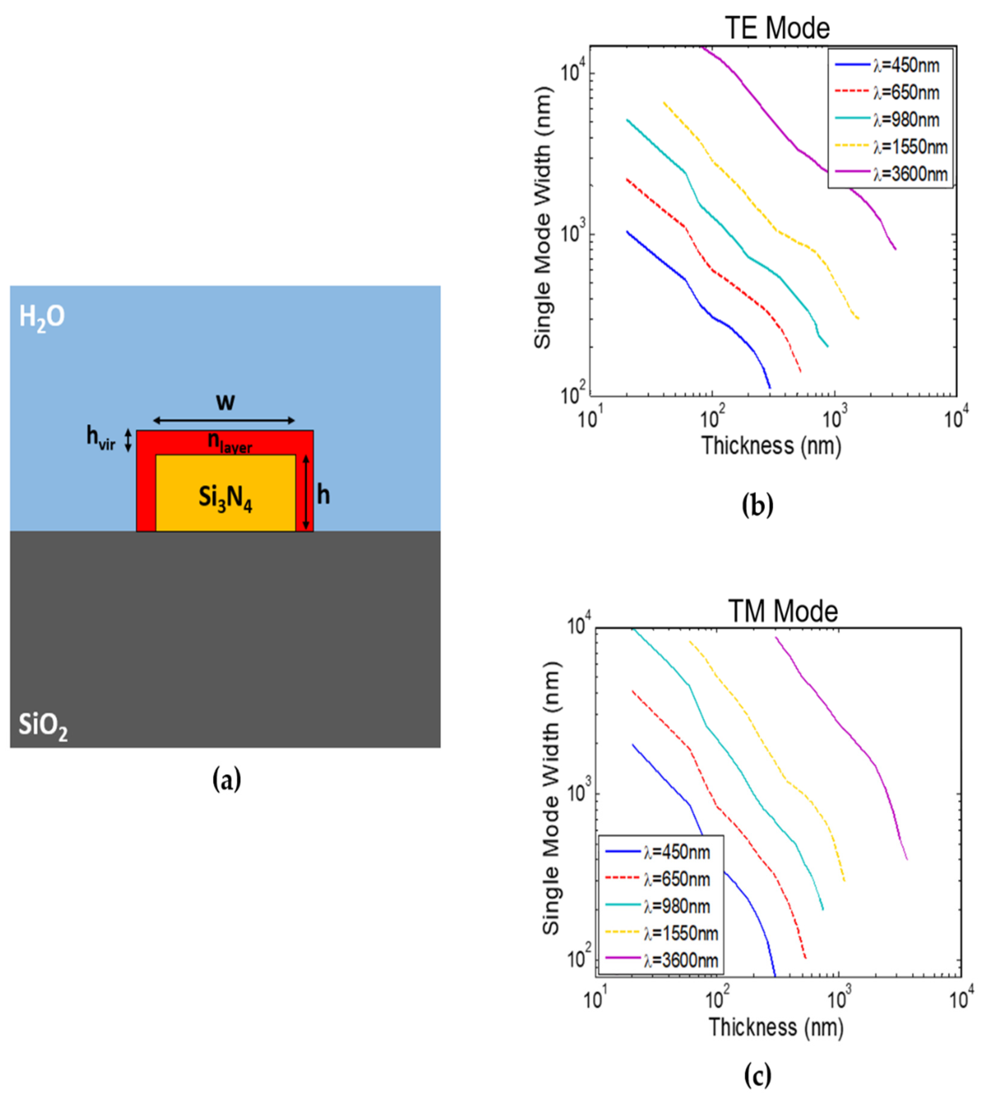
2. Virus Sensing Waveguide Analysis and Discussion
3. Virus Sensors Design
4. Edge Fiber Coupling of Designed Sensors
5. Conclusions
Author Contributions
Funding
Data Availability Statement
Conflicts of Interest
References
- WHO. The Top 10 Causes of Death. WHO 2017. Available online: http://www.who.int/mediacentre/factsheets/fs310/en/ (accessed on 30 December 2021).
- Piatak, M., Jr.; Saag, M.S.; Yang, L.C.; Clark, S.J.; Kappes, J.C.; Luk, K.C.; Hahn, B.H.; Shaw, G.M.; Lifson, J.D. High levels of HIV-1 in plasma during all stages of infection determined by competitive PCR. Science 1993, 259, 1749–1754. [Google Scholar] [CrossRef] [PubMed] [Green Version]
- Bastos, A.R.; Vicente, C.; Oliveira-Silva, R.; Silva, N.J.; Tacão, M.; Costa, J.P.d.; Lima, M.; André, P.S.; Ferreira, R.A. Integrated optical Mach-Zehnder interferometer based on organic-inorganic hybrids for photonics-on-a-chip biosensing applications. Sensors 2018, 18, 840. [Google Scholar] [CrossRef] [PubMed] [Green Version]
- Murib, M.S.; Martens, D.; Bienstman, P. Label-free real-time optical monitoring of DNA hybridization using SiN Mach–Zehnder interferometer-based integrated biosensing platform. J. Biomed. Opt. 2018, 23, 127002. [Google Scholar] [CrossRef] [PubMed]
- Liu, Q.; Tu, X.; Kim, K.W.; Kee, J.S.; Shin, Y.; Han, K.; Yoon, Y.-J.; Lo, G.-Q.; Park, M.K. Highly sensitive Mach–Zehnder interferometer biosensor based on silicon nitride slot waveguide. Sens. Actuators B Chem. 2013, 188, 681–688. [Google Scholar] [CrossRef]
- Bryan, M.R.; Steiner, D.J.; Cognetti, J.S.; Miller, B.L. Design, manufacture, and testing of a silicon nitride ring resonator-based biosensing platform. In Chemical 2018, Biological, Radiological, Nuclear, and Explosives (CBRNE) Sensing XIX; International Society for Optics and Photonics: Bellingham, WA, USA, 2018; Volume 10629, p. 106290Z. [Google Scholar]
- Besselink, G.A.; Geuzebroek, D.H.; Schreuder, F.; Falke, F.; Leinse, A.; Heideman, R.G. Microring resonator biosensing platform for sensitive detection of thrombin. In Microfluidics 2019, BioMEMS, and Medical Microsystems XVII; International Society for Optics and Photonics: Bellingham, WA, USA, 2019; Volume 10875, p. 1087511. [Google Scholar]
- Al Mahmod, M.J.; Hyder, R.; Islam, M.Z. A highly sensitive metal–insulator–metal ring resonator-based nanophotonic structure for biosensing applications. IEEE Sens. J. 2018, 18, 6563–6568. [Google Scholar] [CrossRef]
- Wang, X.; Flueckiger, J.; Schmidt, S.; Grist, S.; Fard, S.T.; Kirk, J.; Doerfler, M.; Cheung, K.C.; Ratner, D.M.; Chrostowski, L. A silicon photonic biosensor using phase-shifted Bragg gratings in slot waveguide. J. Biophotonics 2013, 6, 821–828. [Google Scholar] [CrossRef]
- Sakamoto, H.; Minpou, Y.; Sawai, T.; Enami, Y.; Suye, S.-i. A novel optical biosensing system using Mach–Zehnder-type optical waveguide for influenza virus detection. Appl. Biochem. Biotechnol. 2016, 178, 687–694. [Google Scholar] [CrossRef]
- Ymeti, A.; Greve, J.; Lambeck, P.V.; Wink, T.; van Hövell, S.W.; Beumer, T.A.; Wijn, R.R.; Heideman, R.G.; Subramaniam, V.; Kanger, J.S. Fast, ultrasensitive virus detection using a young interferometer sensor. Nano Lett. 2007, 7, 394–397. [Google Scholar] [CrossRef]
- Porcel, M.A.; Hinojosa, A.; Jans, H.; Stassen, A.; Goyvaerts, J.; Geuzebroek, D.; Geiselmann, M.; Dominguez, C.; Artundo, I. Silicon nitride photonic integration for visible light applications. Opt. Laser Technol. 2019, 112, 299–306. [Google Scholar] [CrossRef]
- Wilmart, Q.; El Dirani, H.; Tyler, N.; Fowler, D.; Malhouitre, S.; Garcia, S.; Casale, M.; Kerdiles, S.; Hassan, K.; Monat, C. A versatile silicon-silicon nitride photonics platform for enhanced functionalities and applications. Appl. Sci. 2019, 9, 255. [Google Scholar] [CrossRef] [Green Version]
- Baets, R.; Subramanian, A.Z.; Clemmen, S.; Kuyken, B.; Bienstman, P.; Le Thomas, N.; Roelkens, G.; Van Thourhout, D.; Helin, P.; Severi, S. Silicon Photonics: Silicon nitride versus silicon-on-insulator. In Optical Fiber Communication Conference; Optical Society of America: Washington, DC, USA, 2016; p. Th3J-1. [Google Scholar]
- Sharma, T.; Wang, J.; Kaushik, B.K.; Cheng, Z.; Kumar, R.; Zhao, W.; Li, X. Review of recent progress on silicon nitride-based photonic integrated circuits. IEEE Access 2020, 8, 195436–195446. [Google Scholar] [CrossRef]
- Poulton, C.V.; Byrd, M.J.; Raval, M.; Su, Z.; Li, N.; Timurdogan, E.; Coolbaugh, D.; Vermeulen, D.; Watts, M.R. Large-scale silicon nitride nanophotonic phased arrays at infrared and visible wavelengths. Opt. Lett. 2017, 42, 21–24. [Google Scholar] [CrossRef] [PubMed]
- Miller, S.; Luke, K.; Okawachi, Y.; Cardenas, J.; Gaeta, A.L.; Lipson, M. On-chip frequency comb generation at visible wavelengths via simultaneous second-and third-order optical nonlinearities. Opt. Express 2014, 22, 26517–26525. [Google Scholar] [CrossRef] [PubMed]
- Zhao, H.; Kuyken, B.; Clemmen, S.; Leo, F.; Subramanian, A.; Dhakal, A.; Helin, P.; Severi, S.; Brainis, E.; Roelkens, G. Visible-to-near-infrared octave spanning supercontinuum generation in a silicon nitride waveguide. Opt. Lett. 2015, 40, 2177–2180. [Google Scholar] [CrossRef] [PubMed] [Green Version]
- Xuan, Y.; Liu, Y.; Varghese, L.T.; Metcalf, A.J.; Xue, X.; Wang, P.-H.; Han, K.; Jaramillo-Villegas, J.A.; Al Noman, A.; Wang, C. High-Q silicon nitride microresonators exhibiting low-power frequency comb initiation. Optica 2016, 3, 1171–1180. [Google Scholar] [CrossRef] [Green Version]
- Optical Waveguide Design Software-Lumerical MODE Solutions Lumerical. Available online: https://www.lumerical.com/products/mode-solutions/ (accessed on 20 December 2021).
- Tavazzi, G.; Pellegrini, C.; Maurelli, M.; Belliato, M.; Sciutti, F.; Bottazzi, A.; Sepe, P.A.; Resasco, T.; Camporotondo, R.; Bruno, R. Myocardial localization of coronavirus in COVID-19 cardiogenic shock. Eur. J. Heart Fail. 2020, 22, 911–915. [Google Scholar] [CrossRef] [PubMed] [Green Version]
- Sahin, A.-R.; Erdogan, A.; Agaoglu, P.M.; Dineri, Y.; Cakirci, A.-Y.; Senel, M.-E.; Okyay, R.-A.; Tasdogan, A.-M. 2019 novel coronavirus (COVID-19) outbreak: A review of the current literature. EJMO 2020, 4, 1–7. [Google Scholar] [CrossRef]
- Philipp, H.R. Optical properties of silicon nitride. J. Electrochem. Soc. 1973, 120, 295. [Google Scholar] [CrossRef]
- Palik, E.D. Handbook of Optical Constants of Solids; Academic Press: Cambridge, MA, USA, 1998; Volume 3. [Google Scholar]
- Shi, Y.; Ma, K.; Dai, D. Sensitivity enhancement in Si nanophotonic waveguides used for refractive index sensing. Sensors 2016, 16, 324. [Google Scholar] [CrossRef] [Green Version]
- Barrios, C.A.; Banuls, M.J.; Gonzalez-Pedro, V.; Gylfason, K.B.; Sanchez, B.; Griol, A.; Maquieira, A.; Sohlström, H.; Holgado, M.; Casquel, R. Label-free optical biosensing with slot-waveguides. Opt. Lett. 2008, 33, 708–710. [Google Scholar] [CrossRef] [Green Version]
- El Shamy, R.S.; Swillam, M.A.; Khalil, D.A. Mid infrared integrated MZI gas sensor using suspended silicon waveguide. J. Lightwave Technol. 2019, 37, 4394–4400. [Google Scholar] [CrossRef]
- PIC Design and Simulation Software-Lumerical Interconnect Lumerical. Available online: https://www.lumerical.com/products/interconnect/ (accessed on 20 December 2021).
- Luan, E.; Shoman, H.; Ratner, D.M.; Cheung, K.C.; Chrostowski, L. Silicon photonic biosensors using label-free detection. Sensors 2018, 18, 3519. [Google Scholar] [CrossRef] [PubMed] [Green Version]
- Luke, K.; Dutt, A.; Poitras, C.B.; Lipson, M. Overcoming Si3N4 film stress limitations for high quality factor ring resonators. Opt. Express 2013, 21, 22829–22833. [Google Scholar] [CrossRef] [PubMed] [Green Version]
- Krückel, C.J.; Fülöp, A.; Klintberg, T.; Bengtsson, J.; Andrekson, P.A. Linear and nonlinear characterization of low-stress high-confinement silicon-rich nitride waveguides. Opt. Express 2015, 23, 25827–25837. [Google Scholar] [CrossRef] [PubMed]
- Subramanian, A.; Neutens, P.; Dhakal, A.; Jansen, R.; Claes, T.; Rottenberg, X.; Peyskens, F.; Selvaraja, S.; Helin, P.; Du Bois, B. Low-loss singlemode PECVD silicon nitride photonic wire waveguides for 532–900 nm wavelength window fabricated within a CMOS pilot line. IEEE Photonics J. 2013, 5, 2202809. [Google Scholar] [CrossRef] [Green Version]
- El-Rayany, M.M.; El Shamy, R.S.; Swillam, M.A. A compact silicon-on-insulator gas sensor. In Silicon Photonics XIV; International Society for Optics and Photonics: Bellingham, WA, USA, 2019; Volume 10923, p. 109231M. [Google Scholar]
- Hong, J.; Spring, A.M.; Qiu, F.; Yokoyama, S. A high efficiency silicon nitride waveguide grating coupler with a multilayer bottom reflector. Sci. Rep. 2019, 9, 12988. [Google Scholar] [CrossRef] [PubMed]
- Mak, J.C.; Sacher, W.D.; Ying, H.; Luo, X.; Lo, P.G.-Q.; Poon, J.K. Multi-layer silicon nitride-on-silicon polarization-independent grating couplers. Opt. Express 2018, 26, 30623–30633. [Google Scholar] [CrossRef]
- Chen, Y.; Halir, R.; Molina-Fernández, Í.; Cheben, P.; He, J.-J. High-efficiency apodized-imaging chip-fiber grating coupler for silicon nitride waveguides. Opt. Lett. 2016, 41, 5059–5062. [Google Scholar] [CrossRef]
- Romero-García, S.; Merget, F.; Zhong, F.; Finkelstein, H.; Witzens, J. Silicon nitride CMOS-compatible platform for integrated photonics applications at visible wavelengths. Opt. Express 2013, 21, 14036–14046. [Google Scholar] [CrossRef]
- Song, J.H.; Kongnyuy, T.D.; Troia, B.; Saseendran, S.S.; Soussan, P.; Jansen, R.; Rottenberg, X. Grating devices on a silicon nitride technology platform for visible light applications. OSA Contin. 2019, 2, 1155–1165. [Google Scholar] [CrossRef]
- Sacher, W.D.; Luo, X.; Yang, Y.; Chen, F.-D.; Lordello, T.; Mak, J.C.C.; Liu, X.; Hu, T.; Xue, T.; Guo-Qiang Lo, P.; et al. Visible-light silicon nitride waveguide devices and implantable neurophotonic probes on thinned 200 mm silicon wafers. Opt. Express 2019, 27, 37400–37418. [Google Scholar] [CrossRef] [PubMed] [Green Version]
- Thorlabs a Global Manufacturer of Photonic Tools—THORLABS. Available online: https://www.thorlabs.com/newgrouppage9.cfm?objectgroup_id=949 (accessed on 30 December 2021).


| λ (nm) | AR | Dimensions (nm) | FOM (RIU−1) |
|---|---|---|---|
| 450 | 0.13 * | wsens = 550, wref = 520 and h = 70 | 501 |
| 0.37 * | wsens = 270, wref = 300 and h = 100 | 553 | |
| 1 | wsens = 138, wref = 145 and h = 140 | 812 | |
| 2.88 | wsens = 104, wref = 104 and h = 300 | 1231 | |
| 650 | 1.1 | wsens = 203, wref = 230 and h = 220 | 454 |
| 980 | 1.2 | wsens = 300, wref = 360 and h = 360 | 244 |
| 1550 | 1 | wsens = 512, wref = 850 and h = 500 | 100 |
| λ (nm) | Dimensions (nm) | FOM (RIU−1) |
|---|---|---|
| 650 | wsens = 1500, wref = 1000 and h = 80 | 158 |
| 980 | wsens = 1500, wref = 1100 and h = 160 | 127 |
| λ (nm) | AR | Δnmin | rmin (%) |
|---|---|---|---|
| 450 | 0.13 * | 2.0 × 10⁻³ | 1.29 |
| 0.37 * | 1.8 × 10⁻³ | 1.16 | |
| 1 | 1.2 × 10⁻³ | 0.79 | |
| 2.88 | 8.1 × 10⁻⁴ | 0.52 | |
| 650 | 0.05 * | 6.3 × 10⁻³ | 3.73 |
| S (nm/RIU) | FOM (RIU−1) | ||
|---|---|---|---|
| s-MZI | 3098 | 553 | |
| a-MZI | ΔL = 30 µm | 1316 | 540 |
| ΔL = 5 µm | 5579 | 530 | |
| LT-MZI | 3098 | 1106 | |
| λ (nm) | Waveguide (nm) | Technique | Coupling Loss (dB) | |
|---|---|---|---|---|
| [37] | 660 | 700 × 100 | Grating | 4.2 (M) |
| [38] | 532 | 350 × 180 | Grating | 6 (S) |
| 640 | 340 × 220 | Grating | 6.6 (S) 7.5 (M) | |
| [39] | 430–648 | 340 × 135 | Edge | 8–8.9 (M) |
| Our Designs | 450 | 550 × 70 | Edge with h step | 4.1 (S) |
| 270 × 100 | Edge with h step | 5.1 (S) | ||
| 650 | 1500 × 80 | Edge with h step | 2.47 (S) |
Publisher’s Note: MDPI stays neutral with regard to jurisdictional claims in published maps and institutional affiliations. |
© 2022 by the authors. Licensee MDPI, Basel, Switzerland. This article is an open access article distributed under the terms and conditions of the Creative Commons Attribution (CC BY) license (https://creativecommons.org/licenses/by/4.0/).
Share and Cite
El Shamy, R.S.; Swillam, M.A.; Li, X. Optimization of Silicon Nitride Waveguide Platform for On-Chip Virus Detection. Sensors 2022, 22, 1152. https://doi.org/10.3390/s22031152
El Shamy RS, Swillam MA, Li X. Optimization of Silicon Nitride Waveguide Platform for On-Chip Virus Detection. Sensors. 2022; 22(3):1152. https://doi.org/10.3390/s22031152
Chicago/Turabian StyleEl Shamy, Raghi S., Mohamed A. Swillam, and Xun Li. 2022. "Optimization of Silicon Nitride Waveguide Platform for On-Chip Virus Detection" Sensors 22, no. 3: 1152. https://doi.org/10.3390/s22031152