Abstract
This paper proposes a wide dynamic range (DR) and high-resolution discrete-time (DT) 2-order 4-bit sigma-delta modulator with a novel dynamic-modulated scaling-down (DM-SD) technology for non-invasive electroencephalogram (EEG) acquisition. The DM-SD technology can expand the input dynamic range and suppress large input offsets at the same time. The modulator was designed with 180nm CMOS technology with an area of 0.49 mm. We achieve a 118.1 dB SNDR when the input signal is 437.5 Hz and the signal bandwidth is 1500 Hz. Due to the proposed DM-SD technology, the DR is expanded to 126 dB. The power consumption of the whole modulator is 1.6 mW and a 177.8 dB Schreier figure-of-merit (FoMs) is realized.
1. Introduction
EEG is a kind of bioelectrical signal corresponding to the brain’s electrical activities. It can reflect whether the physiological activity of the human body is normal. Compared to the traditional diagnostic methods such as X-ray, the non-invasive EEG signal acquisition has the characteristics of no radiation and being non-invasive. As a result, it is widely used in neuroscience research, disease diagnosis, and treatment [1,2,3]. The capture of high-fidelity EEG signals is urgently demanded in brain-controlled applications, such as brain–computer interface (BCI) systems. Since the EEG signal is the weakest bioelectrical signal with extremely low amplitude (1–100 V), the acquisition system should achieve a high signal-to-noise ratio (SNR) in the analog front end [4,5]. As mentioned in [6], the EEG spikes have a bandwidth of 0.5 Hz–1 kHz, and this requires that the AFE has a kilohertz bandwidth. Moreover, EEG signal is easily affected by undesired interference and noise, such as power line interference, motion artifacts, and offset. So the signal acquisition circuit must have a wide dynamic range (DR) to avoid the circuit entering into saturation [7]. In addition, most EEG signal acquisition systems will use multi-channel acquisition to improve the spatial resolution, low power consumption should also be considered when designing the acquisition circuit.
Many high-performance ADCs for EEG signal acquisition have been proposed to solve the problems mentioned above in the past few years. Among them, the Nyquist-rate successive-approximation-register (SAR) ADC is widely used for EEG signal acquisition due to its high power efficiency and small area. In [8], an SAR ADC using a dynamic random storage unit for biological signal acquisition has been proposed, which achieves 9.26 bits at 26.24uW power consumption. However, the problems caused by capacitance mismatch limit the accuracy of SAR ADC. In the literature [9,10,11,12], various capacitance mismatch cancellation techniques have been used to reduce the impact. However, even with the most advanced calibration techniques, the ENOB of the SAR ADC proposed in these papers is limited to 16 bits due to the limitation of the noise inside the comparator. For higher resolution, the sigma-delta ADC is another option. Due to the use of oversampling technology, the sigma-delta ADC can obtain a higher SNDR. In [13], a 3-order 1-bit continuous-time modulator is proposed. The high-order modulator can cause stability problems and limit the DR of the modulator. Thus, the modulator’s DR only achieves 80 dB. In [14], a 5-bit quantifier continuous-time modulator is proposed to reduce the signal amplitude in the loop and improve the stability of the modulator. However, the continuous-time modulator is susceptible to process, voltage, and temperature (PVT) variation. The proposed modulator achieves a DR of 92.3 dB at 100 Hz bandwidth. In [15], A 3-order DT SDM is proposed. By introducing a resistor, the harmonic is suppressed and a 102.3 dB DR is achieved. However, the structure of the modulator and the setup accuracy of the integrators limit the dynamic range of the modulator. In summary, it is challenging to design an ADC with a wide DR and high resolution while consuming several milliwatts.
To solve the difficulties mentioned above, this paper proposes a DT sigma-delta modulator used for EEG acquisition. We propose the following technologies to improve the performance of the modulator. Firstly, we propose an innovative dynamic-modulated scaling-down (DM-SD) technology to extend the DR of the modulator. A scaling factor of 3/4 is introduced to avoid the modulator entering in saturation or instability state with a full-scale input. Secondly, a low parasitic capacitance integrator by introducing a “negative capacitance” has been proposed to reduce the setting error of the integrators induced by the parasitic capacitance. Thirdly, we propose a simple random circuit and use the randomized data weighted averaging (RnDWA) to reduce the mismatch of the feedback digital-to-analog converter (DAC). Finally, we use the voltage domain technology (VDT) to reduce the power consumption of the quantizer and analysis it in theory. With VDT, the power consumption of the quantizer and logic circuit can reduce by about 30%. The proposed modulator is implemented in 0.18 um CMOS technology with a power supply voltage of 5 V and 1.8 V, occupying an area of 0.49 mm. The simulation results show that when the input signal is 437.5 Hz with a 1500 Hz signal bandwidth, the proposed modulator can achieve 118.1 dB SNDR. Due to the proposed DM-SD technology, the DR of the modulator has been extended from 120 dB to 126 dB. The total power consumption of the modulator is 1.6 mW, corresponding to 177.8 dB FoMs.
2. System Design
2.1. Overview of System Architecture
The proposed DT modulator is shown in Figure 1. It is a 2-order 4-bit modulator with a 1500 Hz signal bandwidth and is driven by a 1.024 Mhz clock. The modulator consists of the proposed DM-SD module, the low parasitic capacitance integrators, and a 4-bit quantizer. The coefficients of the modulator have been carefully optimized to reduce the output swing of the integrator and save power consumption.
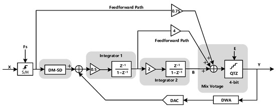
Figure 1.
Block diagram of the proposed second-order feed-forward modulator.
2.2. Analysis of Circuit Non-Ideality
The integrator is the crucial part of the modulator, and the noise of the first integrator is important since its noise cannot be shaped by the loop. The noise mainly includes thermal noise, flicker noise, and power noise. The flicker noise can be reduced by chopper technology.
As mentioned in [16,17], the power/ground noise has a spectrum from several kHz to several GHz. The power/ground noise affects any blocks connected to the power distribution network, such as the amplifier and the comparator array. When the frequency of power/ground noise coupled on ADC circuits is mid-band frequency, the ENOB is decreased by about 0.8 bit [16]. We reduce the influence of power noise by using the linear power supply and coupling capacitance.
The noise model of the integrator is shown in Figure 2,
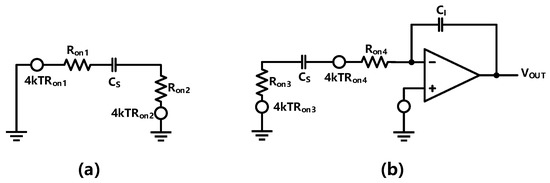
Figure 2.
Noise model of the integrator in (a) sampling phase (b) integrating phase.
Figure 2a shows the noise model of the sampling phase. In this phase, the thermal noise of the two switches can be combined, and the power spectral density on the sampling capacitance can be expressed as:
where is the time constant, k is the Boltzmann constant of J/K, T is the absolute temperature, f is the frequency, is the sampling capacitance, and is the on-resistance of the switch. By integrating the power spectral density over the 3 dB band, and considering the oversampling technology, the noise power in the band is:
The noise model of the integrating phase is shown in Figure 2b. The main noise sources of the integrating phase are the thermal noise from the switches and the amplifier. The amplifier used in the first integrator is a two-stage feedforward miller compensation (FFMC) operational transconductance amplifier (OTA), which can be approximated to a single pole system through careful design. According to [18,19], the noise introduced by the switches can be derived as:
and the noise introduced by the amplifier is:
where is coefficient which can be derived to be equal to 2/3 for long-channel transistors, OSR is the oversampling rate, and is a process-dependent constant. The total input noise of the integrator can be expressed as:
where , if , the noise of the integrator is mainly determined by the thermal noise of the sampling capacitor.
We also performed behavior simulations to evaluate the impact of the non-idealities on the SNDR. The non-ideal factors considered here include the finite gain of the OTA, the KT/C noise of sample switches, slew rate (SR), unity-gain-bandwidth (UGB) of the OTA, and mismatch of the DAC capacitors array.
From the simulation results shown in Figure 3, we can determine the preliminary parameters of the non-ideal factors in the circuit-level design. For example, the finite DC gain of the amplifier should be greater than 60 dB and the sampling capacitance should be greater than 4 pF. Table 1 summarizes the required conditions.
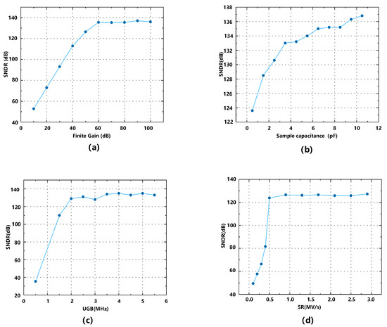
Figure 3.
Impacts of circuit non-idealities to SNDR including (a) finite gain, (b) KT/C noise, (c) unit-gain-bandwidth, and (d) slew rate.

Table 1.
The conditions of non-ideal circuit parameters to obtain required SNDR.
With the conditions in Table 1, the behavior level simulation shows that the structure can achieve 129 dB SNDR at 1500 Hz signal bandwidth.
3. Circuit Analysis and Implementation
The top-level schematic of the proposed modulator is shown in Figure 4. The modulator which is driven by a non-overlapping clock consists of two integrators, the quantizer, and a DAC.
Figure 4.
Top-level schematic of the proposed DT modulator and the non-overlapping clock.
3.1. The Proposed Dynamic-Modulated Scaling-Down (DM-SD) Module
The schematic and timing diagram of the proposed DM-SD module is shown in Figure 5. A scaling factor of 3/4 is introduced to optimize the signal transfer function (STF) to extend the DR. The scaling factor takes into account the cycle length and the impact on the overall modulator. In this paper, we shared the sampling capacitance with the feedback DAC capacitance array, which is divided into 16 units. If the scaling factor is large, such as 15/16, it takes 16 cycles to complete a cycle, and we need to complete it in the shortest time so that the signal is approximately unchanged. However, if it is too small, the performance of the modulator will be degraded. So, 3/4 is selected as the coefficient. We use 12 capacitors for sampling the input signal in each cycle, and the remaining capacitors are free-wheeling (connected to the common mode voltage ). A dynamic modulation technology is used to eliminate coefficient mismatch errors. As shown in Figure 5, in cycle one, capacitors – are selected and capacitors – are free-wheeling. In cycle two, capacitors –– are selected and capacitors – are free-wheeling. In cycle three, capacitors –– are selected, and in cycle four, capacitors – are selected.
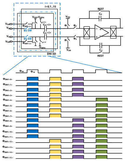
Figure 5.
Schematic and timing diagram of the proposed DM-SD.
The mismatch of the coefficient includes random mismatch and systematic mismatch, assuming that the total element mismatch of the unit is , where is the random mismatch and is the systematic mismatching. The capacitance m can be expressed as , where C is the ideal capacitance unit. As mentioned above, the average coefficient is equal to equation:
From the result, we find that the mismatch of the coefficient can be sufficiently reduced with the proposed DM-SD technology. Furthermore, with the scaling factor of 3/4 introduced by the proposed DM-SD technology, the modulator can withstand full-scale input without being saturated or unstable, leading to extended DR.
3.2. Low Parasitic Capacitor Integrator
The proposed low parasitic capacitor integrator in this paper is shown in Figure 6. For simplicity, we hereby draw the single-ended version instead of the fully differential one in the real implementation.
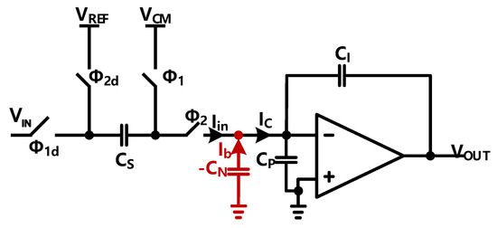
Figure 6.
Schematic of the proposed low parasitic capacitance integrator.
As mentioned in [20,21], the output of the integrator during integration can be derived as:
where , , and the time constant of this equation is , the parasitic capacitance can induce a incomplete setting error. We use a ‘negative’ capacitance which has been merged with the OTA (Figure 7) to reduce the influence of the parasitic capacitance. As shown in Figure 6, the equal parasitic capacitance can be derived. We assume that is the voltage of the negative input of the OTA, is the current flowing to the , is the current from the , and is the equivalent current flowing into the negative node of the OTA. So the can be written as:
so that , with the ‘negative’ capacitance the expression can be rewritten as:
where , thus the influence of the parasitic capacitance on setting error can be reduced. Figure 8 shows the transient response with and without ‘negative’ capacitance.
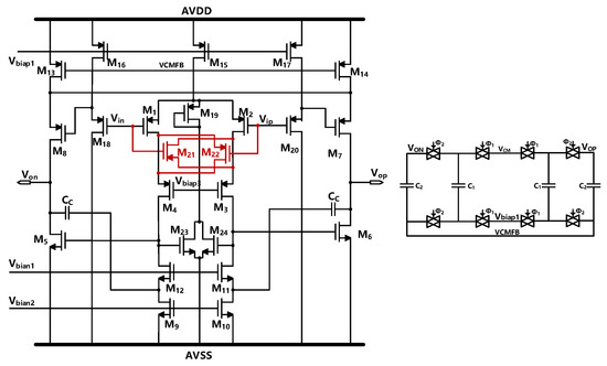
Figure 7.
Schematic of the FFMC OTA used in the first integrator.
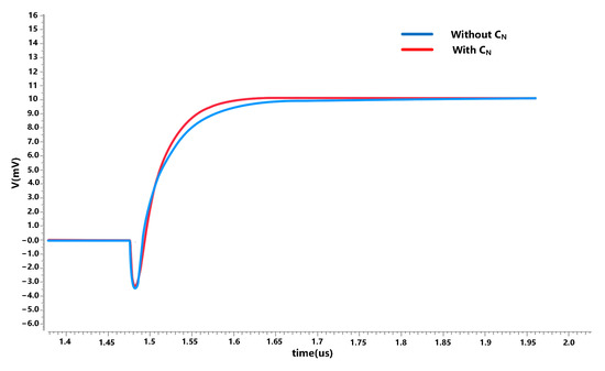
Figure 8.
The output voltage with/without .
The result shows that with the ‘negative’ capacitance the output of the integrator can set up faster. Figure 9 summarizes the improvement in linearity due to this effect at different magnitudes.
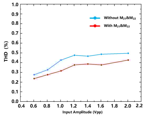
Figure 9.
THD (Total Harmonic Distortion)(%) versus input amplitude with/without .
From Section 2.2, we can conclude that the gain of the amplifier of the first stage integrator should be sufficiently large. We use a cross-coupled FFMC amplifier to obtain higher DC gain [22,23]. The schematic diagram of the amplifier is shown in Figure 7.
To further verify the performance of the first OTA, the specification of gain, PM, IRN, and UGB has been simulated with 27 conditions, including different process corners (tt/ss/ff), temperature (−40/30/80), and voltage (4.8/5/5.2 V). the simulation result is shown in Figure 10. With a 5pF load capacitance, the OTA achieved a 121.71 dB DC gain, 75.49 dB phase-margin, and 20.65 MHz unity-gain-bandwidth with 17.85 nV input-referenced noise. The simulation result shows that the OTA can meet the requirements listed in Table 1 even in the worst case.
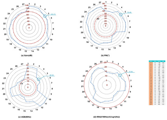
Figure 10.
The PVT simulation result of (a) gain, (b) PM, (c) UGB, and (d) IRN of the opamp.
Since the non-ideal factor of the second stage integrator can be shaped by the loop, the requirement of the second OTA can be significantly relaxed. The telescopic OTA is used to save power consumption. The schematic diagram and simulation results of the OTA are shown in Figure 11. The simulation results show that the gain of the second stage amplifier is greater than 60 dB and the gain bandwidth product is greater than 10 MHz.
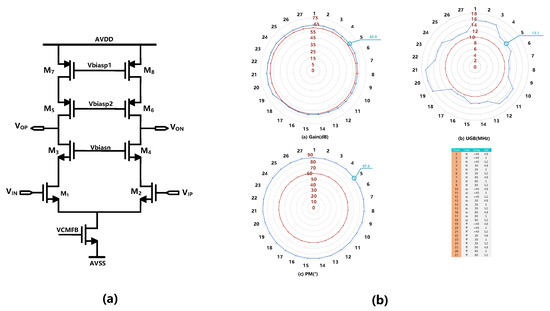
Figure 11.
(a) Schematic of the second OTA. (b) The PVT simulation result of the second OTA.
3.3. The Randomized Data Weighted Averaging (RnDWA)
The use of a multi-bit quantizer will introduce the problem of capacitance mismatch. We use RnDWA technology [24,25] to reduce the influence of capacitance mismatch. The structure diagram of the RnDWA is shown in Figure 12. A simple random number generator circuit is presented, which makes use of the characteristics of the proposed modulator to generate random signals. As shown in Figure 1, the voltage , which is the output voltage of the second integrator, can be expressed as and it is a delay version of the quantization noise which is random noise. The voltage is compared with a reference voltage using a comparator to convert the noise to digital code. Since the accuracy requirement of the comparator is not high, the comparator can be designed with minimum size to save area. Compared with traditional random generation circuits [26,27,28,29], the complexity and the occupied area are reduced. The total additional area for the random generator (including the comparator) is 20 m. Compared with the traditional random generation circuits, the area has been reduce at least 60%.
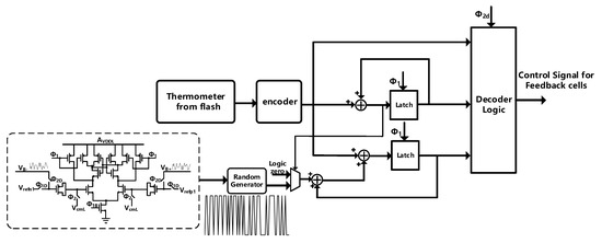
Figure 12.
The structure of RnDWA module.
With the RnDWA, the units of DAC can be selected through the following logic: As with the classical DWA, RnDWA first completes a rotation based on the input sequence and the current pointer. In addition, we then select a random new start point according to the input random number. When this operation is completed, we continue selecting units until we reach the same start point again. Then another new start point is chosen, and so on. For example, we assume that the input sequence is ‘0, 4, 6, 8, 7, 5, 2, 4, 9, 3, 9, 5’, the random number used is ‘3, 4, 9’, and the selected units are shown in Figure 13. The colored square is the currently selected DAC cell and the white is unused.
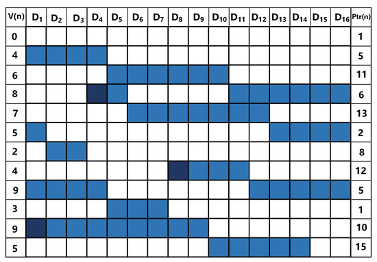
Figure 13.
Demonstration of the RnDWA algorithm, the left-most (V(n)) column is the input data sequence, and the right-most (Ptr (n) ) column is the position of the pointer.
With the RnDWA, the mismatch error of DAC can be reshaped and pushed to high frequency. Taking into account the noise shaping, SNR in baseband for large OSR can be estimated by the following formula [25]:
where M is the number of DAC units, OSR is the oversampling ratio, and is the standard deviation of the random mismatch error of the units. With OSR = 341, M = 16, , a 135 dB in-band SNR can be obtained. Figure 14 shows the PSD of the modulator with and without the RnDWA.
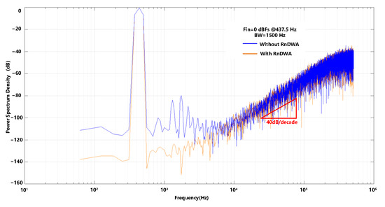
Figure 14.
The power spectrum of the modulator with/without the RnDWA.
3.4. Theoretical Analysis and Implementation of the Voltage Domain Module Technology
The voltage domain technology has been used for saving power consumption of the quantizer and DEM logic circuits. The module makes use of the voltage scaling characteristics of the passive adder. The comparator is shown in Figure 15.
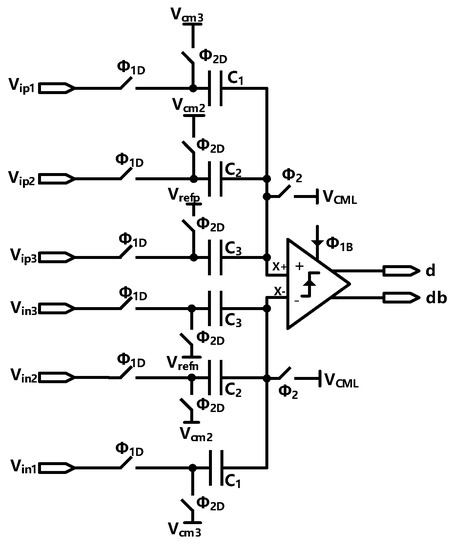
Figure 15.
Schematic of the scaling voltage module.
In phase , the charge stored on the capacitors (take the positive of the comparator for example) can be expressed as:
In the next phase , the charge on the capacitor becomes
Since the charge of the two phase is conserved, the equation can be written:
We choose , and we can derive that:
where is the common mode voltage of the comparator, is the input signal, is the reference of the flash ADC, is the output of the first integrator, is the output of the second integrator, and are the common mode voltage of the output of the first and second integrators, respectively. Because the signal flowing in the loop only contains quantization noise, the output of the integrators is around 500 mV, so the max voltage of is about 1.79 V. thus, the supply voltage of the comparator can be scaled to 1.8 V. and the different voltage of the comparator can be expressed as:
To save power consumption, the dynamic comparator has been used. We performed a Monte Carlo simulation to evaluate the offset of the comparator. The schematic and simulation result is shown in Figure 16.
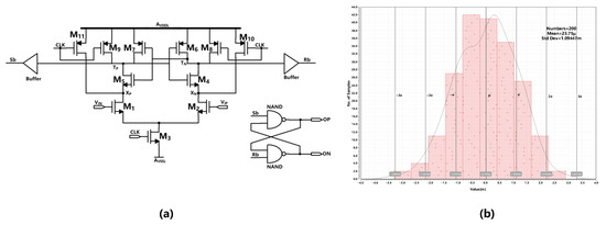
Figure 16.
(a) Schematic of the comparator. (b) The Monte Carlo simulation result of the comparator’s offset.
The simulation result shows that the mean offset voltage is 23.75 uV, and the (standard deviation of the offset) is 1.09 mV. As mentioned in [30], in order to control the error probability, the minimum resolution of the comparator should be greater than six times of the offset. The minimum resolution of the quantizer in this design is 112.5 mV which has a sufficient margin.
4. Results
The proposed sigma-delta modulator shown in Figure 17 is designed using 180 nm CMOS technology, occupying 0.49 mm. Figure 18 shows the power spectrum with and without the DM-SD technology simulated with transient noise at a full-scale signal input (0 dBFS). The simulation results show that with a 0 dBFS, 437.5 Hz input signal, and 1500 Hz signal bandwidth, a 118.1 dB SNDR can be obtained. Figure 19a shows the SNDR versus the input amplitude with and without the DM-SD. The result shows that with the DM-SD technology, the DR can be extended to 126 dB. The power consumption diagram is shown in Figure 19b. Due to the use of voltage domain technology, the power consumption of the quantizer and the DEM circuit is reduced by about 30%. The total power consumption of the modulator is 1.6 mW. Table 2 compares the result of this work to state-of-the-art works. Among the listed reference, it is evident that our modulator achieves the highest SNDR (118.1 dB) and DR (126 dB). To evaluate the overall performance of the proposed ADC, Figure of Merit (FoMs) is used. It shows that our modulator achieves a competitive FoMs (177.8 dB) compared with other works.
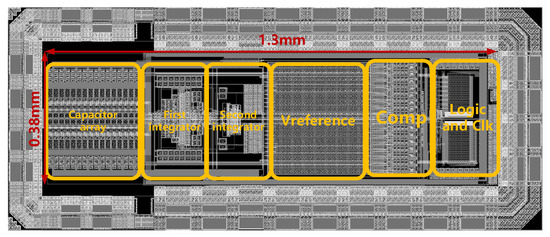
Figure 17.
The layout circuit of the proposed modulator.
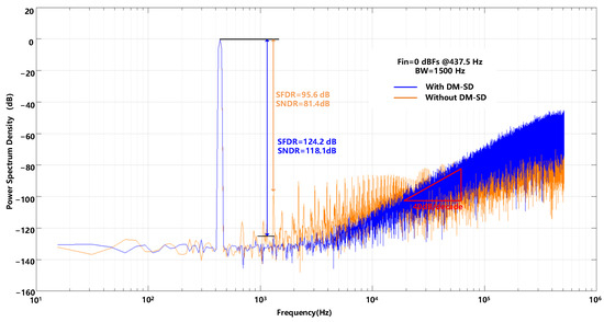
Figure 18.
The power spectrum of the proposed modulator simulated with transient noise.
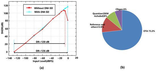
Figure 19.
(a) SNDR versus input amplitude with/without DM-SD. (b) Total power consumption breakdown among circuit blocks.
Table 2.
Performance summary and comparison with previous works.
5. Conclusions
In this paper, we propose a wide dynamic range and high-resolution discrete-time 2-order 4-bit sigma-delta modulator for non-invasive electroencephalogram acquisition. The modulator is designed with 180nm CMOS technology occupying a 0.49 mm area. A novel dynamic-modulated scaling-down technology has been proposed to extend the DR of the modulator. With the DM-SD technology, We achieve a 126 dB DR. We use the RnDWA and the low parasitic capacitance integrator technologies to optimize the performance of the modulator. With these techniques, we achieve a 118.1 dB SNDR. The total power consumption of the modulator is 1.6 mW, which benefits from the VDT technology, and a competitive FoMs (177.8 dB) is achieved.
Author Contributions
Conceptualization, Y.H., X.W. and Y.L.; methodology, Y.H., X.W. and X.Z.; software, Y.H., W.L. and X.Z.; formal analysis, Y.H.; investigation, Y.H. and W.L; writing—original draft preparation, Y.H. and X.L.; writing—review and editing, Y.H., W.L. and X.W.; supervision, X.W. and Y.L. All authors have read and agreed to the published version of the manuscript.
Funding
This work was supported by the National Key Research and Development Program of China under Grant number 2021YFF1200600.
Institutional Review Board Statement
Not applicable.
Informed Consent Statement
Not applicable.
Acknowledgments
The authors would like to thank Mingyi Chen and Kaiquan Chen in Shanghai Jiao Tong University, and SE. Shunping Wang for their valuable discussions and comments.
Conflicts of Interest
The authors declare no conflict of interest. The funders had no role in the design of the study; in the collection, analyses, or interpretation of data; in the writing of the manuscript, or in the decision to publish the results.
Abbreviations
The following abbreviations are used in this manuscript:
| ADC | Analog to Digital Converter |
| AFE | Analog Front End |
| BCI | Brain Computer Interface |
| CT | Continue Time |
| CMFB | Common Mode Feedback |
| CMOS | Complementary Metal-Oxide-Semiconductor Transistor |
| DAC | Digital to Analog Converter |
| DEM | Dynamic Element Match |
| RnDWA | Randomized Data Weighted Averaging |
| DM-SD | Dynamic-Modulated Scaling-Down |
| DR | Dynamic Range |
| DT | Discrete Time |
| EEG | electroencephalogram |
| ENOB | Effective Number of Bits |
| FFMC | Feed-Forward Miller Compensation |
| OSR | Over-Sampling Ratio |
| OTA | Operational Transconductance Amplifier |
| PVT | Power, Voltage, and Temperature |
| SNR | Signal-to-Noise Ratio |
| SNDR | Signal-to-Noise plus Distortion Ratio |
| SAR | Successive Approximation Register |
| STF | Signal Transfer Function |
| SR | Slew Rate |
| THD | Total Harmonic Distortion |
| UGB | Unity Gain bandwidth |
| VDT | Voltage Domain Technology |
References
- Gu, X.; Cao, Z.; Jolfaei, A.; Xu, P.; Wu, D.; Jung, T.P.; Lin, C.T. EEG-based brain-computer interfaces (BCIs): A survey of recent studies on signal sensing technologies and computational intelligence approaches and their applications. IEEE/ACM Trans. Comput. Biol. Bioinform. 2021, 18, 1645–1666. [Google Scholar] [CrossRef] [PubMed]
- Zeng, H.; Yang, C.; Dai, G.; Qin, F.; Zhang, J.; Kong, W. EEG classification of driver mental states by deep learning. Cogn. Neurodyn. 2018, 12, 597–606. [Google Scholar] [CrossRef]
- McKay, J.H.; Feyissa, A.M.; Sener, U.; D’Souza, C.; Smelick, C.; Spaulding, A.; Yelvington, K.; Tatum, W.O. Time is brain: The use of EEG electrode caps to rapidly diagnose nonconvulsive status epilepticus. J. Clin. Neurophysiol. 2019, 36, 460–466. [Google Scholar] [CrossRef] [PubMed]
- Lin, C.T.; Chuang, C.H.; Huang, C.S.; Tsai, S.F.; Lu, S.W.; Chen, Y.H.; Ko, L.W. Wireless and Wearable EEG System for Evaluating Driver Vigilance. IEEE Trans. Biomed. Circuits Syst. 2014, 8, 165–176. [Google Scholar] [CrossRef] [PubMed]
- Vaid, S.; Singh, P.; Kaur, C. EEG Signal Analysis for BCI Interface: A Review. In Proceedings of the 2015 Fifth International Conference on Advanced Computing Communication Technologies, Rohtak, India, 21–22 February 2015; pp. 143–147. [Google Scholar] [CrossRef]
- Tohidi, M.; Madsen, J.K.; Moradi, F. Low-power high-input-impedance EEG signal acquisition SoC with fully integrated IA and signal-specific ADC for wearable applications. IEEE Trans. Biomed. Circuits Syst. 2019, 13, 1437–1450. [Google Scholar] [CrossRef] [PubMed]
- Huang, J.; Mercier, P.P. A 112-dB SFDR 89-dB SNDR VCO-Based Sensor Front-End Enabled by Background-Calibrated Differential Pulse Code Modulation. IEEE J. Solid-State Circuits 2021, 56, 1046–1057. [Google Scholar] [CrossRef]
- Ibrahim, O.; Hesham, R.; Soltan, A. A 26.24uW 9.26-ENOB Dynamic RAM Based SAR ADC for Biomedical Applications. In Proceedings of the 2020 32nd International Conference on Microelectronics (ICM), Aqaba, Jordan, 14–17 December 2020; pp. 1–4. [Google Scholar] [CrossRef]
- Verma, D.; Rikan, B.S.; Shehzad, K.; Kim, S.J.; Khan, D.; Kommangunta, V.; Shah, S.A.A.; Pu, Y.; Yoo, S.S.; Hwang, K.C.; et al. A Design of 44.1 fJ/Conv-Step 12-Bit 80 ms/s Time Interleaved Hybrid Type SAR ADC With Redundancy Capacitor and On-Chip Time-Skew Calibration. IEEE Access 2021, 9, 133143–133155. [Google Scholar] [CrossRef]
- Yang, X.; Zhao, M.; Dong, Y.; Wu, X. A 14.9μW analog front-end with capacitively-coupled instrumentation amplifier and 14-bit SAR ADC for epilepsy diagnosis system. In Proceedings of the 2016 IEEE Biomedical Circuits and Systems Conference (BioCAS), Shanghai, China, 17–19 October 2016; pp. 268–271. [Google Scholar] [CrossRef]
- Wang, S.H.; Hung, C.C. A 0.3V 10b 3MS/s SAR ADC With Comparator Calibration and Kickback Noise Reduction for Biomedical Applications. IEEE Trans. Biomed. Circuits Syst. 2020, 14, 558–569. [Google Scholar] [CrossRef]
- Shu, Y.S.; Kuo, L.T.; Lo, T.Y. An Oversampling SAR ADC With DAC Mismatch Error Shaping Achieving 105 dB SFDR and 101 dB SNDR Over 1 kHz BW in 55 nm CMOS. IEEE J. Solid-State Circuits 2016, 51, 2928–2940. [Google Scholar] [CrossRef]
- Gerfers, F.; Ortmanns, M.; Manoli, Y. A 1.5-V 12-bit power-efficient continuous-time third-order ΔΣ modulator. IEEE J. Solid-State Circuits 2003, 38, 1343–1352. [Google Scholar] [CrossRef]
- Bang, J.S.; Jeon, H.; Je, M.; Cho, G.H. 6.5µW 92.3DB-DR Biopotential-Recording Front-End with 360MVPP Linear Input Range. In Proceedings of the 2018 IEEE Symposium on VLSI Circuits, Honolulu, HI, USA, 18–22 June 2018; pp. 239–240. [Google Scholar] [CrossRef]
- Song, S.; Kim, J.; Roh, J. 100.5 dB SNDR Analog Front-End With a Resistor-Based Discrete-Time Delta-Sigma Modulator for Eliminating Switching Noise and Harmonics. IEEE Access 2021, 9, 39852–39863. [Google Scholar] [CrossRef]
- Ahn, W.; Shim, J.; Cho, J.; Shin, M.; Koo, K.; Kim, J. Analysis of power/ground noise effect on performance degradation of analog-to-digital converter. In Proceedings of the 2009 11th Electronics Packaging Technology Conference, Singapore, 9–11 December 2009; pp. 687–691. [Google Scholar]
- Bae, B.; Shim, Y.; Koo, K.; Cho, J.; Pak, J.S.; Kim, J. Modeling and measurement of power supply noise effects on an analog-to-digital converter based on a chip-PCB hierarchical power distribution network analysis. IEEE Trans. Electromagn. Compat. 2013, 55, 1260–1270. [Google Scholar] [CrossRef]
- Schreier, R.; Silva, J.; Steensgaard, J.; Temes, G.C. Design-oriented estimation of thermal noise in switched-capacitor circuits. IEEE Trans. Circuits Syst. I Regul. Pap. 2005, 52, 2358–2368. [Google Scholar] [CrossRef]
- Huang, L.; Shen, J.; Ma, Q.; Wang, H.; Tsang, W.M.; Tang, F.; Wang, M. A Low-Noise and Monolithic Array Tactile Sensor Based on Incremental Delta-Sigma Analog-to-Digital Converters. Electronics 2022, 11, 1206. [Google Scholar] [CrossRef]
- Del Rio, R.; Medeiro, F.; Pérez-Verdú, B.; Rodríguez-Vázquez, A. Reliable analysis of settling errors in SC integrators: Application to [Sigma][Delta] modulators. Electron. Lett. 2000, 36, 1. [Google Scholar] [CrossRef]
- De la Rosa, J.M.; del Río, R. Circuits and Errors: Systematic Analysis and Practical Design Issues. In CMOS Sigma-Delta Converters; John Wiley & Sons, Ltd.: Hoboken, NJ, USA, 2013. [Google Scholar] [CrossRef]
- Lee, H.S.; Gealow, J.; Yoon, D.Y. Power-efficient amplifier frequency compensation for continuous-time delta-sigma modulators. In Proceedings of the 2013 IEEE 56th International Midwest Symposium on Circuits and Systems (MWSCAS), Columbus, OH, USA, 4–7 August 2013; pp. 562–565. [Google Scholar]
- Chen, K.; Chen, M.; Cheng, L.; Qi, L.; Wang, G.; Lian, Y. A 124 dB dynamic range sigma-delta modulator applied to non-invasive EEG acquisition using chopper-modulated input-scaling-down technique. Sci. China Inf. Sci. 2022, 65, 1–15. [Google Scholar] [CrossRef]
- Kim, Y.G.; Cho, M.H.; Kim, K.D.; Kwon, J.K.; Kim, J. A 105.55 dB, 0.49 mm 2 Audio ΣΔ modulator using chopper stabilization and fully randomized DWA. In Proceedings of the 2008 IEEE Custom Integrated Circuits Conference, San Jose, CA, USA, 21–24 September 2008; pp. 503–506. [Google Scholar]
- Vadipour, M. Techniques for preventing tonal behavior of data weighted averaging algorithm in/spl Sigma/-/spl Delta/modulators. IEEE Trans. Circuits Syst. II Analog Digit. Signal Process. 2000, 47, 1137–1144. [Google Scholar] [CrossRef]
- Brederlow, R.; Prakash, R.; Paulus, C.; Thewes, R. A low-power true random number generator using random telegraph noise of single oxide-traps. In Proceedings of the 2006 IEEE International Solid State Circuits Conference, San Francisco, CA, USA, 6–9 February 2006; pp. 1666–1675. [Google Scholar] [CrossRef]
- Figliolia, T.; Julian, P.; Tognetti, G.; Andreou, A.G. A true Random Number Generator using RTN noise and a sigma delta converter. In Proceedings of the 2016 IEEE International Symposium on Circuits and Systems (ISCAS), Montreal, QC, Canada, 22–25 May 2016; pp. 17–20. [Google Scholar] [CrossRef]
- Petrie, C.; Connelly, J. A noise-based IC random number generator for applications in cryptography. IEEE Trans. Circuits Syst. I Fundam. Theory Appl. 2000, 47, 615–621. [Google Scholar] [CrossRef]
- Hua Zhou, S.; Zhang, W.; Wu, N.J. An ultra-low power CMOS random number generator. Solid-State Electron. 2008, 52, 233–238. [Google Scholar] [CrossRef]
- Nuzzo, P.; De Bernardinis, F.; Terreni, P.; Van der Plas, G. Noise analysis of regenerative comparators for reconfigurable ADC architectures. IEEE Trans. Circuits Syst. I Regul. Pap. 2008, 55, 1441–1454. [Google Scholar] [CrossRef]
- Lv, R.; Chen, W.; Yin, L.; Fu, Q.; Liu, X.; Yan, J. A closed-loopΣΔmodulator for micromechanical capacitive sensors. IEICE Electron. Express 2018, 15, 20171112. [Google Scholar] [CrossRef]
- Chen, X.; Wang, Z.G.; Li, F. A 3rd-order 1-bit Σ-Δ modulator with a 2-tap FIR filter embedded. IEICE Electron Express 2019, 16, 20190365. [Google Scholar] [CrossRef]
- Han, J.H.; Cho, K.I.; Kim, H.J.; Boo, J.H.; Kim, J.S.; Ahn, G.C. A 96dB Dynamic Range 2kHz Bandwidth 2nd Order Delta-Sigma Modulator Using Modified Feed-Forward Architecture With Delayed Feedback. IEEE Trans. Circuits Syst. II Express Briefs 2021, 68, 1645–1649. [Google Scholar] [CrossRef]


Disclaimer/Publisher’s Note: The statements, opinions and data contained in all publications are solely those of the individual author(s) and contributor(s) and not of MDPI and/or the editor(s). MDPI and/or the editor(s) disclaim responsibility for any injury to people or property resulting from any ideas, methods, instructions or products referred to in the content. |
© 2022 by the authors. Licensee MDPI, Basel, Switzerland. This article is an open access article distributed under the terms and conditions of the Creative Commons Attribution (CC BY) license (https://creativecommons.org/licenses/by/4.0/).