
A Study on the Effect of Temperature Variations on FPGA-Based Multi-Channel Time-to-Digital Converters


Abstract
:1. Introduction
2. Methodology
- Voltage variations: The core voltage for most modern FPGAs is within the range of 1.2–1.5 volts [39,40,41,42,43]. Although the voltage threshold can be regulated using the built-in voltage regulators on the FPGA devices, in some conditions, a small variation of a few millivolts can impact the TDC accuracy.
2.1. Specifications of Selected FPGAs
2.2. The Proposed TDL TDC
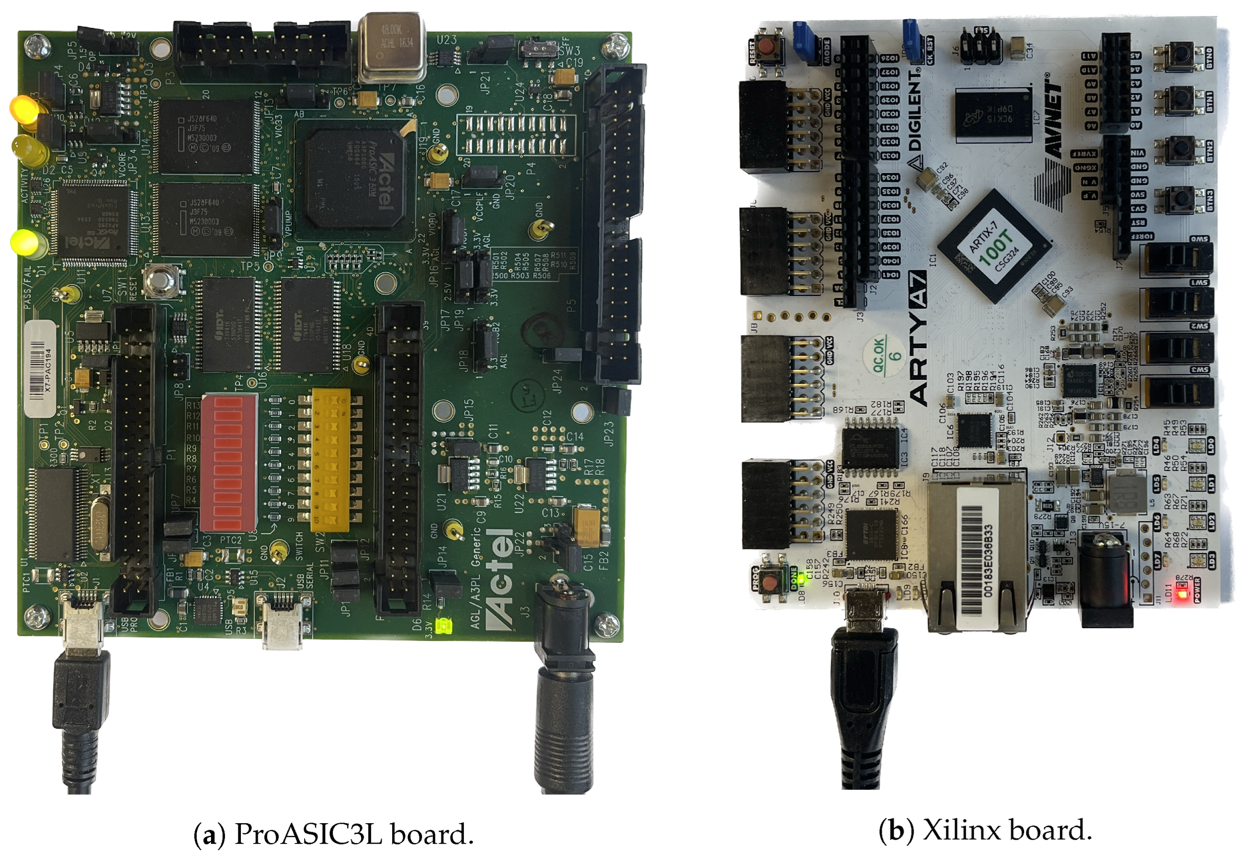
2.3. Tapped Delay Line (TDL) on Xilinx and ProASIC3L FPGA Boards
2.4. Xilinx FPGA-Based TDL TDC
2.5. ProASIC3L FPGA-Based TDL TDC
2.6. Encoder
3. Time Measurement Algorithms
Averaging Process
4. Implementation
4.1. Implementation on Xilinx FPGA
4.2. Implementation of TDC on ProASIC3L
5. Results and Discussion
5.1. Statistical Analysis of the Proposed TDL TDC on Both FPGAs
5.2. Thermal Variation Analysis
5.3. Power Consumption Analysis
6. Conclusions
Author Contributions
Funding
Institutional Review Board Statement
Informed Consent Statement
Data Availability Statement
Conflicts of Interest
References
- Malin, M.C.; Bell, J.F.; Cantor, B.A.; Caplinger, M.A.; Calvin, W.M.; Clancy, R.T.; Edgett, K.S.; Edwards, L.; Haberle, R.M.; James, P.B.; et al. Context Camera Investigation on board the Mars Reconnaissance Orbiter. J. Geophys. Res. Planets 2007, 112, 1–25. [Google Scholar] [CrossRef]
- Wood, P.B.; Furman, J.D. The impact of complexity growth on instrument reliability: A case study of Cassini IMS and MMS HPCA. In Proceedings of the 2018 IEEE Aerospace Conference, Big Sky, MT, USA, 3–10 March 2018; pp. 1–11. [Google Scholar]
- Calvo, R.M.; Poliak, J.; Surof, J.; Wolf, R. Evaluation of optical ranging and frequency transfer for the Kepler system: PPreliminary laboratory tests. In Proceedings of the 2020 European Navigation Conference, ENC 2020, Dresden, Germany, 23–24 November 2020; pp. 1–9. [Google Scholar] [CrossRef]
- Li, D.; Liu, M.; Ma, R.; Zhu, Z. An 8-ch LIDAR Receiver Based on TDC with Multi-Interval Detection and Real-Time in SituCalibration. IEEE Trans. Instrum. Meas. 2020, 69, 5081–5090. [Google Scholar] [CrossRef]
- Fan, H.; Feng, C.; Sun, W.; Yin, C.; Liu, S.; An, Q. A high-density time-to-digital converter prototype module for BES III end-cap TOF upgrade. IEEE Trans. Nucl. Sci. 2013, 60, 3563–3569. [Google Scholar] [CrossRef]
- Hejazi, A.; Oh, S.; Rehman, M.R.U.; Rad, R.E.; Kim, S.; Lee, J.; Pu, Y.; Hwang, K.C.; Yang, Y.; Lee, K.Y. A Low-Power Multichannel Time-to-Digital Converter Using All-Digital Nested Delay-Locked Loops with 50-ps Resolution and High Throughput for LiDAR Sensors. IEEE Trans. Instrum. Meas. 2020, 69, 9262–9271. [Google Scholar] [CrossRef]
- Neiser, A.; Adamczewski-Musch, J.; Hoek, M.; Koenig, W.; Korcyl, G.; Linev, S.; Maier, L.; Michel, J.; Palka, M.; Penschuck, M.; et al. TRB3: A 264 channel high precision TDC platform and its applications. J. Instrum. 2013, 8, C12043. [Google Scholar] [CrossRef]
- Alshahry, S.M.; Alshehry, A.H.; Alhazmi, A.K.; Chodavarapu, V.P. A Size, Weight, Power, and Cost-Efficient 32-Channel Time to Digital Converter Using a Novel Wave Union Method. Sensors 2023, 23, 6621. [Google Scholar] [CrossRef]
- Zhao, L.; Hu, X.; Liu, S.; Wang, J.; Shen, Q.; Fan, H.; An, Q. The design of a 16-channel 15 ps TDC implemented in a 65 nm FPGA. IEEE Trans. Nucl. Sci. 2013, 60, 3532–3536. [Google Scholar] [CrossRef]
- Cheng, Z.; Zheng, X.; Deen, M.J.; Peng, H. Recent developments and design challenges of high-performance ring oscillator CMOS time-to-digital converters. IEEE Trans. Electron. Dev. 2015, 63, 235–251. [Google Scholar] [CrossRef]
- Garzetti, F.; Corna, N.; Lusardi, N.; Geraci, A. Time-to-Digital Converter IP-Core for FPGA at State of the Art. IEEE Access 2021, 9, 85515–85528. [Google Scholar] [CrossRef]
- Bayer, E.; Traxler, M. A high-resolution (<10 ps RMS) 32-channel time-to-digital converter (TDC) implemented in a field programmable gate array (FPGA). In Proceedings of the 2010 17th IEEE-NPSS Real Time Conference, Lisbon, Portugal, 24–28 May 2010; pp. 1–5. [Google Scholar]
- Machado, R.; Cabral, J.; Alves, F.S. Recent developments and challenges in FPGA-based time-to-digital converters. IEEE Trans. Instrum. Meas. 2019, 68, 4205–4221. [Google Scholar] [CrossRef]
- Tancock, S.; Arabul, E.; Dahnoun, N. A review of new time-to-digital conversion techniques. IEEE Trans. Instrum. Meas. 2019, 68, 3406–3417. [Google Scholar] [CrossRef]
- Mattada, M.P.; Guhilot, H. Time-to-digital converters—A comprehensive review. Int. J. Circuit Theory Appl. 2021, 49, 778–800. [Google Scholar] [CrossRef]
- Qin, X.; Wang, L.; Liu, D.; Zhao, Y.; Rong, X.; Du, J. A 1.15-ps Bin Size and 3.5-ps Single-Shot Precision Time-to-Digital Converter With On-Board Offset Correction in an FPGA. IEEE Trans. Nucl. Sci. 2017, 64, 2951–2957. [Google Scholar] [CrossRef]
- Matrix, M. A 7.4 ps FPGA-Based TDC with a 1024-Unit Measurement Matrix. Sensors 2017, 17, 865. [Google Scholar] [CrossRef]
- Szyduczyński, J.; Kościelnik, D.; Miśkowicz, M. A successive approximation time-to-digital converter with single set of delay lines for time interval measurements. Sensors 2019, 19, 1109. [Google Scholar] [CrossRef]
- Henzler, S. Time-to-Digital Converters; Springer: Dordrecht, The Netherlands, 2010; Volume 29. [Google Scholar] [CrossRef]
- Won, J.Y.; Kwon, S.I.; Yoon, H.S.; Ko, G.B.; Son, J.W.; Lee, J.S. Dual-phase tapped-delay-line time-to-digital converter with on-the-fly calibration implemented in 40 nm FPGA. IEEE Trans. Biomed. Circuits Syst. 2015, 10, 231–242. [Google Scholar] [CrossRef] [PubMed]
- Favi, C.; Charbon, E. A 17 ps Time-to-Digital Converter Implemented in 65 nm Technology; ACM Press: New York, NY, USA, 2009; pp. 113–120. [Google Scholar] [CrossRef]
- Song, J.; An, Q.; Liu, S. A high-resolution time-to-digital converter implemented in field-programmable-gate-arrays. IEEE Trans. Nucl. Sci. 2006, 53, 236–241. [Google Scholar] [CrossRef]
- Qin, X.; Feng, C.; Zhang, D.; Miao, B.; Zhao, L.; Hao, X.; Liu, S.; An, Q. Development of a High Resolution TDC for Implementation in Flash-Based and Anti-Fuse FPGAs for Aerospace Application. IEEE Trans. Nucl. Sci. 2013, 60, 3550–3556. [Google Scholar] [CrossRef]
- Nogrette, F.; Heurteau, D.; Chang, R.; Bouton, Q.; Westbrook, C.; Sellem, R.; Clément, D. Characterization of a detector chain using a FPGA-based time-to-digital converter to reconstruct the three-dimensional coordinates of single particles at high flux. Rev. Sci. Instrum. 2015, 86, 113105. [Google Scholar] [CrossRef]
- Zheng, J.; Cao, P.; Jiang, D.; An, Q. Low-cost FPGA TDC with high resolution and density. IEEE Trans. Nucl. Sci. 2017, 64, 1401–1408. [Google Scholar] [CrossRef]
- Szplet, R.; Kalisz, J.; Szymanowski, R. Interpolating time counter with 100 ps resolution on a single FPGA device. IEEE Trans. Instrum. Meas. 2000, 49, 879–883. [Google Scholar] [CrossRef]
- Wang, J.; Liu, S.; Shen, Q.; Li, H.; An, Q. A fully fledged TDC implemented in field-programmable gate arrays. IEEE Trans. Nucl. Sci. 2010, 57, 446–450. [Google Scholar] [CrossRef]
- Qin, X.; Feng, C.; Zhao, L.; Zhang, D.; Liu, S.; Hao, X.; An, Q. Development of high resolution TDC implemented in radiation tolerant FPGAs for aerospace application. In Proceedings of the 2012 18th IEEE-NPSS Real Time Conference, Berkeley, CA, USA, 9–15 June 2012; pp. 1–5. [Google Scholar] [CrossRef]
- Qin, X.; Feng, C.; Zhang, D.; Zhao, L.; Liu, S.; An, Q. A low dead time vernier delay line TDC implemented in an actel flash-based FPGA. Nucl. Sci. Tech. 2013, 24. [Google Scholar]
- Torres, J.; Aguilar, A.; Garcia-Olcina, R.; Martı, P.; Martos, J.; Soret, J.; Benlloch, J.; Conde, P.; Gonzalez, A.; Sanchez, F.; et al. Time-to-digital converter based on FPGA with multiple channel capability. IEEE Trans. Nucl. Sci. 2013, 61, 107–114. [Google Scholar] [CrossRef]
- Pan, W.; Gong, G.; Li, J. A 20-ps time-to-digital converter (TDC) implemented in field-programmable gate array (FPGA) with automatic temperature correction. IEEE Trans. Nucl. Sci. 2014, 61, 1468–1473. [Google Scholar] [CrossRef]
- Xiang, T.; Zhao, L.; Jin, X.; Wang, T.; Chu, S.; Ma, C.; Liu, S.; An, Q. A 56-ps multi-phase clock time-to-digital convertor based on Artix-7 FPGA. In Proceedings of the 2014 19th IEEE-NPSS Real Time Conference, Nara, Japan, 26–30 May 2014; pp. 1–4. [Google Scholar]
- Wang, Y.; Cao, Q.; Liu, C. A multi-chain merged tapped delay line for high precision time-to-digital converters in FPGAs. IEEE Trans. Circuits Syst. II Express Briefs 2017, 65, 96–100. [Google Scholar] [CrossRef]
- Yang, D.; Cao, Z.; Hao, X.J.; Li, Y.R.; Liu, S.B.; Feng, C.Q.; An, Q. Readout electronics of a prototype time-of-flight ion composition analyzer for space plasma. Nucl. Sci. Tech. 2018, 29, 60. [Google Scholar] [CrossRef]
- Song, Z.; Zhao, Z.; Yu, H.; Yang, J.; Zhang, X.; Sui, T.; Xu, J.; Xie, S.; Huang, Q.; Peng, Q. An 8.8 ps RMS resolution time-to-digital converter implemented in a 60 nm FPGA with real-time temperature correction. Sensors 2020, 20, 2172. [Google Scholar] [CrossRef]
- Deng, J.; Yin, P.; Lei, X.; Shu, Z.; Tang, M.; Tang, F. A tunable parameter, high linearity time-to-digital converter implemented in 28-nm FPGA. IEEE Trans. Instrum. Meas. 2021, 70, 1–12. [Google Scholar] [CrossRef]
- Mao, X.; Yang, F.; Wei, F.; Shi, J.; Cai, J.; Cai, H. A Low Temperature Coefficient Time-to-Digital Converter with 1.3 ps Resolution Implemented in a 28 nm FPGA. Sensors 2022, 22, 2306. [Google Scholar] [CrossRef]
- Kang, M.; Burm, J. Time-domain temperature sensor using two stage vernier type time to digital converter for mobile application. In Proceedings of the ISOCC 2012—2012 International SoC Design Conference, Jeju Island, Republic of Korea, 4–7 November 2012; pp. 431–434. [Google Scholar] [CrossRef]
- Microchip, Inc. ProASIC PLUS® Flash Family FPGAs. 2008, pp. 1–183. Available online: https://www.microsemi.com/document-portal/docview/131796-proasicplusgendes (accessed on 1 July 2023).
- Xilinx. 7 Series FPGAs Configurable Logic Block. Xilinx 2016, UG474, 1–74. Available online: https://www.xilinx.com/support/documentation/user_guides/ug474_7Series_CLB.pdf (accessed on 1 July 2023).
- Xilinx 7 Series FPGA Libraries. 2012, Voume 799, pp. 1–653. Available online: https://www.xilinx.com/htmldocs/xilinx14_7/7series_scm.pdf (accessed on 1 July 2023).
- Digilent, Inc. Arty-A7 Reference Manual. Available online: https://digilent.com/reference/programmable-logic/arty-a7/reference-manual (accessed on 1 July 2023).
- Xilinx, Inc. Vivado Design Suite User Guide. Ug903 2015, 4, 1–173. Available online: http://www.xilinx.com/support/documentation/sw_manuals/xilinx2015_4/ug903-vivado-using-constraints.pdf (accessed on 1 July 2023).
- Xiao, Y.; Zhang, Z.; Duraij, M.S.; Zsurzsan, T.G.; Andersen, M.A. Review of High-Temperature Power Electronics Converters. IEEE Trans. Power Electron. 2022, 37, 14831–14849. [Google Scholar] [CrossRef]
- Tancock, S.; Rarity, J.; Dahnoun, N. Temperature characterisation of the DSP delay line. In Proceedings of the 2021 7th International Conference on Event-Based Control, Communication, and Signal Processing (EBCCSP), Virtual Event, 23–25 June 2021; pp. 1–8. [Google Scholar]


| Platform Type | Pros | Cons |
|---|---|---|
| FPGA | Re-configuration of the TDCs without requiring hardware changes. | Require higher power consumption. |
| High performance using high-speed digital signal processing techniques. | ||
| Easier to customize the TDCs to meet specific application requirements. | ||
| Lower cost, particularly if fewer FPGA resources are required to implement the TDCs. | ||
| Shorter development time. | ||
| ASIC | Fully customized for optimum performance of the TDC for a specific application. | Lack of flexibility; ASICs cannot be reconfigured or modified once they are fabricated. |
| Can be designed to minimize power consumption. | ASIC development is more expensive in low-volume production. | |
| ASIC designs are time-consuming processes, particularly if the designs are large or complex. |
| Ref | Method | Device | RMS [ps] | Precision [ps] | Dead Time [ns] | Temperature Correction | Temperature Range [°C] | Temperature Sensitivity [ps/°C] | Power Consumption [W] |
|---|---|---|---|---|---|---|---|---|---|
| [26] | DL 1 | ProASIC2 | 100 | 70 | NA 2 | NA | [−20–60] | 0.5 | 0.260 |
| [22] | LSPM 3 | Kintex-7 | 1.29 | 3.54 | NA | NA | [10–30] | NA | 0.453 |
| [27] | Counter-interpolator | Virtex-4 | 25 | 50 | 10 | Automatic | [31–61] | 0.047 | NA |
| [28] | Counter-interpolator | A3PE1500 | 150 | 440 | 25 | Automatic | [25–50] | 0.6 | 1 |
| [29] | VDL | A3PE1500 | 42 | 16.4 | 200 | Automatic | [−5–55] | NA | NA |
| [23] | Counter-interpolator | A3PE1500 | 127 | 427 | 25 | Automatic | [−21–71] | 0.56 | 0.050 |
| [30] | TDL | Kintex-7 | 85.7 | NA | 30 | Automatic | [35–75] | 0.5 | NA |
| [31] | TDL WU 4 | Cyclone II | 21.8 | 30.9 | NA | Automatic | [10–70] | NA | NA |
| [32] | TDL | Artix-7 | 56 | 156 | NA | NA | NA | NA | 43 |
| [20] | TDL | Virtex-6 | 10 | 12.8 | 20 | Real-Time | [10–50] | NA | NA |
| [24] | TDL | Virtex-4 | 120 | NA | 7 | NA | [45–85] | 6 | NA |
| [25] | TDL | Artix-7 | 15 | 28 | 10 | NA | [25–85] | NA | NA |
| [33] | Merged DL | Kintex-7 | 4.3 | NA | 50 | NA | [40–70] | 0.64 | NA |
| [34] | TDL | APA1000 | 550 | 180 | 6400 | NA | NA | NA | NA |
| [35] | NUMP 5 | Cyclone 10 | 8.8 | NA | NA | Automatic | [5–80] | 0.054 | 0.039 |
| [36] | NUMMP 6 | Kintex-7 | 1.87 | 2.79 | 8 | Re-TSM 7 | [20–60] | NA | 0.740 |
| [37] | MCS 8 | Kintex-7 | 1.3 | 4.6 | 8 | Self-adaptation | [25–70] | 0.0002 | 0.563 |
| This work | TDL | Artix-7 | 24.7 | 35 | 10 | Automatic | [−75–80] | 0.0338 | 0.968 |
| TDL | APA1000 | 554.59 | 784.31 | 1 | Automatic | [−75–80] | 0 | <0.002 |
| Specifications | ProASIC3L | Xilinx Artix-7 |
|---|---|---|
| FPGA Part Number | M1A3P1000L-FGG484 | XC7A100TCSG324-1 |
| Oscillator for system CLK | Yes | Yes |
| Powered using USB cable | Yes | Yes |
| Logic cells | 1,000,000 | 101,440 |
| Memory devices | 4 MB of SRAM | 4860 kbits |
| 16 MB of flash memory | ||
| Supported by | Libero SoC 1 v11.9 SP6 | Xilinx’s Vivado v2021.1 |
| Radiation-tolerant technology | Yes | No |
| Power | Ultra-Low | Low |
| On-chip XADC 2 | NA | Yes |
| Resource | Utilization | Available | Utilization % |
|---|---|---|---|
| LUT 1 | 11,909 | 63,400 | 18.78 |
| LUTRAM 2 | 410 | 19,000 | 2.16 |
| FF 3 | 54,114 | 126,800 | 42.68 |
| BRAM 4 | 18.5 | 13.70 | 13.7 |
| MMCM 5 | 1 | 6 | 16.67 |
| Resources | Utilization | Available | Utilization % |
|---|---|---|---|
| CORE | 22,588 | 24,576 | 91.91 |
| IO (w/clocks) | 1 | 300 | 0.33 |
| Global (Chip + Quadrant) | 6 | 18 | 33.33 |
| PLL 1 | 1 | 1 | 100 |
| RAM | 16 | 32 | 50 |
| TDL TDC | Artix-7 | ProASIC3L |
|---|---|---|
| Average Precision (ps) | 35 | 784.31 |
| RMS Resolution (ps) | 24.75 | 554.59 |
Disclaimer/Publisher’s Note: The statements, opinions and data contained in all publications are solely those of the individual author(s) and contributor(s) and not of MDPI and/or the editor(s). MDPI and/or the editor(s) disclaim responsibility for any injury to people or property resulting from any ideas, methods, instructions or products referred to in the content. |
© 2023 by the authors. Licensee MDPI, Basel, Switzerland. This article is an open access article distributed under the terms and conditions of the Creative Commons Attribution (CC BY) license (https://creativecommons.org/licenses/by/4.0/).
Share and Cite
Alshehry, A.H.; Alshahry, S.M.; Alhazmi, A.K.; Chodavarapu, V.P. A Study on the Effect of Temperature Variations on FPGA-Based Multi-Channel Time-to-Digital Converters. Sensors 2023, 23, 7672. https://doi.org/10.3390/s23187672
Alshehry AH, Alshahry SM, Alhazmi AK, Chodavarapu VP. A Study on the Effect of Temperature Variations on FPGA-Based Multi-Channel Time-to-Digital Converters. Sensors. 2023; 23(18):7672. https://doi.org/10.3390/s23187672
Chicago/Turabian StyleAlshehry, Awwad H., Saleh M. Alshahry, Abdullah K. Alhazmi, and Vamsy P. Chodavarapu. 2023. "A Study on the Effect of Temperature Variations on FPGA-Based Multi-Channel Time-to-Digital Converters" Sensors 23, no. 18: 7672. https://doi.org/10.3390/s23187672
APA StyleAlshehry, A. H., Alshahry, S. M., Alhazmi, A. K., & Chodavarapu, V. P. (2023). A Study on the Effect of Temperature Variations on FPGA-Based Multi-Channel Time-to-Digital Converters. Sensors, 23(18), 7672. https://doi.org/10.3390/s23187672